

Development of a Highly Reliable PbS QDs-Based SWIR Photodetector Based on Metal Oxide Electron/Hole Extraction Layer Formation Conditions

Abstract
1. Introduction
2. Experimental Details
2.1. Materials
2.2. Synthesis of Colloidal PbS QDs
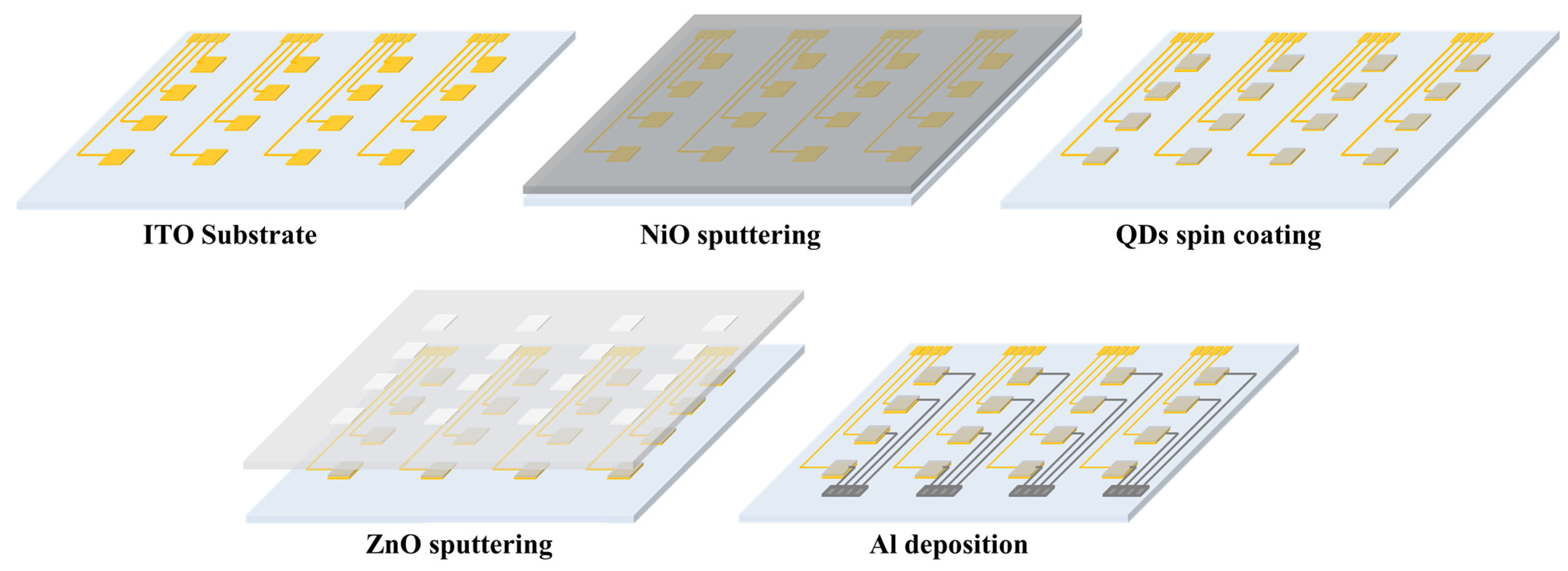
2.3. Device Fabrication
2.4. Device Measurement System
3. Results
3.1. Characteristics of the Synthesized PbS QDs
3.2. Performance of the SWIR Photodetector
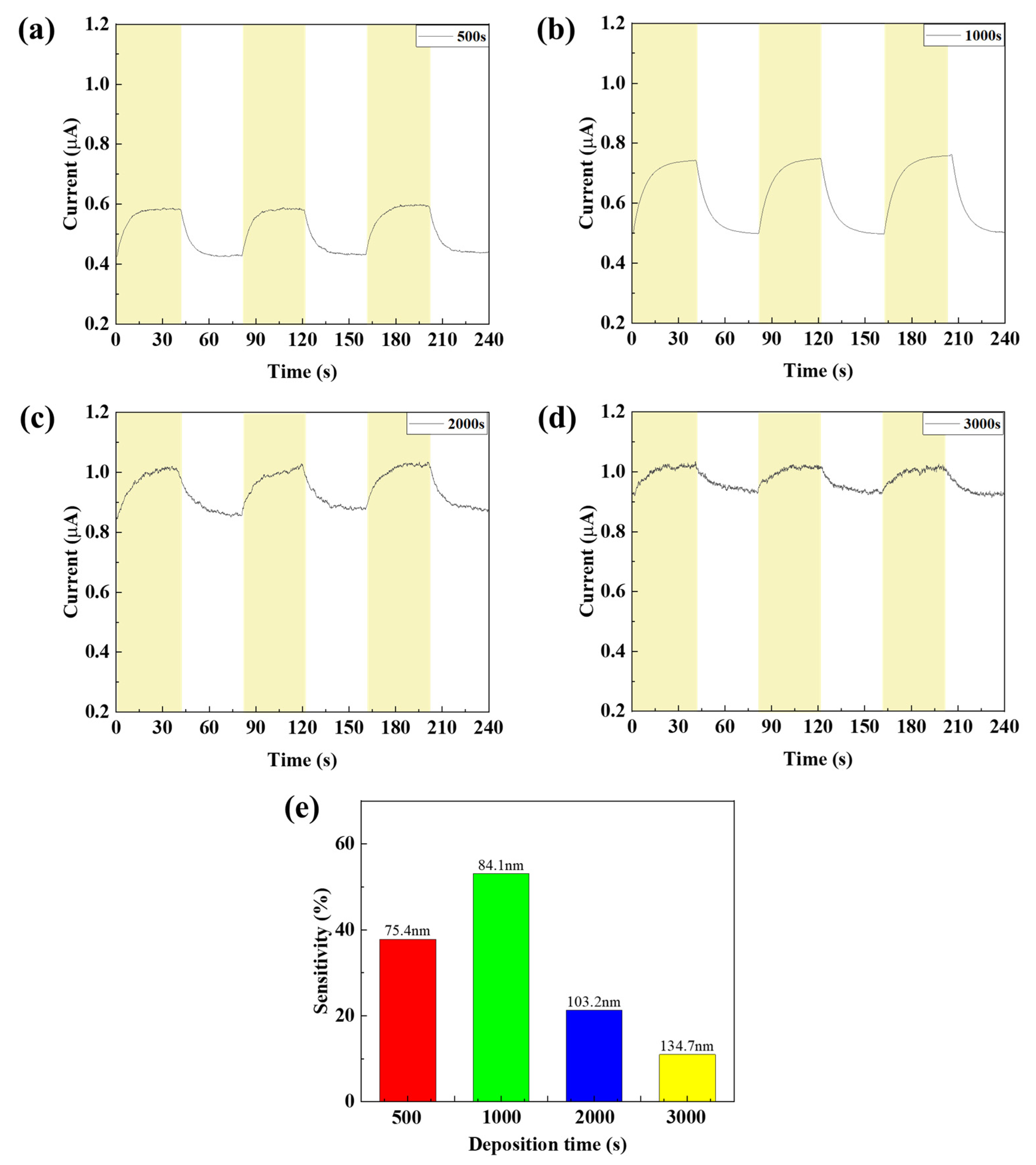
3.2.1. Characteristics According to ZnO Thin Film Thickness
3.2.2. Characteristics According to NiO Thin Film Thickness
3.2.3. Characteristics According to NiO Thin Film Annealing Conditions
4. Conclusions
Author Contributions
Funding
Data Availability Statement
Acknowledgments
Conflicts of Interest
References
- Arquer, F.P.; Armin, A.; Meredith, P.; Sargent, E.H. Solution-processed semiconductors for next-generation photodetectors. Nat. Rev. Mater. 2017, 2, 16100–16115. [Google Scholar] [CrossRef]
- Konstantatos, G.; Howard, I.; Fischer, A.; Hoogland, S.; Clifford, J.; Klem, E.; Levina, L.; Sargent, E.H. Ultrasensitive solution-cast quantum dot photodetectors. Nature 2006, 442, 180–183. [Google Scholar] [CrossRef] [PubMed]
- Michel, E.; Xu, J.; Kim, J.; Ferguson, I.; Razeghi, M. InSb infrared photodetectors on Si substrates grown by molecular beam epitaxy. IEEE Photonics Technol. Lett. 1996, 8, 673–675. [Google Scholar] [CrossRef]
- Graf, M.; Scalari, G.; Hofstetter, D.; Faist, J.; Beere, H.; Linfield, E.; Ritchie, D.; Davies, G. Terahertz range quantum well infrared photodetector. Appl. Phys. Lett. 2004, 84, 475–477. [Google Scholar] [CrossRef]
- Wu, W.; Bonakdar, A.; Mohseni, H. Plasmonic enhanced quantum well infrared photodetector with high detectivity. Appl. Phys. Lett. 2010, 96, 161107–161116. [Google Scholar] [CrossRef]
- Liu, H.C.; Li, J.; Thompson, J.; Wasilewski, Z.; Buchanan, M.; Simmons, J. Multicolor voltage-tunable quantum-well infrared photodetector. IEEE Electron Device Lett. 1993, 14, 566–568. [Google Scholar] [CrossRef]
- Gunapala, S.D.; Levine, B.F.; Ritter, D.; Hamm, R.; Panish, M.B. InGaAs/InP long wavelength quantum well infrared photodetectors. Appl. Phys. Lett. 1991, 58, 2024–2026. [Google Scholar] [CrossRef]
- Rauch, T.; Böberl, M.; Tedde, S.F.; Fürst, J.; Kovalenko, M.V.; Hesser, G.; Lemmer, U.; Heiss, W.; Hayden, O. Near-infrared imaging with quantum-dot sensitized organic photodiodes. Nat. Photon. 2009, 3, 332–336. [Google Scholar] [CrossRef]
- Takano, Y.; Masuda, M.; Kobayashi, K.; Kuwahara, K.; Fuke, S.; Shirakata, S. Epitaxial growth of InGaAs on misoriented GaAs (100) substrate by metal organic vapor phase epitaxy. J. Cryst. Growth 2002, 236, 31–36. [Google Scholar] [CrossRef]
- Hyder, S.B. Vapor-phase epitaxial growth of InGaAs lattice matched to (100) InP for photodiode application. Appl. Phys. Lett. 1979, 35, 787–789. [Google Scholar] [CrossRef]
- Lee, J.W.; Kim, D.Y.; Baek, S.; Yu, H.; So, F. Inorganic UV-Visible-SWIR broadband photodetector based on monodisperse PbS nanocrystals. Small 2016, 12, 1328–1333. [Google Scholar] [CrossRef] [PubMed]
- Hines, M.; AMbala, M.; Aigbavboa, C.; Aliu, J. Colloidal PbS nanocrystals with size-tunable near-infrared emission: Observation of post-synthesis self-narrowing of the particle size distribution. Adv. Mater. 2003, 15, 1844–1849. [Google Scholar] [CrossRef]
- Fu, H.Y.; Tsang, S.-W.; Zhang, Y.; Ouyang, J.; Lu, J.; Yu, K.; Tao, Y. Impact of the growth conditions of colloidal PbS nanocrystals on photovoltaic device performance. Chem. Mater. 2011, 23, 1805–1810. [Google Scholar] [CrossRef]
- Kwon, J.B.; Kim, S.-W.; Kang, B.-H.; Yeom, S.-H.; Lee, W.-H.; Kwon, D.-H.; Lee, J.-S.; Kang, S.-W. Air-stable and ultrasensitive solution-cast SWIR photodetectors utilizing modified core/shell colloidal quantum dots. Nano Converg. 2020, 7, 28. [Google Scholar] [CrossRef] [PubMed]
- Kwon, J.B.; Ha, Y.; Choi, S.; Jung, D.G.; An, H.K.; Kong, S.H.; Jung, D. Solution-processed NO2 gas sensor based on poly(3-hexylthiophene)-doped PbS quantum dots operable at room temperature. Sci. Rep. 2024, 14, 20600–20612. [Google Scholar] [CrossRef] [PubMed]
- McDonald, S.A.; Cyr, P.W.; Levina, L.; Sargent, E.H. Photoconductivity from PbS-nanocrystal/semiconducting polymer composites for solution-processible, quantum-size tunable infrared photodetectors. Appl. Phys. Lett. 2004, 85, 2089–2091. [Google Scholar] [CrossRef]
- Sulaman, M.; Yang, S.; Song, T.; Wang, H.; Wang, Y.; He, B.; Dong, M.; Tang, Y.; Song, Y.; Zou, B. High performance solution-processed infrared photodiode based on ternary PbSxSe1−x colloidal quantum dots. RSC Adv. 2016, 6, 87730–87737. [Google Scholar] [CrossRef]
- Heves, E.; Gurbuz, Y. PbS colloidal quantum dot photodiodes for SWIR detection. Procedia Eng. 2012, 47, 1426–1429. [Google Scholar] [CrossRef]
- Hechster, E.; Amgar, D.; Arad-Vosk, N.; Binyamin, T.; Sa’aR, A.; Etgar, L.; Sarusi, G. Electrical and optical characterization of quantum dots PbS/TiO2 based heterojunction as a SWIR detector and a proposed design of PbS/TiO2 PeLED as a SWIR to visible upconversion device. Mater. Res. Express 2019, 6, 066210–066218. [Google Scholar] [CrossRef]
- Oh, S.J.; Straus, D.B.; Zhao, T.; Choi, J.-H.; Lee, S.-W.; Gaulding, E.A.; Murray, C.B.; Kagan, C.R. Engineering the surface chemistry of lead chalcogenide nanocrystal solids to enhance carrier mobility and lifetime in optoelectronic devices. Chem. Commun. 2017, 53, 728–731. [Google Scholar] [CrossRef] [PubMed]
- Kwon, J.B.; Kim, S.; Lee, J.; Park, C.; Kim, O.; Xu, B.; Bae, J.; Kang, S. Uncooled short-wave infrared sensor based on PbS quantum dots using ZnO NPs. Nanomaterials 2019, 9, 926. [Google Scholar] [CrossRef] [PubMed]
- Zhao, H.; Chaker, M.; Wu, N.; Ma, D. Towards controlled synthesis and better understanding of highly luminescent PbS/CdS core/shell quantum dots. J. Mater. Chem. 2011, 21, 8898–8904. [Google Scholar] [CrossRef]
- Veeresh, K.; Sharma, H.; Singh, S.K.; Kumar, S.; Vij, A. Enhanced near-band edge emission in pulsed laser deposited ZnO/c-sapphire nanocrystalline thin films. Appl. Phys. A 2019, 125, 212–218. [Google Scholar]
- Kumar, R.; Kumar, M. Thickness effect of nanostructured ZnO thin films prepared by spray method on structural, morphological and optical properties. Microelectron. Eng. 2016, 151, 19–23. [Google Scholar] [CrossRef]
- Billaha, M.A.; Das, M.K. Performance analysis of AlGaAs/GaAs/InGaAs-based asymmetric long-wavelength QWIP. Appl. Phys. A 2019, 125, 457. [Google Scholar] [CrossRef]
- Cellek, O.O.; Ozer, S.; Besikci, C. High responsivity InP-InGaAs quantum-well infrared photodetectors: Characteristics and focal plane array performance. IEEE J. Quantum Electron. 2005, 41, 980–985. [Google Scholar] [CrossRef]
- Ghosh, S.; Bhattacharyya, A.; Sen, G.; Mukhopadhyay, B. Optimization of different structural parameters of GeSn/SiGeSn Quantum Well Infrared Photodetectors (QWIPs) for low dark current and high responsivity. J. Comput. Electron. 2021, 20, 1224–1233. [Google Scholar] [CrossRef]
- Ghosh, S.; Mukhopadhyay, B.; Sen, G.; Basu, P.K. Performance analysis of GeSn/SiGeSn quantum well infrared photo-detector in terahertz wavelength region. Phys. E Low-Dimens. Syst. Nanostructures 2020, 115, 113692. [Google Scholar] [CrossRef]
- Guériaux, V.; Nedelcu, A.; Coulibaly, A.; Marcadet, X.; March, K.; Enouz-Vedrenne, S. Structural and chemical study of AlGaAs/InGaAs based QWIPs. Infrared Phys. Technol. 2011, 54, 199–203. [Google Scholar] [CrossRef]
- Mahmodi, H.; Hashim, M.R.; Allahyarzadeh, G. Design and Study of a GeSn-SiGeSn Single Quantum Well Structure for Infrared Photodetection. In Proceedings of the 2012 International Conference on Enabling Science and Nanotechnology, Johor Bahru, Malaysia, 5–7 January 2012; pp. 1–2. [Google Scholar]
- Rodriguez, E.; Mottaghizadeh, A.; Gacemi, D.; Palaferri, D.; Asghari, Z.; Jeannin, M.; Vasanelli, A.; Bigioli, A.; Todorov, Y.; Beck, M.; et al. Room-temperature, wide-band, quantum well infrared photodetector for microwave optical links at 4.9 μm wavelength. ACS Photonics 2018, 5, 3689–3694. [Google Scholar] [CrossRef]
- Kim, M.; Han, C.-Y.; Yang, H.; Park, B. Band to band tunneling at the zinc oxide (ZnO) and lead selenide (PbSe) quantum dot contact; interfacial charge transfer at a ZnO/PbSe/ZnO probe device. Materials 2019, 12, 2289. [Google Scholar] [CrossRef] [PubMed]
- Nam, S.; Seo, J.; Woo, S.; Kim, W.H.; Kim, H.; Bradley, D.D.C.; Kim, Y. Inverted polymer fullerene solar cells exceeding 10% efficiency with poly(2-ethyl-2-oxazoline) nanodots on electron-collecting buffer layers. Nat. Commun. 2015, 6, 8929. [Google Scholar] [CrossRef] [PubMed]
- Hammad, A.H.; Abdel-wahab, M.S.; Vattamkandathil, S.; Ansari, A.R. Growth and Correlation of the Physical and Structural Properties of Hexagonal Nanocrystalline Nickel Oxide Thin Films with Film Thickness. Coatings 2019, 9, 615. [Google Scholar] [CrossRef]
- Gavale, H.S.; Wagh, S.; Ahirrao, R.B. Study of Physical Properties of Nanocrystalline NiO Thin Films Prepared by Spray Pyrolysis Technique. J. Nanosci. Technol. 2019, 5, 3. [Google Scholar] [CrossRef]
- Hossain, M.K.; Uddin, M.J.; Hossain, M.M. Effect of annealing temperature on the physical properties of NiO thin films and ITO/NiO/Al Schottky diodes. J. Mater. Sci. Mater. Electron. 2022, 33, 21060–21074. [Google Scholar]
- Sathyan, A.; Koppole, K. Thermal Annealing Effect on Properties of Nickel Oxide (NiO) Thin Films for Photovoltaic Applications. Phys. Status Solidi A 2025, 222, 2400784. [Google Scholar] [CrossRef]
- Xiao, X.; Xu, K.; Yin, M.; Qiu, Y.; Zhou, W.; Zheng, L.; Cheng, X.; Yu, Y.; Ning, Z. High quality silicon: Colloidal quantum dot heterojunction based infrared photodetector. Appl. Phys. Lett. 2020, 116, 101102. [Google Scholar] [CrossRef]
- Shikoh, A.S.; Choi, G.S.; Hong, S.; Jeong, K.S.; Kim, J. High-sensitivity hybrid PbSe/ITZO thin film-based phototransistor detecting from 2100 to 2500 nm near-infrared illumination. Nanotechnology 2022, 33, 165501. [Google Scholar] [CrossRef] [PubMed]
- Leemans, J.; Pejović, V.; Georgitzikis, E.; Minjauw, M.; Siddik, A.B.; Deng, Y.-H.; Kuang, Y.; Roelkens, G.; Detavernier, C.; Lieberman, I.; et al. Colloidal III–V quantum dot photodiodes for short-wave infrared photodetection. Adv. Sci. 2022, 9, 2200844. [Google Scholar] [CrossRef] [PubMed]
- Yang, J.; Lv, Y.; He, Z.; Wang, B.; Chen, S.; Xiao, F.; Hu, H.; Yu, H.; Liu, H.; Lan, X.; et al. Bi2S3 electron transport layer incorporation for high-performance heterostructure HgTe colloidal quantum dot infrared photodetectors. ACS Photonics 2023, 10, 2226–2233. [Google Scholar] [CrossRef]
- He, Z.; Liu, H.; Xie, F.; Bai, M.; Wen, S.; Zhao, J.; Liu, W.; Liao, M. Lead Selenium Colloidal Quantum Dots for 400–2600 nm Broadband Photodetectors. J. Nanomater. 2022, 2022, 1–8. [Google Scholar] [CrossRef]
- Wang, X.; Xu, K.; Yan, X.; Xiao, X.; Aruta, C.; Foglietti, V.; Ning, Z.; Yang, N. Amorphous ZnO/PbS quantum dots heterojunction for efficient responsivity broadband photodetectors. ACS Appl. Mater. Interfaces 2020, 12, 8403–8410. [Google Scholar] [CrossRef] [PubMed]
- Dias, S.; Kumawat, K.; Biswas, S.; Krupanidhi, S.B. Solvothermal synthesis of Cu2SnS3 quantum dots and their application in near-infrared photodetectors. Inorg. Chem. 2017, 56, 2198–2203. [Google Scholar] [CrossRef] [PubMed]
- Wang, Y.; Peng, L.; Schreier, J.; Bi, Y.; Black, A.; Malla, A.; Goossens, S.; Konstantatos, G. Silver telluride colloidal quantum dot infrared photodetectors and image sensors. Nat. Photonics 2024, 18, 236–242. [Google Scholar] [CrossRef]


| Deposition Time (s) | Thickness (nm) | Band Gap (eV) |
|---|---|---|
| 500 | 75.4 | 3.45 |
| 1000 | 84.1 | 3.39 |
| 2000 | 103.2 | 3.28 |
| 3000 | 134.7 | 3.18 |
| Deposition Time (s) | Thickness (nm) | Transmittance (%) | Grain Size (nm) |
|---|---|---|---|
| 2000 | 91 | 64.3 | 34.114 |
| 3000 | 161 | 66.1 | 38.581 |
| 4000 | 216 | 67.3 | 40.745 |
| 5000 | 274 | 64 | 44.38 |
| Temperature (°C) | Transmittance (%) | Grain Size (nm) |
|---|---|---|
| R.T. | 71.3 | 40.745 |
| 150 | 74.1 | 44.872 |
| 300 | 75.8 | 47.937 |
| 400 | 73.6 | 49.264 |
| Temperature (°C) | Transmittance (%) | Grain Size (nm) |
|---|---|---|
| R.T. | 71.3 | 40.745 |
| 1 | 74.1 | 44.872 |
| 2 | 74.5 | 45.127 |
| 3 | 75.0 | 49.724 |
| 4 | 75.4 | 51.548 |
| Material | Device Structure | Response Band (nm) | Responsivity (A/W) | Ref. |
|---|---|---|---|---|
| PbS | Si/ZnO/PbS | 1310 | 0.22 | [38] |
| PbSe | InSnZnO/PbSe | 2100 | 3.91 × 10⁻³ | [39] |
| In(As,P) | ITO/NiO/In(As,P)/TiO2/Al | 1400 | 7 × 10⁻³ | [40] |
| HgTe | Bi2S3/HgTe/Ag:HgTe | 2200 | 0.29 | [41] |
| PbSe | PbSe | 400−2600 | 0.32 | [42] |
| PbS | ZnO/PbS | 1310 | 0.47 | [43] |
| Cu2SnS3 | ITO/Cu2SnS3/Ag | 1550 | 0.9 × 10⁻³ | [44] |
| Ag2Te | Ag2Te/AgNiS2/SnO2 | 350−1600 | 0.1 | [45] |
| PbS | ITO/NiO/PbS/ZnO/Al | 1405 | 0.23 | This work |
Disclaimer/Publisher’s Note: The statements, opinions and data contained in all publications are solely those of the individual author(s) and contributor(s) and not of MDPI and/or the editor(s). MDPI and/or the editor(s) disclaim responsibility for any injury to people or property resulting from any ideas, methods, instructions or products referred to in the content. |
© 2025 by the authors. Licensee MDPI, Basel, Switzerland. This article is an open access article distributed under the terms and conditions of the Creative Commons Attribution (CC BY) license (https://creativecommons.org/licenses/by/4.0/).
Share and Cite
Kwon, J.; Ha, Y.; Choi, S.; Jung, D. Development of a Highly Reliable PbS QDs-Based SWIR Photodetector Based on Metal Oxide Electron/Hole Extraction Layer Formation Conditions. Nanomaterials 2025, 15, 1107. https://doi.org/10.3390/nano15141107
Kwon J, Ha Y, Choi S, Jung D. Development of a Highly Reliable PbS QDs-Based SWIR Photodetector Based on Metal Oxide Electron/Hole Extraction Layer Formation Conditions. Nanomaterials. 2025; 15(14):1107. https://doi.org/10.3390/nano15141107
Chicago/Turabian StyleKwon, JinBeom, Yuntae Ha, Suji Choi, and Donggeon Jung. 2025. "Development of a Highly Reliable PbS QDs-Based SWIR Photodetector Based on Metal Oxide Electron/Hole Extraction Layer Formation Conditions" Nanomaterials 15, no. 14: 1107. https://doi.org/10.3390/nano15141107
APA StyleKwon, J., Ha, Y., Choi, S., & Jung, D. (2025). Development of a Highly Reliable PbS QDs-Based SWIR Photodetector Based on Metal Oxide Electron/Hole Extraction Layer Formation Conditions. Nanomaterials, 15(14), 1107. https://doi.org/10.3390/nano15141107