Article

First-Principles Study of Halide Modulation on Deep-Level Traps in FAPbI3

1
National Laboratory of Solid State Microstructures, Department of Physics, Nanjing University, Nanjing 210093, China
2
Institute of Materials Engineering, Nantong 226019, China
*
Author to whom correspondence should be addressed.
Nanomaterials 2025, 15(13), 981; https://doi.org/10.3390/nano15130981
Submission received: 11 May 2025 / Revised: 12 June 2025 / Accepted: 22 June 2025 / Published: 24 June 2025

Abstract

In this study, we investigate the influence of the halogen elements bromine (Br) and chlorine (Cl) on iodine defect properties primarily in FAPbI3 through first-principles calculations, aiming to understand the effect of high defect densities on the efficiency of organic–inorganic hybrid perovskite cells. The results indicate that Br and Cl interstitials minimally alter the overall band structure of FAPbI3 but significantly modify the defect energy levels. Br and Cl interstitials, with defect states closer to the valence band and lower formation energies, effectively convert deep-level traps induced by iodine interstitials (Ii) into shallow-level traps. This conversion enhances carrier transport by reducing non-radiative recombination while preserving light absorption efficiency. Excess Br/Cl co-doping in FAPbI3 synthesis thereby suppresses non-radiative recombination and mitigates the detrimental effects of iodide-related defects.

1. Introduction

In recent years, solar cells based on halide perovskites, such as XPbI3 (X = Cs, CH3NH3, NH2CHNH2, etc.) have received widespread attention because of their advantages such as adjustable bandgap, high light absorption rate, low carrier recombination rate, and high photoelectric conversion efficiency (PCE) [1,2,3], which facilitate efficient charge collection and achieve higher PCE [4]. Due to these favorable optoelectronic properties, the PCE of single-junction perovskite solar cells (PSCs) has surged remarkably from 3.8% to over 26% within the past decade [5,6,7]. Among them, MAPbI3 (CH3NH3PbI3) and FAPbI3 (NH2CHNH2PbI3) have been the most studied. Compared with MAPbI3, FAPbI3 has a more symmetrical crystal structure and a more optimum theoretical bandgap of 1.48 eV [8], approaching the Shockley–Queisser limit for single-junction cells (approximately 33.7%) [5,6,9]. Moreover, FAPbI3 has better thermal stability and is not easily degraded [7]. Although the photoactive phase of FAPbI3 is unstable at operating temperatures and tends to transform into the photoinactive yellow phase [8], it remains a highly promising optoelectronic material because stabilization is achievable through doping with Zn (II) cations and formate anions, along with other strategies [10].
Despite rapid efficiency improvements, FAPbI3 faces a significant challenge in high intrinsic defect density. The soft lattice of synthesized halide perovskite solutions and films [5], combined with tilted FA cations within the relaxed PbI6 framework [11,12], induces strong lattice distortion that inevitably generates high defect concentrations [13,14,15]. While shallow defects dominate in halide perovskites [16], recent studies confirm the coexistence of detrimental deep-level traps in FAPbI3 [12,16,17,18]. The deep energy levels inside the bandgap usually have high ionization energy [19] and act as potent non-radiative recombination centers. By capturing charge carriers, they reduce carrier lifetimes, degrade open-circuit voltage (Voc), and ultimately limit device performance [20,21]. Consequently, even with advanced crystal growth techniques, FAPbI3 polycrystalline films exhibit high defect densities (9.6 × 10¹⁵~1.37 × 1016 cm−3) [22], exceeding those in classical semiconductors (typically 108–1015 cm−3) [23,24,25,26] by orders of magnitude. This severely suppresses device efficiency. Although FAPbI3 exhibits some defect tolerance [27,28], strategies to mitigate defects remain crucial for further performance gains. The high defect density issue can currently be addressed through light soaking, chemical passivation, interface engineering, and microstructure modulation methods [29]. Recent studies demonstrate that doping and passivation with homologous halide ions effectively enhances halide perovskite performance. Mu et al. [30] found that 20% chlorine doping increases FAPbI3 power conversion efficiency. Energy-dispersive X-ray analysis confirms that the film’s chlorine contents match the precursor solution ratio, indicating precise chlorine doping improves FAPbI3 properties. Multi-halide co-doping shows significant performance optimization effects. Mariotti et al. [31] achieved 1.28 eV open-circuit voltage in single-junction cells and 32.5% certified tandem efficiency using triple-halide (I, Br, and Cl) perovskite with piperazine iodide interface engineering for perovskite–silicon tandem solar cells. Xu et al. [32] resolved phase separation through trihalide incorporation and established Br-mediated I-Cl lattice connections, realizing bulk chlorine doping that doubled carrier mobility and lifetime.
Current understanding remains limited regarding defect property modulation in halide perovskites through halide doping, and quantitative analyses of carrier transport and recombination effects are necessary. This study employs first-principles calculations to investigate intrinsic point defects in FAPbI3 and interstitial defect properties of bromine, chlorine, and fluorine. The calculations include defect formation energies, transition levels, and migration. The results show bromine and chlorine interstitial defects exert less influence on FAPbI3 performance than intrinsic iodine interstitials, accompanied by decreased migration rates. These defect property changes provide insights into FAPbI3 performance enhancement via halide doping.

2. Calculation Methods

This paper employs the Vienna ab initio Simulation Package (VASP 5. 3. 5), a computational software based on density functional theory [33]. The initial structure of FAPbI3 was constructed using experimentally reported perovskite geometries [34,35]. In examining the defect formation energy (DFE) of point defects in FAPbI3, a 2 × 2 × 2 supercell is employed (as shown in Figure S1), with a point defect formed into the supercell to facilitate the averaging of defect volume [36]. A plane–wave energy cutoff of 500 eV and a 5 × 5 × 5 k-point grid using the Monkhorst–Pack method were employed in the calculations. Structural relaxations were conducted until forces on atoms fell below 0.01 eV/Å, and energy convergence reached 1 × 10⁻⁶ eV. To account for van der Waals interactions, the rev-vdW-DF2 functional proposed by Hamada [37] was employed, ensuring full optimization of atomic positions and lattice parameters.
The effect of spin–orbit coupling (SOC) has been previously reported in Pb-based perovskites, but the predicted bandgap is significantly lower than the experimental value [38]. To obtain accurate bandgap values for qualitative analysis, we employed the G0W0 method with spin–orbit coupling (SOC) effects included [39,40], and the calculated bandgap is 1.50 eV, consistent with experimental values [41]. For the calculation of charged defects, it is assumed that the additional or missing electrons from charged defects come from an external electron reservoir or enter the supercell interior with their energy equivalent to the Fermi energy, using Equation (1) [42]:
DFE = E ( defect ) E ( prefect ) + i n i μ i + q ( E F + E V B M ) + E c o r r
where E ( defect ) represents the system containing defects, E ( prefect ) is the energy of the perfect system without defects, and n and μ are the number of atoms and the corresponding chemical potentials individually. For vacancy defects, ni > 0, and interstitial defects, ni < 0. In order to ensure the formation of perovskite, the chemical potentials of FA, Pb, and I satisfy the following relationship:
μ F A + μ P b + 3 μ I = Δ H FAPbI 3
Here, Δ H represents the formation energy of perovskite in the cubic phase. We selected the cubic phase of Pb solid, the orthorhombic phase of I2 solid, and the cubic phase of FA to calculate their chemical potentials, respectively. In order to prevent the formation of FAI and PbI2 as by-products, it is necessary to ensure that the chemical potential values satisfy the following conditions:
μ F A + μ I < Δ H ( FAI )
μ P b + 2 μ I < Δ H ( PbI 2 )
In accordance with Equations (2)–(4), the chemical potential regions under equilibrium growth conditions for the perovskite were calculated. In this research, the moderate chemical potentials of FA, Pb, and I were selected for calculating DFE (details of the chemical potential calculations are provided in Figure S2 and Table S1). In the last term q ( E F + E V B M ) + Δ V , q represents the charge of the defect; EVBM represents the energy level at the top of the valence band, and EF is the Fermi level at the top of its relative valence band. At the top of the valence band E F = 0 , the Fermi levels are permitted to fluctuate within the bandgap, with the upper limit of the valence band maximum (VBM) aligning with the lower limit of the conduction band minimum (CBM) in a defect-free FAPbI3 crystal, which serves as the reference point for the bandgap. E c o r r is a correction term added to avoid spurious interactions of charged defects between supercells so that the potential energy in the defective supercells corresponds to the bulk potential energy (as shown in Supporting Information) [43,44]. Equation (1) shows that the formation energy of charged defects depends linearly on the Fermi level within the bandgap, with the slope determined by the charge state q. Consequently, defects of the same type can exhibit different formation energies for different charge states. The intersection points of these formation energy lines define the defect transition levels ε ( q 1 / q 2 ) between charge states [36]. Additionally, distinct charge states may correspond to distinct local atomic configurations [45,46,47]. Defect transition levels determine electronic behavior and are often used as a basis for experimental detection or identification of defects. Therefore, accurate calculation of the defect transition level is essential for the identification and characterization of defects. The specific calculation can be expressed by the following formula:
ε ( q 1 / q 2 ) = D F E q 1 D F E q 2 q 2 q 1
where D F E q n is the DFE for a charge state of q n . Figure 1 illustrates Equation (5). When the Fermi level lies below (+/0), the q = +1 charge state remains stable. When the Fermi level exceeds (+/0), the q = 0 state becomes stable. The (+/0) position defines the defect transition level (trap level). Similar principles apply to (0/−). The trap level position relative to band edges determines whether defects act as deep-level or shallow-level centers. Deep-level defects form when trap levels reside within the bandgap (mid-gap). These deep centers degrade carrier mobility [48].

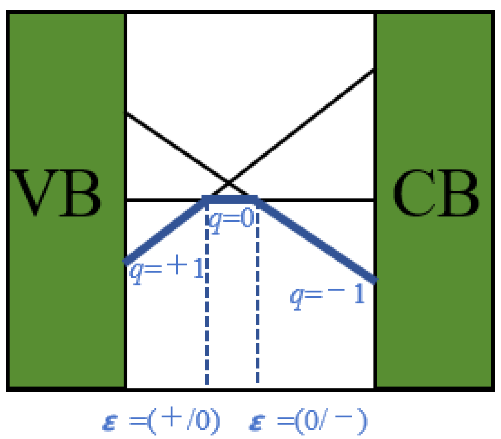
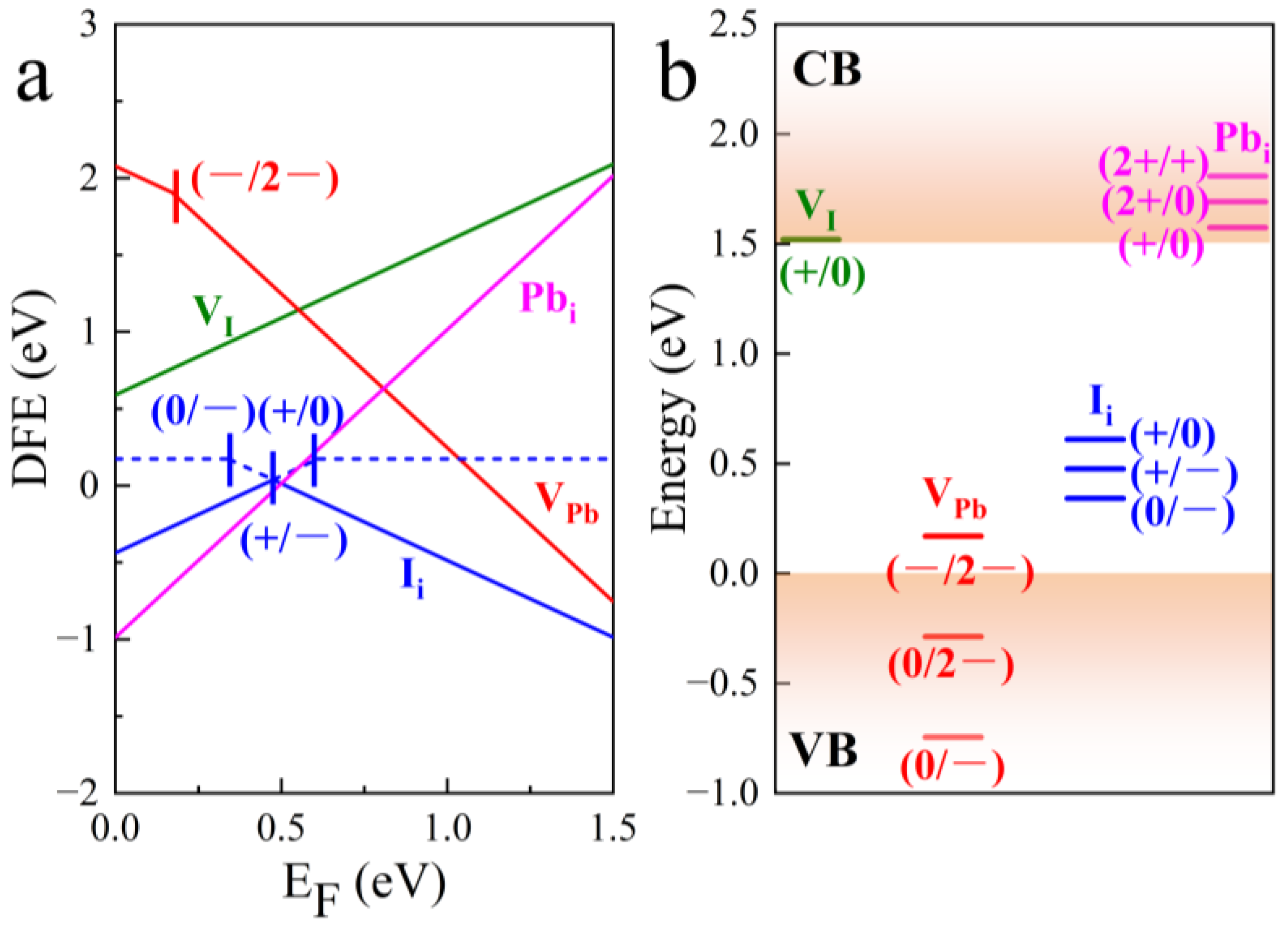
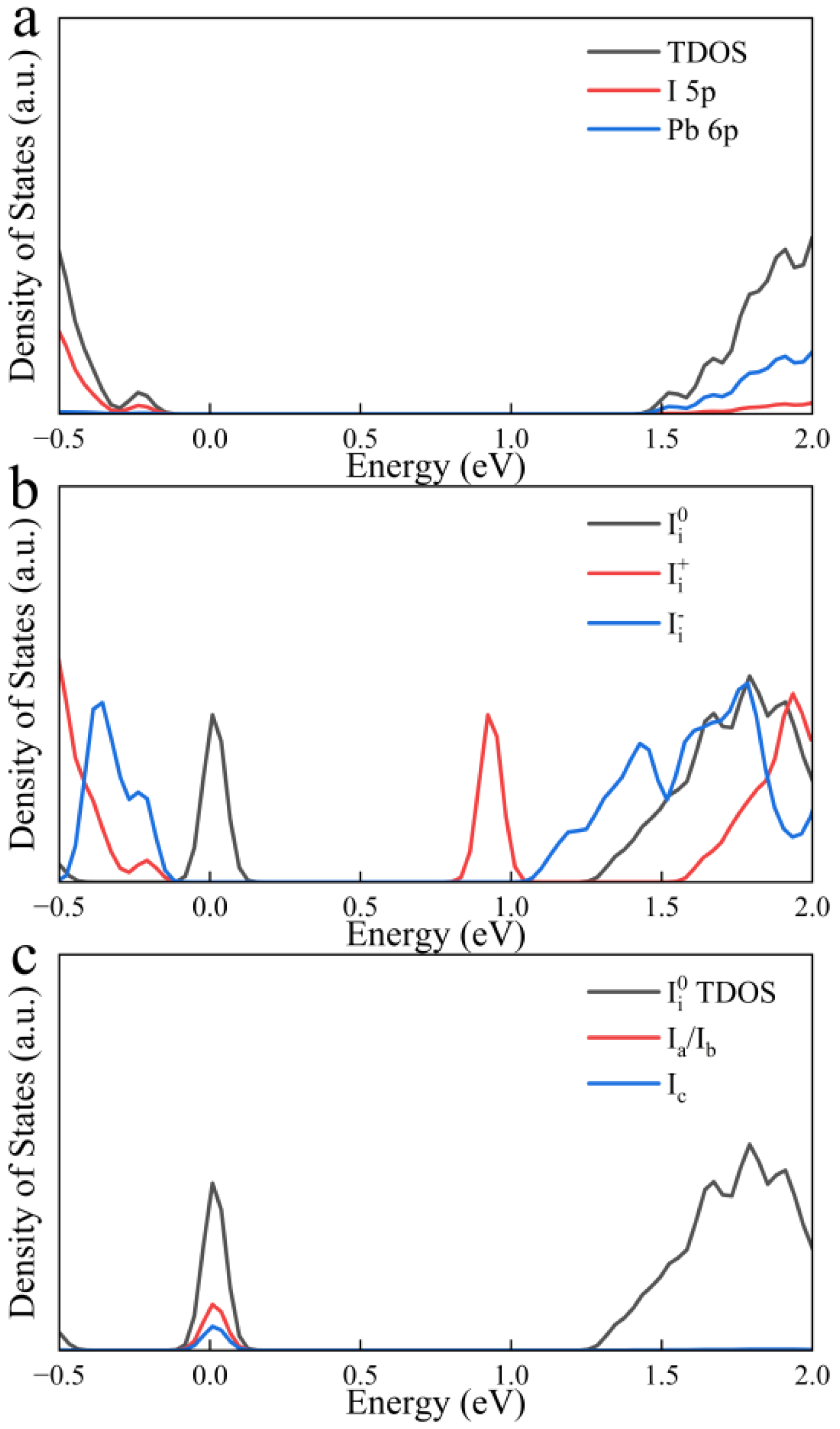
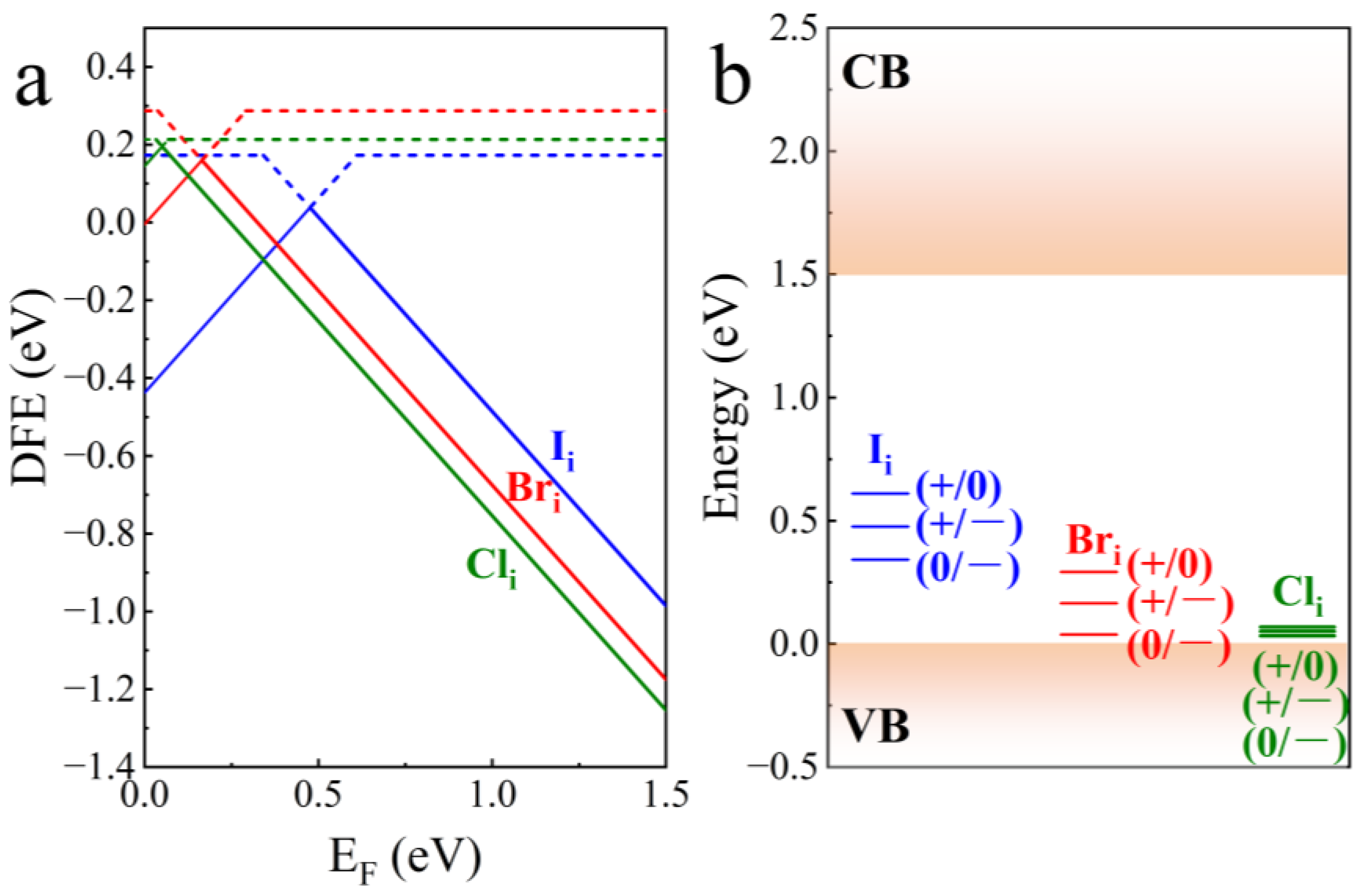
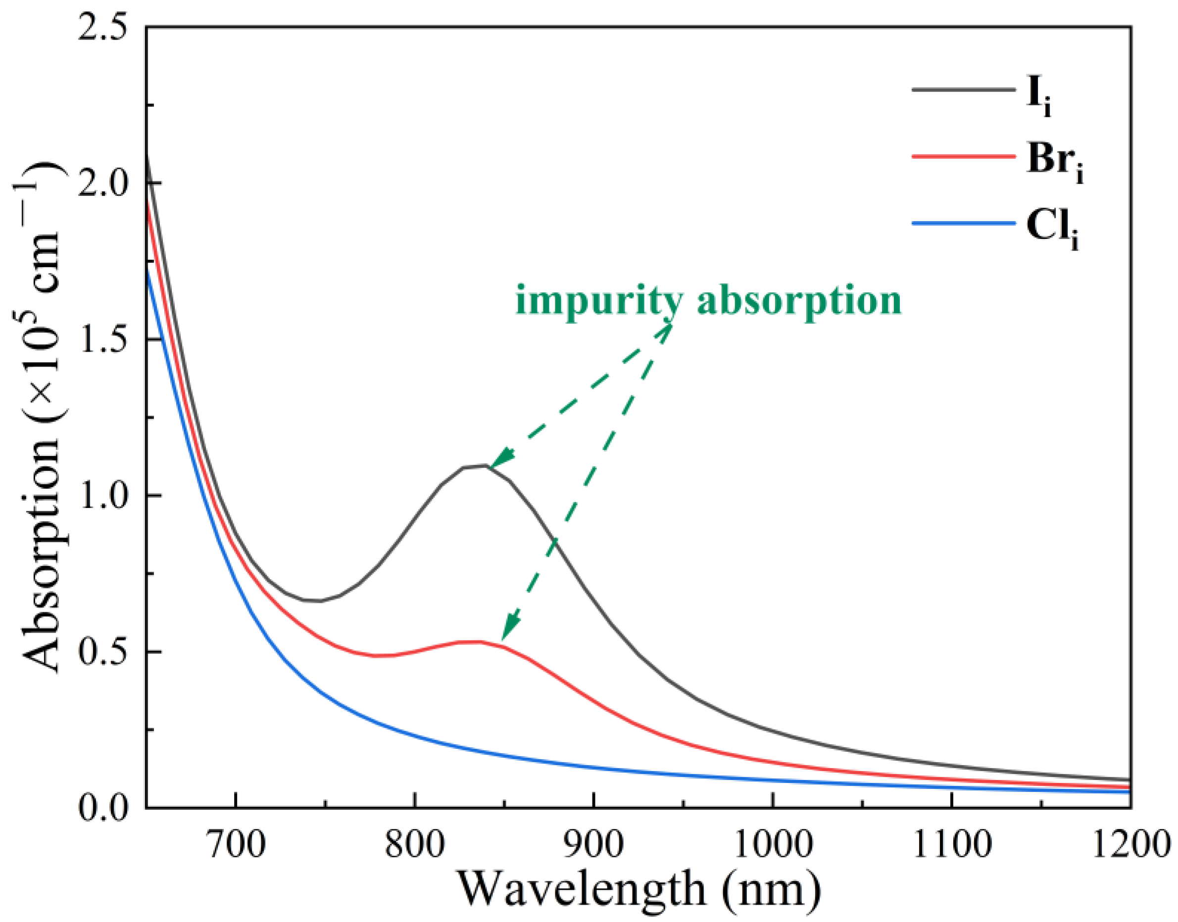
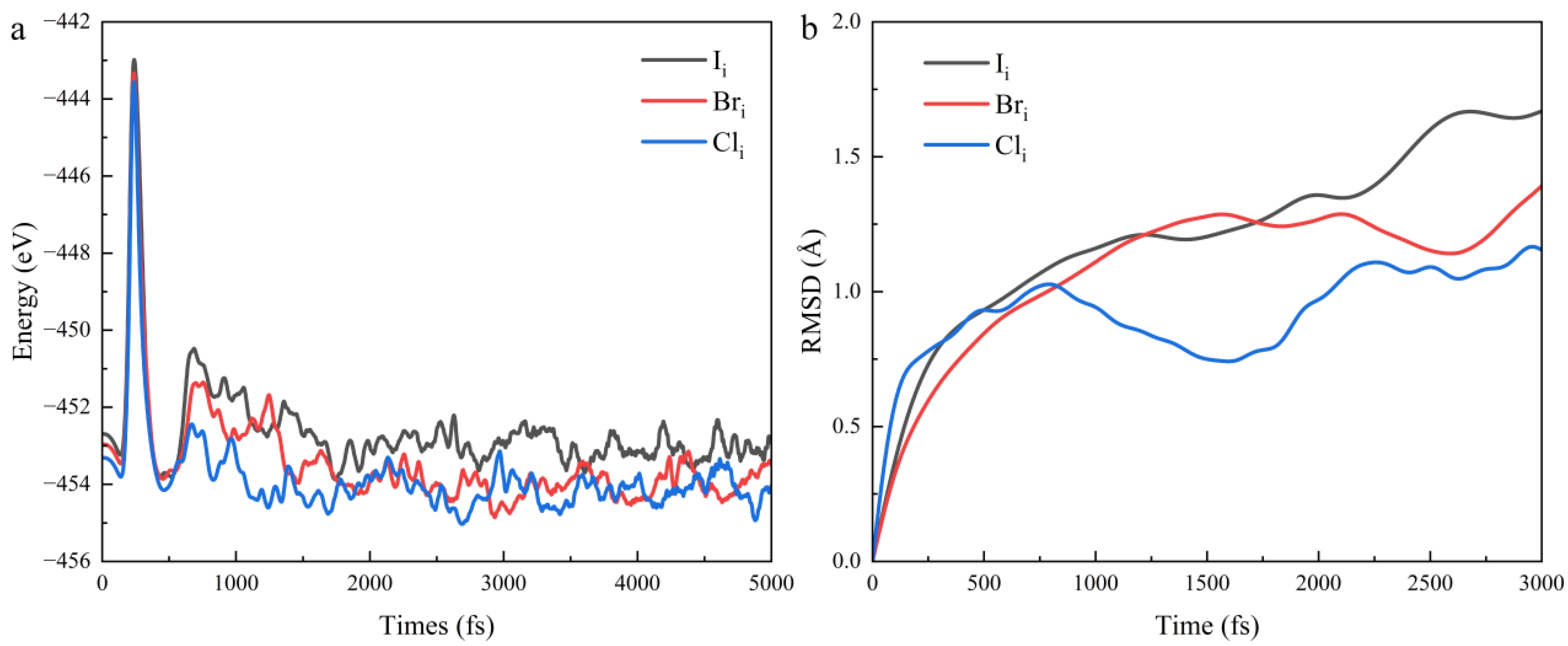
3. Results and Discussion

Because organic cations in perovskite make little or no contribution to the electronic states at the edges of the energy bands, here, we ignore the effect of point defects associated with FA cations [39]. The defect formation energies of an iodine vacancy (VI), iodine interstitial (Ii), lead vacancy (VPb), and lead interstitial (Pbi) have been calculated and are shown in Figure 2a. The lowest formation energy defects are Pbi and Ii, which represent the fact that Pbi and Ii are more likely to form and stabilize under thermodynamic equilibrium, implying a higher defect density. Stabilized Ii has a lower DFE. Figure 2a shows that Ii exists in neutral (0), negatively charged (−), and positively charged (+) states, with the stable charge state being the transition from + to −, forming a more stable negatively charged state. Similarly, Pbi is also a relatively stable type of defect, with the stable charge state being 2+. In addition to these stable defects, the stable charge state for VI within the bandgap is +, and for VPb, it is −/2−, with the charge state reaching the lowest DFE being 2−. From the thermodynamic level, point defects are more prone to forming interstitial defects with lower DFEs. This phenomenon may be attributed to the soft lattice characteristics of FAPbI3, which facilitate the easier occupation of interstitial positions within the lattice by adding additional atoms [5]. While all defects will influence the position of the Fermi level, their effect will diminish exponentially with increasing DFE. The more stable Ii defect, for instance, affects the intrinsic Fermi level of the perovskite. In addition to considering the number of defects, it is also important to take into account their activity. This refers to the migration rate of the defects, as thermodynamically favorable defects may be limited by high migration activation energies, which prevent their migration. It is commonly accepted that interstitial defects are more prone to migration than vacancy defects [47], and defects associated with iodine exhibit a higher migration rate than those linked to lead [49,50]; thus, it can be reasonably deduced that defects related to iodine ions may become the primary migration targets [51,52,53]. Furthermore, defect transition levels (trap levels) critically influence charge carrier dynamics and photovoltaic performance in perovskite materials. Although some defects exhibit low defect formation energy, their impact on carrier transport depends primarily on trap level positions within the bandgap [54]. These trap levels act as non-radiative recombination centers, while charged defects reduce conductivity through carrier scattering. Crucially, halide perovskites demonstrate good defect tolerance because defect-induced trap levels typically reside near band edges, minimizing disruption to carrier transport.
Figure 2a shows the defect formation energy (DFE); under thermodynamic equilibrium, the stable charge states for VPb within the bandgap are −/2−, indicating that the defect can further capture holes through the trap levels shown in Figure 2b, releasing energy, hence the lower DFE for the 2− charge state. Since the neutral charge state of VPb is not stable under thermodynamic equilibrium, and the 0/2− and 0/− charge state transition levels are within the valence band, no deep-level traps are formed, meaning that the neutral charge state defect of VPb can be neglected. Furthermore, the 2− charge state migration activation energy of VPb indicates that metallic lead is only likely to nucleate on the surface under high temperatures or under illumination [55], so the impact of VPb on FAPbI3 is not significant. Ii can capture electrons and holes through the +/0 and 0/− trap levels at 0.89 eV below the conduction band (CB) and 0.34 eV above the valence band (VB), respectively, acting as both a donor and an acceptor within the bandgap. The stable trap levels at the thermodynamic level, as illustrated in Figure 2a, are in close proximity to the Fermi level of FAPbI3. This indicates that the trap level exerts a considerable influence on the electronic states situated in proximity to the Fermi surface. Thus, FAPbI3 performance degrades significantly because all trap levels reside within the bandgap, and deep-level traps actively capture carriers, reducing carrier lifetime. As shown in Figure 2b, all trap levels of Pbi and VI are located inside the CB, and there are no trap levels inside the bandgap, which makes it difficult to form a recombination center and has less effect on the carrier transport. Moreover, the +/0 trap level of VI and Pbi show shallow trapping behavior at the bottom of the CB, with some polarization around the defect location, and have a resonance with the CB, so that despite the migration activation energy being low, it can still act as a shallow-level trap [56]. From the above conclusion, Ii defects can be considered as the most likely point defect to exist stably and trap carriers because they have the lowest DFE with deep-level traps.
To further investigate the effect of Ii on FAPbI3, we calculated the density of states in the case of Ii, and the density of states calculation from Figure 3a shows that the conduction band of FAPbI3 is mainly contributed by electrons in the 6p orbital of Pb atoms, while the valence band is mainly contributed by electrons in the 5p orbital of I atoms. Other elements introduce deep-level states within the VB and CB. These states do not participate in bonding and contribute negligibly to the density of states near the band edges.
As shown in Figure 3b, the different charge states of Ii form traps inside the bandgap with different energy level positions, I i 0 creates a new trap level within the bandgap that can trap either holes or electrons, but according to the Pauli exclusion principle, these two processes cannot occur at the same time, and since its location is closer to the VB, hole trapping can become a dominant process, and as more holes are trapped, the holes that accumulate in the trap level can trap a large number of photo-excited electrons in the valence band, making it more difficult for valence band electrons to transition to the conduction band, reducing the number of electrons that can be collected by the electron transport layer. It is worth noting that due to the close proximity of the trap level location to the VBM if the defect concentration is too high, Fermi level pinning will form, which further enhances non-radiative recombination of electrons and holes and reduces carrier concentration, which consequently decreases both open-circuit voltage and short-circuit current, and induces more pronounced hysteresis [57,58,59]. By observing the I i 0 DOS of Figure 3c, it is found that the interstitial I atom has the same peak position of state density with its neighboring I atoms b and c, indicating that I ions adjacent to this interstitial atom contribute to the formation of the defect state I i does not create new trap levels inside the bandgap. This phenomenon arises because the interstitial iodine anion forms an I-Pb bond with the lead ion, which eliminates the unsaturated suspension bond and moves the trap state into the VB, which helps to eliminate the effect of electron–phonon coupling on the lattice.
In the I i + system, the trap level formed by positively charged iodine cations is located below the CBM, and this trap state can act as an electron acceptor to capture the electrons of valence band transitions, forming electron traps and accelerating non-radiative recombination. In addition, the positively charged interstitial iodide cations are prone to form I trimers by mutual attraction with the point anions on the lattice, which leads to an increase in the number of trapping sites and will result in the localization of charge density to itself, thus reducing the charge density of the VBM and CBM.
The results from previous molecular dynamics simulations suggest that trap levels can be eliminated and carrier lifetimes extended by oxidizing I i 0 to I i [60]. However, I i is unstable under light conditions, and holes are easily captured and converted back to I i 0 again, reducing the performance of perovskite [48,61]. The preceding analysis indicates that the impact of Ii on the electronic structure of perovskite is more pronounced among the point defects.
In order to minimize the effect of Ii on FAPbI3, based on the same model, we investigated the possible effect of substitution of Ii by the halides Bri and Cli on FAPbI3. From the DFE of Figure 4a, it can be seen that the negative charge states (−) of Bri and Cli, which are stabilized inside the bandgap at the thermodynamic level, are the most stable, which is the same as that of Ii, and the magnitude of the DFE is Ii > Bri > Cli, which represents the fact that Bri and Cli are more likely to form, this may be due to the fact that Cl and Br with smaller ionic radii than I are more likely to form interstitial defects that do not cause excessive distortion stresses on the lattice leading to elastic distortions, and therefore require less energy cost and are more likely to occupy interstitial positions in the lattice, and these smaller ionic radii may be more likely to chemically bond with neighboring atoms or ions, resulting in stable chemical bonding with fewer dangling bond effects on the defect state [62]. Compared with Ii, the trap levels of Bri and Cli demonstrated in Figure 4b become more concentrated, the transition levels of defects between different charge states occur more easily with less energy change required, and the trap level as a whole is significantly more biased towards the valence band, gradually shifting from deep-level traps inside the bandgap to shallow-level traps, implying that electrons or holes captured by the trap state can be easily ionized by smaller ionization energies. This renders it difficult to form recombination centers, which reduces the impact on carrier transport, consistent with the improved photovoltaic performance reported in previous studies [63].
We also calculated defect formation energy for Fi replacing Ii, as shown in Figure S3a. The defect formation energy of Fi is significantly higher than that of Ii, Bri, and Cli. This indicates that Fi formation in FAPbI3 is energetically unfavorable, making it difficult for Fi to occupy Ii sites. Additionally, fluorine demonstrates inferior trap level modulation capability compared with bromine and iodine in Figure S3b. Fluorine ions likely exhibit minimal impact on regulating deep-level traps in FAPbI3. Subsequent discussions will focus on Bri and Cli properties.
Given the low formation energies of Bri and Cli and their lack of deep-level traps, we investigated their electronic density of states (DOS). Figure 5a reveals that substituting lattice iodine with bromine or chlorine introduces no in-gap states and only slightly widens the bandgap. This suggests minimal disruption to the fundamental electronic structure of FAPbI3 and largely preserved electronic transport properties. From Figure 5b, it can be found that at a charge state of 0, compared with I i 0 , Br i 0 , and Cl i 0 make the positions of VB and CB shifted upwards as a whole, which causes the positions of the trap levels to be progressively closer to the valence band, which is more susceptible to ionization. The trap levels formed by the positive charge defects in Figure 5c are located deep in the bandgap, and due to the +/− charge state transitions, there is a trapping behavior of electrons. The positively charged defects act as electron acceptors, and the trap level of I i + is close to CB; thus, it is expected that the trapping of the electrons will take place much more rapidly, whereas the trapping of electrons becomes more and more difficult in the case of Br i + and Cl i + because of the gradual location of trap levels closer to the VB, it is notable that the positively charged defects, Bri and Cli, are not the lowest energy of formation at the thermodynamic level. Consequently, the density of these defects is not expected to be particularly high.
The reduced formation energies of Bri and Cli suppress the generation of Ii defects. Compared with the deep-level traps formed by Ii, shallow-level traps exert less detrimental effects on carrier transport, which may benefit the performance of FAPbI3. This suggests that Br/Cl doping effectively inhibits non-radiative recombination and prolongs carrier lifetime in halide perovskites, consistent with recent experimental studies. For instance, Zhang et al. [64] used synchrotron-based XRD and XPS to demonstrate that Cl-terminated ligands optimize halogen distribution in FAPbBr3-xClx nanocrystalline films. This optimization induces a 9 nm blue shift in the PL peak and a 1.6-fold increase in exciton binding energy, confirming reduced deep-level traps. Similarly, Br-rich surfaces in CsPbBr3 nanosheets significantly enhance the PLQY (from 31.15% to 87.2%) and extend carrier lifetime (to 16.69 ns), as reported by Varnakavi et al. [65]. These improvements further evidence the defect-passivation effect of Br doping.
The aforementioned conclusions lead to the conclusion that Bri and Cli primarily influence defect properties rather than the fundamental electronic structure of FAPbI3. To further investigate their capacity to modulate Ii defects, we examined the impact of the defects on the nature of light absorption. Figure 6 illustrates the optical absorption coefficient versus wavelength for FAPbI3 with Ii, Bri, and Cli interstitial defects. These results demonstrate that the intrinsic absorption of FAPbI3 remains nearly identical regardless of Ii, Bri, or Cli interstitial defects, confirming consistent optical bandgaps. The absorption observed in long-wavelength regions originates from FAPbI3 containing Ii defects, indicating defect-mediated absorption.
The absorption edge that emerges after adding impurities to the absorption peak suggests that the defect is fully ionized. The impurity absorption position of Bri is slightly blue-shifted, and the absorption peak is diminished, which suggests that Bri trap level necessitates less ionization energy. Additionally, Cli exhibits negligible impurity absorption because of its shallow trap levels, consistent with its rapid ionization behavior., which corresponds to the previous Figure 5b, the shallow-level trap of Cli is readily ionized. The suppression of the trap level by Br and Cl has been demonstrated to effectively reduce the effect of I on the light-absorbing properties of FAPbI3, as evidenced by the absorption spectra.
To evaluate the dynamic behavior of different interstitial defects (Ii, Bri, and Cli), we performed molecular dynamics (MD) simulations at 300 K using the NVT ensemble with a Langevin thermostat [66,67]. The simulations utilized a time step of 1 fs and spanned 5 ps after equilibration. As shown in Figure 7a, the energy fluctuations of the three supercells are within a narrow range, and no significant atomic rearrangements or phase transitions occur during the simulation. Consequently, we conclude that FAPbI3 containing halide defects is generally thermally stable [68]. Figure 7b shows the root mean square displacement (RMSD) of interstitial atoms versus time. To determine the RMSD in the equilibrium state, the first 2 ps were excluded as the pre-equilibration period. We can observe that the RMSD follows the trend of Ii > Bri > Cli. This indicates that interstitial iodine atoms exhibit larger displacements, suggesting higher dynamic mobility compared with bromine and chlorine interstitials [69]. This may make interstitial defects more prone to ion migration and defect recombination, limiting the efficiency and stability of FAPbI3 [70]. For this purpose, we calculated the diffusion coefficients using root mean square displacement, and these values are presented in Table 1 (see Supporting Information for calculation details).
The calculation results we obtained match those reported in previous studies [51,71]. Through the analysis of diffusion coefficients, it has been demonstrated that Ii exhibit significantly higher diffusivity compared with Bri and Cli, indicating that Ii possess the fastest migration rates within the crystal lattice, which exerts a more significant influence on the performance and stability of FAPbI3 perovskite compared with Bri and Cli.
The above calculations show that Bri and Cli can reduce the impact on the performance of perovskite solar cells by transforming the deep-level traps formed by Ii into shallow-level traps, thus improving the performance of FAPbI3. In a previous study, Lyu et al. [72] added FAX additives (X = Br or Cl) to a solution of perovskite precursor and characterized the properties of FAPbI3 after treatment with the additive. It was observed that the perovskite solar cells exhibited an enhancement in the short-circuit current density (Jsc), open-circuit voltage (Voc), and PCE following the addition of FABr and FACl into the FAPbI3 precursor solution. This indicates that the incorporation of Cl and Br ions markedly enhances the carrier lifetime, with the Cl ion modifier exhibiting a more pronounced impact, which aligns with the calculated outcomes [73,74].
We further investigated the performance of FAPbI3 cells using Br and Cl as additives (Table 2). These data show that halide additives significantly enhance the photoelectric conversion efficiency (PCE) and improve the long-term stability of FAPbI3. This improvement is consistent with the ability of halides to modulate defects, as identified in this study. This reflects the potential of Br and Cl doping or addition in the preparation of perovskites free of cations, such as MA+ and Cs+.

4. Conclusions

This study employs first-principles calculations to investigate halide doping effects on intrinsic point defects in FAPbI3. The results show that the low formation energies of Bri and Cli transform deep-level traps from Ii into shallow-level traps based on Bri and Cli. Molecular dynamics calculations reveal Ii defects diffuse more readily than Bri or Cli. With minimal bandgap changes, halide defects (Bri or Cli) mitigate detrimental effects on perovskite device performance compared with intrinsic FAPbI3 defects. This explains the mechanism behind FAPbI3 performance enhancement via halide doping. Future work should systematically study halide doping effects on FAPbI3 carrier transport properties and develop co-doping strategies.

Supplementary Materials

The following supporting information can be downloaded at https://www.mdpi.com/article/10.3390/nano15130981/s1. Figure S1. (a) Interstitial defects (red atoms represent I, Br, Cl or F interstitial atoms); (b) lead vacancy defects, and (c) iodine vacancy defects in a 2×2×2 FAPbI3 super cell. Figure S2. The thermodynamically stable range for equilibrium growth of FAbI3 is a narrow yet elongated region marked in red. Figure S3. (a) Formation energies of stable defects within the bandgap, (b) trap-levels of different defects. Table S1. The allowed chemical potential values for perovskite growth under thermal equilibrium conditions were calculated, taking into account three constraints.

Author Contributions

X.W.: Writing—review and editing, resources, methodology, funding acquisition, and formal analysis. H.C.: Writing—review and editing, funding acquisition, formal analysis, and data curation. F.Z.: Conceptualization and supervision. J.D.: Writing—original draft, methodology, formal analysis, and data curation. W.T.: Writing—review and editing. T.L.: Methodology. C.X.: Investigation. M.Z.: Validation. P.J.: Validation. X.L.: Software and methodology. All authors have read and agreed to the published version of the manuscript.

Funding

This research was funded by the National Natural Science Foundation of China [Grant No. 12474014] and the Natural Science Foundation of Jiangsu Province [BK20241843].

Data Availability Statement

Data are contained within the article and Supplementary Materials.

Conflicts of Interest

The authors declare no conflict of interest.

References

  1. Zhang, W.; Saliba, M.; Moore, D.T.; Pathak, S.K.; Horantner, M.T.; Stergiopoulos, T.; Stranks, S.D.; Eperon, G.E.; Alexander-Webber, J.A.; Abate, A.; et al. Ultrasmooth organic-inorganic perovskite thin-film formation and crystallization for efficient planar heterojunction solar cells. Nat. Commun. 2015, 6, 6142. [Google Scholar] [CrossRef] [PubMed]
  2. Lin, Q.; Armin, A.; Nagiri, R.C.R.; Burn, P.L.; Meredith, P. Electro-optics of perovskite solar cells. Nat. Photonics 2014, 9, 106–112. [Google Scholar] [CrossRef]
  3. Zhao, C.; Zhang, H.; Almalki, M.; Xu, J.; Krishna, A.; Eickemeyer, F.T.; Gao, J.; Wu, Y.M.; Zakeeruddin, S.M.; Chu, J.; et al. Stabilization of FAPbI(3) with Multifunctional Alkali-Functionalized Polymer. Adv. Mater. 2023, 35, e2211619. [Google Scholar] [CrossRef] [PubMed]
  4. Zhang, H.; Zhang, S.; Ji, X.; He, J.; Guo, H.; Wang, S.; Wu, W.; Zhu, W.H.; Wu, Y. Formamidinium Lead Iodide-Based Inverted Perovskite Solar Cells with Efficiency over 25% Enabled by An Amphiphilic Molecular Hole-Transporter. Angew. Chem. Int. Ed. Engl. 2024, 63, e202401260. [Google Scholar] [CrossRef]
  5. Kim, H.S.; Park, N.G. Soft Lattice and Phase Stability of α-FAPbI3. Adv. Energy Mater. 2024, 15, 2400089. [Google Scholar] [CrossRef]
  6. Kim, H.S.; Park, N.G. Future Research Directions in Perovskite Solar Cells: Exquisite Photon Management and Thermodynamic Phase Stability. Adv. Mater. 2023, 35, e2204807. [Google Scholar] [CrossRef]
  7. Koh, T.M.; Fu, K.; Fang, Y.; Chen, S.; Sum, T.C.; Mathews, N.; Mhaisalkar, S.G.; Boix, P.P.; Baikie, T. Formamidinium-Containing Metal-Halide: An Alternative Material for Near-IR Absorption Perovskite Solar Cells. J. Phys. Chem. C 2013, 118, 16458–16462. [Google Scholar] [CrossRef]
  8. Alaei, A.; Circelli, A.; Yuan, Y.; Yang, Y.; Lee, S.S. Polymorphism in metal halide perovskites. Mater. Adv. 2021, 2, 47–63. [Google Scholar] [CrossRef]
  9. Jacobsson, T.J.; Hultqvist, A.; García-Fernández, A.; Anand, A.; Al-Ashouri, A.; Hagfeldt, A.; Crovetto, A.; Abate, A.; Ricciardulli, A.G.; Vijayan, A.; et al. An open-access database and analysis tool for perovskite solar cells based on the FAIR data principles. Nat. Energy 2021, 7, 107–115. [Google Scholar] [CrossRef]
  10. Hoeksma, M.M.; Williams, R.M. Synergistic Zinc(II) and Formate Doping of Perovskites: Thermal Phase Stabilization of α-FAPbI3 and Enhanced Photoluminescence Lifetime of FA0.8MA0.2PbI3 up to 3.7 µs. Molecules 2024, 29, 516. [Google Scholar] [CrossRef]
  11. Ghosh, D.; Smith, A.R.; Walker, A.B.; Islam, M.S. Mixed A-Cation Perovskites for Solar Cells: Atomic-Scale Insights into Structural Distortion, Hydrogen Bonding, and Electronic Properties. Chem. Mater. 2018, 30, 5194–5204. [Google Scholar] [CrossRef]
  12. Liu, N.; Yam, C. First-principles study of intrinsic defects in formamidinium lead triiodide perovskite solar cell absorbers. Phys. Chem. Chem. Phys. 2018, 20, 6800–6804. [Google Scholar] [CrossRef] [PubMed]
  13. Ke, W.; Xiao, C.; Wang, C.; Saparov, B.; Duan, H.S.; Zhao, D.; Xiao, Z.; Schulz, P.; Harvey, S.P.; Liao, W.; et al. Employing Lead Thiocyanate Additive to Reduce the Hysteresis and Boost the Fill Factor of Planar Perovskite Solar Cells. Adv. Mater. 2016, 28, 5214–5221. [Google Scholar] [CrossRef] [PubMed]
  14. Liu, X.; Yu, Z.; Wang, T.; Chiu, K.L.; Lin, F.; Gong, H.; Ding, L.; Cheng, Y. Full Defects Passivation Enables 21% Efficiency Perovskite Solar Cells Operating in Air. Adv. Energy Mater. 2020, 10, 2001958. [Google Scholar] [CrossRef]
  15. Hu, Y.; Shan, Y.; Yu, Z.; Sui, H.; Qiu, T.; Zhang, S.; Ruan, W.; Xu, Q.; Jiao, M.; Wang, D.; et al. Incorporation of γ-aminobutyric acid and cesium cations to formamidinium lead halide perovskites for highly efficient solar cells. J. Energy Chem. 2022, 64, 561–567. [Google Scholar] [CrossRef]
  16. Saidaminov, M.I.; Adinolfi, V.; Comin, R.; Abdelhady, A.L.; Peng, W.; Dursun, I.; Yuan, M.; Hoogland, S.; Sargent, E.H.; Bakr, O.M. Planar-integrated single-crystalline perovskite photodetectors. Nat. Commun. 2015, 6, 8724. [Google Scholar] [CrossRef]
  17. Kim, J.; Lee, S.H.; Lee, J.H.; Hong, K.H. The Role of Intrinsic Defects in Methylammonium Lead Iodide Perovskite. J. Phys. Chem. Lett. 2014, 5, 1312–1317. [Google Scholar] [CrossRef]
  18. Zhang, X.; Shen, J.X.; Turiansky, M.E.; Van de Walle, C.G. Minimizing hydrogen vacancies to enable highly efficient hybrid perovskites. Nat. Mater. 2021, 20, 971–976. [Google Scholar] [CrossRef]
  19. Shockley, W.; Read, W.T. Statistics of the Recombinations of Holes and Electrons. Phys. Rev. 1952, 87, 835–842. [Google Scholar] [CrossRef]
  20. Yang, W.; Su, R.; Luo, D.; Hu, Q.; Zhang, F.; Xu, Z.; Wang, Z.; Tang, J.; Lv, Z.; Yang, X.; et al. Surface modification induced by perovskite quantum dots for triple-cation perovskite solar cells. Nano Energy 2020, 67, 104189. [Google Scholar] [CrossRef]
  21. Luo, D.; Su, R.; Zhang, W.; Gong, Q.; Zhu, R. Minimizing non-radiative recombination losses in perovskite solar cells. Nat. Rev. Mater. 2019, 5, 44–60. [Google Scholar] [CrossRef]
  22. Zhu, X.; Wang, C.; Zhang, C.; Wang, Z.; Feng, J.; Liu, S.; Yang, D. Imidazolium-based ionic liquid for stable and highly efficient black-phase formamidinium-based perovskite solar cell. Chem. Eng. J. 2022, 434, 134759. [Google Scholar] [CrossRef]
  23. Ueki, T.; Itsumi, M.; Takeda, T. Octahedral void defects observed in the bulk of Czochralski silicon. Appl. Phys. Lett. 1997, 70, 1248–1250. [Google Scholar] [CrossRef]
  24. Ayres, J.R. Characterization of trapping states in polycrystalline-silicon thin film transistors by deep level transient spectroscopy. J. Appl. Phys. 1993, 74, 1787–1792. [Google Scholar] [CrossRef]
  25. Balcioglu, A.; Ahrenkiel, R.K.; Hasoon, F. Deep-level impurities in CdTe/CdS thin-film solar cells. J. Appl. Phys. 2000, 88, 7175–7178. [Google Scholar] [CrossRef]
  26. Kerr, L.L.; Li, S.S.; Johnston, S.W.; Anderson, T.J.; Crisalle, O.D.; Kim, W.K.; Abushama, J.; Noufi, R.N. Investigation of defect properties in Cu(In,Ga)Se2 solar cells by deep-level transient spectroscopy. Solid-State Electron. 2004, 48, 1579–1586. [Google Scholar] [CrossRef]
  27. Gao, Z.W.; Wang, Y.; Liu, H.; Sun, J.; Kim, J.; Li, Y.; Xu, B.; Choy, W.C.H. Tailoring the Interface in FAPbI3 Planar Perovskite Solar Cells by Imidazole-Graphene-Quantum-Dots. Adv. Funct. Mater. 2021, 31, 2101438. [Google Scholar] [CrossRef]
  28. Buin, A.; Comin, R.; Xu, J.; Ip, A.H.; Sargent, E.H. Halide-Dependent Electronic Structure of Organolead Perovskite Materials. Chem. Mater. 2015, 27, 4405–4412. [Google Scholar] [CrossRef]
  29. deQuilettes, D.W.; Laitz, M.; Brenes, R.; Dou, B.; Motes, B.T.; Stranks, S.D.; Snaith, H.J.; Bulović, V.; Ginger, D.S. Maximizing the external radiative efficiency of hybrid perovskite solar cells. Pure Appl. Chem. 2020, 92, 697–706. [Google Scholar] [CrossRef]
  30. Mu, C.; Pan, J.; Feng, S.; Li, Q.; Xu, D. Quantitative Doping of Chlorine in Formamidinium Lead Trihalide (FAPbI3−xClx) for Planar Heterojunction Perovskite Solar Cells. Adv. Energy Mater. 2016, 7, 1601297. [Google Scholar] [CrossRef]
  31. Mariotti, S.; Köhnen, E.; Scheler, F.; Sveinbjörnsson, K.; Zimmermann, L.; Piot, M.; Yang, F.; Li, B.; Warby, J.; Musiienko, A.; et al. Interface engineering for high-performance, triple-halide perovskite–silicon tandem solar cells. Science 2023, 381, 63–69. [Google Scholar] [CrossRef] [PubMed]
  32. Xu, J.; Boyd, C.C.; Yu, Z.J.; Palmstrom, A.F.; Witter, D.J.; Larson, B.W.; France, R.M.; Werner, J.; Harvey, S.P.; Wolf, E.J.; et al. Triple-halide wide–band gap perovskites with suppressed phase segregation for efficient tandems. Science 2020, 367, 1097–1104. [Google Scholar] [CrossRef] [PubMed]
  33. Kresse, G.; Furthmüller, J. Efficiency of ab-initio total energy calculations for metals and semiconductors using a plane-wave basis set. Comput. Mater. Sci. 1996, 6, 15–50. [Google Scholar] [CrossRef]
  34. Weller, M.T.; Weber, O.J.; Frost, J.M.; Walsh, A. Cubic Perovskite Structure of Black Formamidinium Lead Iodide, α-[HC(NH2)2]PbI3, at 298 K. J. Phys. Chem. Lett. 2015, 6, 3209–3212. [Google Scholar] [CrossRef]
  35. Chen, T.; Chen, W.-L.; Foley, B.J.; Lee, J.; Ruff, J.P.C.; Ko, J.Y.P.; Brown, C.M.; Harriger, L.W.; Zhang, D.; Park, C.; et al. Origin of long lifetime of band-edge charge carriers in organic–inorganic lead iodide perovskites. Proc. Natl. Acad. Sci. USA 2017, 114, 7519–7524. [Google Scholar] [CrossRef]
  36. Wu, Y.N.; Zhang, X.G.; Pantelides, S.T. Fundamental Resolution of Difficulties in the Theory of Charged Point Defects in Semiconductors. Phys. Rev. Lett. 2017, 119, 105501. [Google Scholar] [CrossRef]
  37. Weber, O.J.; Ghosh, D.; Gaines, S.; Henry, P.F.; Walker, A.B.; Islam, M.S.; Weller, M.T. Phase Behavior and Polymorphism of Formamidinium Lead Iodide. Chem. Mater. 2018, 30, 3768–3778. [Google Scholar] [CrossRef]
  38. Even, J.; Pedesseau, L.; Jancu, J.-M.; Katan, C. Importance of Spin–Orbit Coupling in Hybrid Organic/Inorganic Perovskites for Photovoltaic Applications. J. Phys. Chem. Lett. 2013, 4, 2999–3005. [Google Scholar] [CrossRef]
  39. Muhammad, Z.; Liu, P.; Ahmad, R.; Jalali-Asadabadi, S.; Franchini, C.; Ahmad, I. Revealing the quasiparticle electronic and excitonic nature in cubic, tetragonal, and hexagonal phases of FAPbI3. AIP Adv. 2022, 12, 025330. [Google Scholar] [CrossRef]
  40. Mosconi, E.; Amat, A.; Nazeeruddin, M.K.; Grätzel, M.; De Angelis, F. First-Principles Modeling of Mixed Halide Organometal Perovskites for Photovoltaic Applications. J. Phys. Chem. C 2013, 117, 13902–13913. [Google Scholar] [CrossRef]
  41. Pisanu, A.; Ferrara, C.; Quadrelli, P.; Guizzetti, G.; Patrini, M.; Milanese, C.; Tealdi, C.; Malavasi, L. The FA1–xMAxPbI3 System: Correlations among Stoichiometry Control, Crystal Structure, Optical Properties, and Phase Stability. J. Phys. Chem. C 2017, 121, 8746–8751. [Google Scholar] [CrossRef]
  42. Yin, W.-J.; Shi, T.; Yan, Y. Unusual defect physics in CH3NH3PbI3 perovskite solar cell absorber. Appl. Phys. Lett. 2014, 104, 4864778. [Google Scholar] [CrossRef]
  43. Freysoldt, C.; Neugebauer, J.; Van de Walle, C.G. Fully ab initio finite-size corrections for charged-defect supercell calculations. Phys. Rev. Lett. 2009, 102, 016402. [Google Scholar] [CrossRef]
  44. Komsa, H.P.; Pasquarello, A. Finite-size supercell correction for charged defects at surfaces and interfaces. Phys. Rev. Lett. 2013, 110, 095505. [Google Scholar] [CrossRef]
  45. Zhao, S.; Zhang, Y.; Kitipornchai, S.; Yang, J. Opto-electro-thermo-mechanical behaviours of perovskite plates. Int. J. Mech. Sci. 2024, 267, 109016. [Google Scholar] [CrossRef]
  46. Zhu, Y.; Zhang, L.; Zhao, B.; Chen, H.; Liu, X.; Zhao, R.; Wang, X.; Liu, J.; Chen, Y.; Liu, M. Improving the Activity for Oxygen Evolution Reaction by Tailoring Oxygen Defects in Double Perovskite Oxides. Adv. Funct. Mater. 2019, 29, 1901783. [Google Scholar] [CrossRef]
  47. Freysoldt, C.; Grabowski, B.; Hickel, T.; Neugebauer, J.; Kresse, G.; Janotti, A.; Van de Walle, C.G. First-principles calculations for point defects in solids. Rev. Mod. Phys. 2014, 86, 253–305. [Google Scholar] [CrossRef]
  48. Meggiolaro, D.; De Angelis, F. First-Principles Modeling of Defects in Lead Halide Perovskites: Best Practices and Open Issues. ACS Energy Lett. 2018, 3, 2206–2222. [Google Scholar] [CrossRef]
  49. Ren, X.; Wang, J.; Lin, Y.; Wang, Y.; Xie, H.; Huang, H.; Yang, B.; Yan, Y.; Gao, Y.; He, J.; et al. Mobile iodides capture for highly photolysis- and reverse-bias-stable perovskite solar cells. Nat. Mater. 2024, 23, 810–817. [Google Scholar] [CrossRef]
  50. Eames, C.; Frost, J.M.; Barnes, P.R.; O’Regan, B.C.; Walsh, A.; Islam, M.S. Ionic transport in hybrid lead iodide perovskite solar cells. Nat. Commun. 2015, 6, 7497. [Google Scholar] [CrossRef]
  51. Azpiroz, J.M.; Mosconi, E.; Bisquert, J.; De Angelis, F. Defect migration in methylammonium lead iodide and its role in perovskite solar cell operation. Energy Environ. Sci. 2015, 8, 2118–2127. [Google Scholar] [CrossRef]
  52. Yang, J.-H.; Yin, W.-J.; Park, J.-S.; Wei, S.-H. Fast self-diffusion of ions in CH3NH3PbI3: The interstiticaly mechanism versus vacancy-assisted mechanism. J. Mater. Chem. A 2016, 4, 13105–13112. [Google Scholar] [CrossRef]
  53. Adinolfi, V.; Yuan, M.; Comin, R.; Thibau, E.S.; Shi, D.; Saidaminov, M.I.; Kanjanaboos, P.; Kopilovic, D.; Hoogland, S.; Lu, Z.H.; et al. The In-Gap Electronic State Spectrum of Methylammonium Lead Iodide Single-Crystal Perovskites. Adv. Mater. 2016, 28, 3406–3410. [Google Scholar] [CrossRef] [PubMed]
  54. Oner, S.M.; Sezen, E.; Yordanli, M.S.; Karakoc, E.; Deger, C.; Yavuz, I. Surface Defect Formation and Passivation in Formamidinium Lead Triiodide (FAPbI(3)) Perovskite Solar Cell Absorbers. J. Phys. Chem. Lett. 2022, 13, 324–330. [Google Scholar] [CrossRef]
  55. Sadoughi, G.; Starr, D.E.; Handick, E.; Stranks, S.D.; Gorgoi, M.; Wilks, R.G.; Bar, M.; Snaith, H.J. Observation and Mediation of the Presence of Metallic Lead in Organic-Inorganic Perovskite Films. ACS Appl. Mater. Interfaces 2015, 7, 13440–13444. [Google Scholar] [CrossRef]
  56. Mosconi, E.; Meggiolaro, D.; Snaith, H.J.; Stranks, S.D.; De Angelis, F. Light-induced annihilation of Frenkel defects in organo-lead halide perovskites. Energy Environ. Sci. 2016, 9, 3180–3187. [Google Scholar] [CrossRef]
  57. Wu, T.; Chen, S.; Su, Z.; Wang, Z.; Luo, P.; Zheng, Z.; Luo, J.; Ma, H.; Zhang, X.; Liang, G. Heat treatment in an oxygen-rich environment to suppress deep-level traps in Cu2ZnSnS4 solar cell with 11.51% certified efficiency. Nat. Energy 2025, 10, 630–640. [Google Scholar] [CrossRef]
  58. Zhou, Y.; Zhang, H.; Xian, Y.; Shi, Z.; Aboa, J.N.; Fei, C.; Yang, G.; Li, N.; Selim, F.A.; Yan, Y.; et al. Enhancing charge-emitting shallow traps in metal halide perovskites by >100 times by surface strain. Joule 2025, 9, 101772. [Google Scholar] [CrossRef]
  59. Zhang, X.; Zhou, Z.; Cao, L.; Kou, D.; Yuan, S.; Zheng, Z.; Yang, G.; Tian, Q.; Wu, S.; Liu, S. Suppressed Interface Defects by GeSe2 Post-Deposition Treatment Enables High-Efficiency Kesterite Solar Cells. Adv. Funct. Mater. 2022, 33, 2211315. [Google Scholar] [CrossRef]
  60. He, J.; Fang, W.H.; Long, R. Unravelling the effects of oxidation state of interstitial iodine and oxygen passivation on charge trapping and recombination in CH(3)NH(3)PbI(3) perovskite: A time-domain ab initio study. Chem. Sci. 2019, 10, 10079–10088. [Google Scholar] [CrossRef]
  61. Meggiolaro, D.; Mosconi, E.; De Angelis, F. Modeling the Interaction of Molecular Iodine with MAPbI3: A Probe of Lead-Halide Perovskites Defect Chemistry. ACS Energy Lett. 2018, 3, 447–451. [Google Scholar] [CrossRef]
  62. Lin, C.; Zhao, Y.; Liu, Y.; Zhang, W.; Shao, C.; Yang, Z. The bandgap regulation and optical properties of alloyed Cs2NaSbX6 (X=Cl, Br, I) systems with first principle method. J. Mater. Res. Technol. 2021, 11, 1645–1653. [Google Scholar] [CrossRef]
  63. Noh, J.H.; Im, S.H.; Heo, J.H.; Mandal, T.N.; Seok, S.I. Chemical management for colorful, efficient, and stable inorganic-organic hybrid nanostructured solar cells. Nano Lett. 2013, 13, 1764–1769. [Google Scholar] [CrossRef] [PubMed]
  64. Zhang, F.; Zhang, X.; Wang, C.; Sun, M.; Luo, X.; Yang, Y.; Chang, S.; Zhang, D.; Duan, L. Chlorine distribution management for spectrally stable and efficient perovskite blue light-emitting diodes. Nano Energy 2021, 79, 105486. [Google Scholar] [CrossRef]
  65. Varnakavi, N.; Velpugonda, J.L.; Lee, N.; Nah, S.; Lin, L.Y. In Situ Synthesis of Br-Rich CsPbBr3 Nanoplatelets: Enhanced Stability and High PLQY for Wide Color Gamut Displays. Adv. Funct. Mater. 2024, 35, 2413320. [Google Scholar] [CrossRef]
  66. Hoover, W.G.; Ladd, A.J.C.; Moran, B. High-Strain-Rate Plastic Flow Studied via Nonequilibrium Molecular Dynamics. Phys. Rev. Lett. 1982, 48, 1818–1820. [Google Scholar] [CrossRef]
  67. Evans, D.J. Computer ‘‘experiment’’ for nonlinear thermodynamics of Couette flow. J. Chem. Phys. 1983, 78, 3297–3302. [Google Scholar] [CrossRef]
  68. Tang, W.; Fu, S.; Sun, X.; Jiao, S.; Jiang, J.; Xu, C.; Cai, H.; Wu, X.S. Structure and optical properties of Cs2TiBrxI6−x. Mater. Today Commun. 2024, 40, 109859. [Google Scholar] [CrossRef]
  69. Lu, H.; Liu, Y.; Ahlawat, P.; Mishra, A.; Tress, W.R.; Eickemeyer, F.T.; Yang, Y.; Fu, F.; Wang, Z.; Avalos, C.E.; et al. Vapor-assisted deposition of highly efficient, stable black-phase FAPbI 3 perovskite solar cells. Science 2020, 370, abb8985. [Google Scholar] [CrossRef]
  70. Osetsky, Y.; Barashev, A.V.; Béland, L.K.; Yao, Z.; Ferasat, K.; Zhang, Y. Tunable chemical complexity to control atomic diffusion in alloys. npj Comput. Mater. 2020, 6, 1–8. [Google Scholar] [CrossRef]
  71. Futscher, M.H.; Lee, J.M.; McGovern, L.; Muscarella, L.A.; Wang, T.; Haider, M.I.; Fakharuddin, A.; Schmidt-Mende, L.; Ehrler, B. Quantification of ion migration in CH3NH3PbI3 perovskite solar cells by transient capacitance measurements. Mater. Horiz. 2019, 6, 1497–1503. [Google Scholar] [CrossRef]
  72. Lyu, M.; Park, N.-G. Effect of Additives AX (A = FA, MA, Cs, Rb, NH4, X = Cl, Br, I) in FAPbI3 on Photovoltaic Parameters of Perovskite Solar Cells. Sol. RRL 2020, 4, 331. [Google Scholar] [CrossRef]
  73. Naik, M.H.; Jain, M. CoFFEE: Corrections For Formation Energy and Eigenvalues for charged defect simulations. Comput. Phys. Commun. 2018, 226, 114–126. [Google Scholar] [CrossRef]
  74. Woolard, E.W.; Einstein, A.; Furth, R.; Cowper, A.D. Investigations on the Theory of the Brownian Movement. Am. Math. Mon. 1928, 35. [Google Scholar] [CrossRef]
  75. Joo, S.H.; Choi, H.W. Compositional Engineering of FAPbI3 Perovskite Added MACl with MAPbBr3 or FAPbBr3. Coatings 2021, 11, 1184. [Google Scholar] [CrossRef]
  76. Zhang, Y.; Li, Y.; Zhang, L.; Hu, H.; Tang, Z.; Xu, B.; Park, N.G. Propylammonium Chloride Additive for Efficient and Stable FAPbI3 Perovskite Solar Cells. Adv. Energy Mater. 2021, 11, 2102538. [Google Scholar] [CrossRef]
  77. Ye, F.; Tian, T.; Su, J.; Jiang, R.; Li, J.; Jin, C.; Tong, J.; Bai, S.; Huang, F.; Müller-Buschbaum, P.; et al. Tailoring Low-Dimensional Perovskites Passivation for Efficient Two-Step-Processed FAPbI3 Solar Cells and Modules. Adv. Energy Mater. 2023, 14, 2302775. [Google Scholar] [CrossRef]
  78. Zhao, C.; Zhang, Q.; Lyu, Y.; Liu, J.; Shen, F.; Liu, H.; Kong, H.; Han, H.; Krishna, A.; Xu, J.; et al. Regulating the Crystallization of FAPbI3-Based Perovskite with a Furan Substituted Ethylammonium Additive for Achieving Highly Efficient Solar Cells. Adv. Funct. Mater. 2024, 34, 2404099. [Google Scholar] [CrossRef]
  79. Cao, H.; Dong, Z.; Qiu, Y.; Li, J.; Wang, Y.; Li, Z.; Yang, L.; Yin, S. Precursor Engineering of Vapor-Exchange Processes for 20%-Efficient 1 cm(2) Inverted-Structure Perovskite Solar Cells. ACS Appl. Mater. Interfaces 2020, 12, 41303–41311. [Google Scholar] [CrossRef]
  80. Ling, X.; Zhu, H.; Xu, W.; Liu, C.; Pan, L.; Ren, D.; Yuan, J.; Larson, B.W.; Gratzel, C.; Kirmani, A.R.; et al. Combined Precursor Engineering and Grain Anchoring Leading to MA-Free, Phase-Pure, and Stable alpha-Formamidinium Lead Iodide Perovskites for Efficient Solar Cells. Angew. Chem. Int. Ed. Engl. 2021, 60, 27299–27306. [Google Scholar] [CrossRef]
  81. You, S.; Xi, X.; Zhang, X.; Wang, H.; Gao, P.; Ma, X.; Bi, S.; Zhang, J.; Zhou, H.; Wei, Z. Long-term stable and highly efficient perovskite solar cells with a formamidinium chloride (FACl) additive. J. Mater. Chem. A 2020, 8, 17756–17764. [Google Scholar] [CrossRef]
Figure 1. Schematic diagram of defect transition levels for defects in different charge states.
Nanomaterials 15 00981 g001
Figure 2. (a) Formation energies of stable defects within the bandgap, (b) trap levels of different defects.
Nanomaterials 15 00981 g002
Figure 3. (a) Density of states of FAPbI3 without defects and I 5p and Pb 6p orbitals, (b) Density of states of the three charge states of Ii, (c) Partial density of the interstitial atoms Ic and adjacent atoms Ia/Ib.
Nanomaterials 15 00981 g003
Figure 4. (a) Formation energies of halide (I, Br, and Cl) interstitial defects within the bandgap, (b) Trap levels of halide (I, Br, and Cl) interstitial defects.
Nanomaterials 15 00981 g004
Figure 5. (a) Density of states of Br and Cl occupying the I position inside the lattice, (b) Density of states of interstitial defects at neutral charge state, (c) Density of states of charge defects at positive charge (+) state, (d) Density of states of charge defects at negative charge (−) state.
Nanomaterials 15 00981 g005
Figure 6. FAPbI3 with halide (I, Br, and Cl) interstitial defects optical absorption spectra.
Nanomaterials 15 00981 g006
Figure 7. (a) Energy evolution of FAPbI3 containing different halide (I, Br, and Cl) interstitial defects, (b) Root mean square displacement variations.
Nanomaterials 15 00981 g007
Table 1. Calculated diffusion coefficient on different interstitial defects.
DefectDiffusion Coefficient
cm2·s−1
Ii4.53 × 10−8
Bri3.24 × 10−8
Cli2.67 × 10−8
Table 2. Performance improvement of FAPbI3 with Br or Cl as dopant or additive.
Device ArchitectureSolutionPCE Before Solution %PCE After Solution %Stability PerformanceRef.
FTO/SnO2/FAPbI3/Spiro-MeOTAD/AuFACl/FABr additive16.5522.51/20.08-[72]
FTO/TiO2/FAPbI2.8Cl0.2/Spiro-MeOTAD/AuFACl dopant15.717.0-[30]
FTO/TiO2/FAPbI2.9Br0.1/Spiro-MeOTAD/AuFAPbBr3 dopant12.9816.569-[75]
FTO/SnO2/FAPbI3/Spiro-MeOTAD/AgPACl additive17.3921.4540 °C, 40%RH, AM 1.5 G, 70% PCE after 140 h.[76]
FTO/SnO2/FAPbI3/Spiro-MeOTAD/AuPFACl additive22.824.460 °C, 25 ± 5%RH, 85% PCE after 500 h.[77]
ITO/SnO2/FAPI3/Spiro-MeOTAD/AuFFEACl additive23.0425.4125 °C, 30%RH, AM 1.5 G, 83% PCE after 1000 h.[78]
ITO/PTAA/FAPbI3/C60/BCP/AgFABr additive11.3114.38-[79]
FTO/TiO2/FAPbI3/Spiro-MeOTAD/AuFACl + FAAC additive16.4220.9250 °C in N2, 87% PCE after 1628 h.[80]
ITO/PCBM/FAMAPbI3-XBrX/P3HT/AgFACl additive18.6021.0225–35 °C, 10–25%, 90% PCE after 1200 h.[81]
Disclaimer/Publisher’s Note: The statements, opinions and data contained in all publications are solely those of the individual author(s) and contributor(s) and not of MDPI and/or the editor(s). MDPI and/or the editor(s) disclaim responsibility for any injury to people or property resulting from any ideas, methods, instructions or products referred to in the content.

