Article

High-Performance and Fabrication-Tolerant 3 dB Adiabatic Coupler Based on Ultralow-Loss Silicon Waveguide by Tri-Layer Hard Mask Etching Process

1
School of Microelectronics, Fudan University, Shanghai 200433, China
2
Silith Technology Co., Ltd., Shanghai 201210, China
*
Authors to whom correspondence should be addressed.
Nanomaterials 2025, 15(12), 947; https://doi.org/10.3390/nano15120947
Submission received: 7 May 2025 / Revised: 16 June 2025 / Accepted: 16 June 2025 / Published: 18 June 2025
(This article belongs to the Section Nanophotonics Materials and Devices)

Abstract

:
Silicon photonics has emerged as critical for advancing photonic integrated circuits (PICs), but waveguide losses, primarily resulting from sidewall roughness, remain a primary challenge. In this work, we demonstrate a tri-layer hard mask etching process that produces strip silicon waveguides with propagation losses as low as 1.48 dB/cm, i.e., a 37% improvement over the conventional Si3N4 hard mask technique. Based on the abovementioned approach, the fabricated 3 dB adiabatic directional couplers achieve a nearly ideal splitting ratio of 50.2:49.8 as well as an excess loss of 0.067 dB. These results indicate that the tri-layer hard mask etching process enables scalable and ultralow-loss PICs to be fabricated for high-speed optical interconnects and quantum computing systems.

1. Introduction

Silicon-on-insulator (SOI) is a promising platform for large-scale photonic integrated circuits (PICs) due to its strong optical field confinement and complementary metal–oxide–semiconductor (CMOS) compatibility [1,2,3]. As the core component in silicon photonics technology, optical waveguides serve as essential components for efficient optical signal propagation. Reducing optical waveguide loss is regarded as the most critical challenge in the development of PICs, and great efforts have been made to develop ultralow-loss optical waveguides in the past decades [4]. In general, SOI waveguide losses originate from scattering, radiation, and mode-mismatch, corresponding to the roughness of the waveguide sidewalls, waveguide bending, and the mode field difference between the bent and straight waveguides, respectively [5]. Among them, reducing the waveguide sidewall roughness by improving the fabrication process or implementing specialized processes has proven effective in reducing the waveguide losses, such as oxidation-based etch-less processes [6], chemical oxidation [7], anisotropic etching [8], and post-processing such as thermal oxidation and annealing [9,10]. Another strategy is to reduce the interaction of the optical mode field with the rough sidewalls by introducing shallowly etched ridges or ultra-thin core regions [7,11,12].
Power splitters play crucial roles in various applications including optical modulation, wavelength-division multiplexing (WDM), switching, and passive optical networks (PONs) [13,14,15,16]. However, in large-scale optical switches and neural networks, the extensive use of splitters exacerbates insertion loss and crosstalk, thus degrading the system performance [17,18]. Common splitter designs include Y-junctions [19], directional couplers (DCs) [20], multimode interferometers (MMIs) [21], and adiabatic directional couplers (ADCs) [22]. The Y-junctions feature compact dimensions for dense integration, but exhibit mode-mismatch-induced losses unless junction angles are minimized [19]. The DCs use abrupt coupling between adjacent waveguides, achieving low loss and compactness but suffering from wavelength sensitivity and narrow bandwidth [23,24]. The MMIs utilize self-imaging principles for wavelength-insensitive operation and high fabrication tolerance but struggle with asymmetric power splitting [22,25]. While structural optimization enables arbitrary MMI splitting ratios, their insertion losses typically exceed those of the DCs. The ADCs achieve broadband coupling via adiabatic mode evolution but require lengths exceeding 240 µm and exhibit high insertion losses [26,27].
The tri-layer hard mask etching process is a key graphic transfer technique in CMOS technology, mainly used for the etching of high-precision, high-depth-to-width-ratio structures, and is especially widely used in the fabrication of integrated circuits at advanced nodes (e.g., 28 nm and below) [28,29,30]. As far as the current silicon optical technology using backward technology nodes is concerned, the THME process is promising in improving the roughness of the sidewalls of the optical waveguide as well as reducing the loss. Considering the widespread deployment of power splitters in PICs, the minimization of excess loss, footprint, and fabrication complexity becomes paramount. We demonstrate a tri-layer hard mask etching technique using spin-on carbon (SOC), silicon anti-reflective coating (SiARC), and photoresist layers. This approach enables precise sidewall profile control, achieving a line-edge roughness (LER) of 8.51 nm and propagation loss as low as 1.48 dB/cm. The optimized ADCs maintain a splitting ratio of 3 ± 0.15 dB in the wavelength range of 1500–1600 nm together with 0.067 dB excess loss. This work paves the way for scalable fabrication of low-loss photonic devices, advancing energy-efficient optical communications and computing.

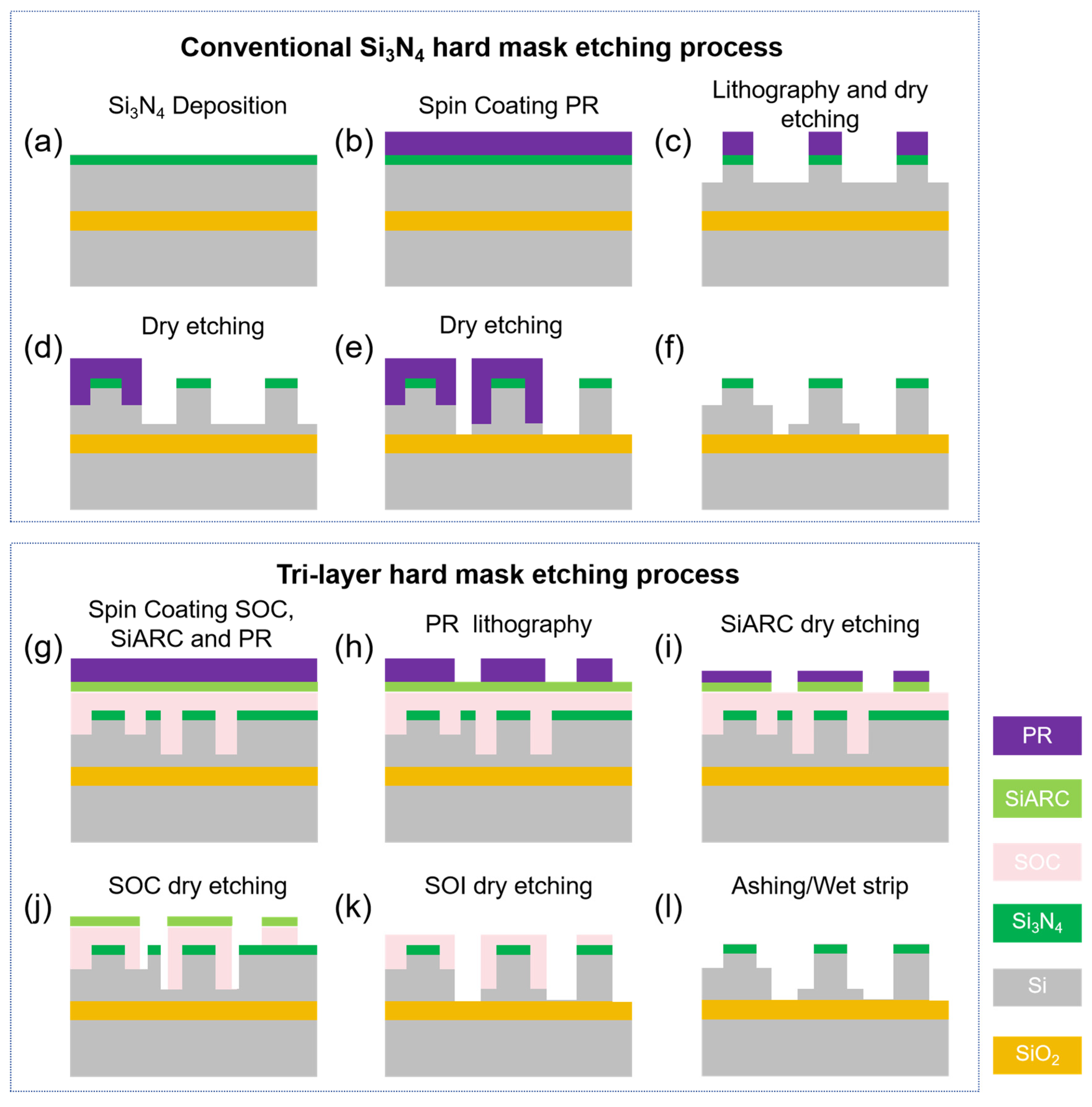
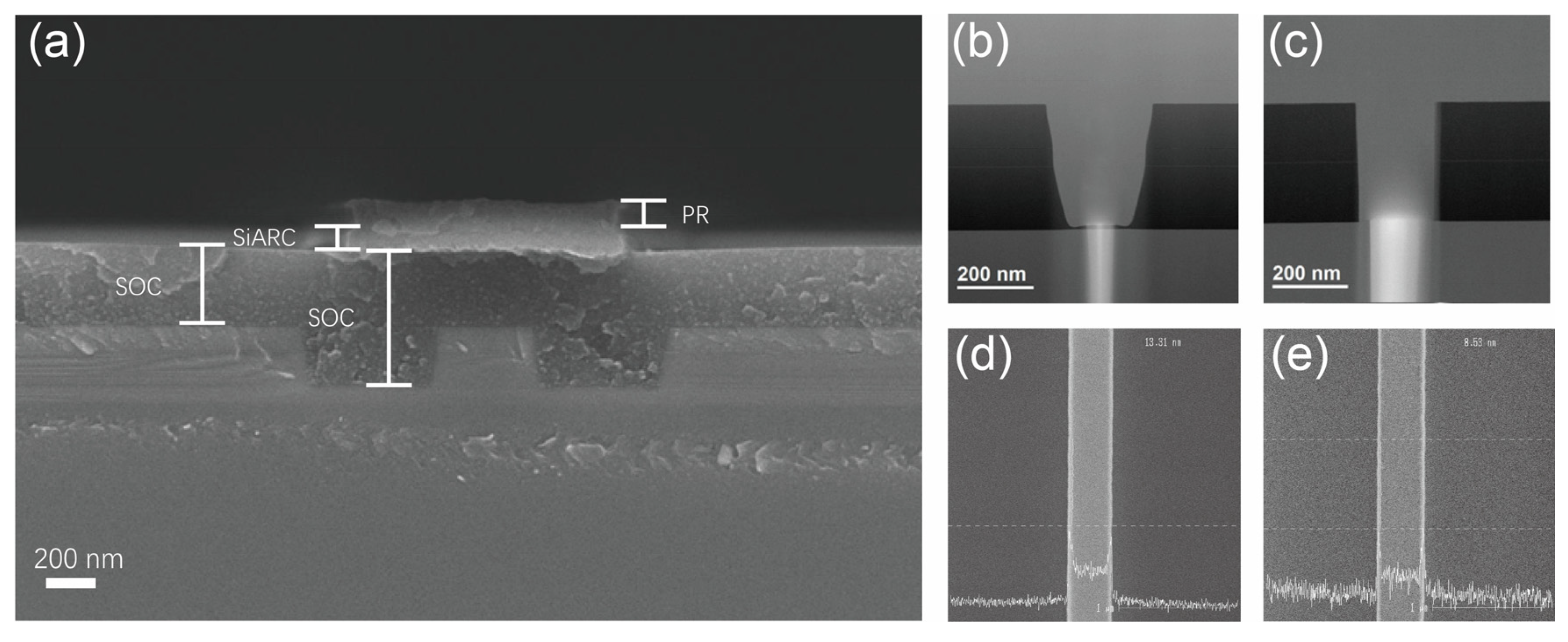
2. Tri-Layer Hard Mask Etching Process

Fabrication was performed on 200 mm silicon-on-insulator (SOI) wafers from SOITEC(Bernin, France) comprising a 220 nm thick single-crystal silicon device layer atop a 3 µm buried oxide (BOX) layer. Critical dimension and line-edge roughness (LER) measurements used CD-SEM (CG5000, Hitachi High-Tech Corporation, Tokyo, Japan) at 5 kV with 1 nm resolution. Propagation losses were quantified via the cutback method using a tunable laser source (81600B, Keysight Technologies, Santa Rosa, CA, USA), a polarization controller (Keysight N7786), an optical power meter (N7744A, Keysight Technologies, Santa Rosa, CA, USA), and a wafer prober (SUMMIT200, FormFactor, Inc., Livermore, CA, USA). TE-polarized light was injected into the waveguides. We designed two spiral waveguides with different lengths: a short waveguide (Lshort = 4 cm) and a long waveguide (Llong = 9 cm), with a length difference of 5 cm. The propagation loss α (in dB/cm) is calculated as:
α = P out L short P out L short / L long L short
where Pout(Lshort) and Pout(Llong) are the output powers for the short and long waveguides, respectively.
Figure 1a–f depict the flow schematics of the conventional Si3N4 hard mask process, where multiple etching steps typically induce a cumulative increase in the waveguide sidewall roughness, resulting in markedly enhanced optical scattering loss of waveguide propagation. Figure 1g–l illustrates the process flow of the tri-layer hard mask etching process proposed in this work, in which a SOC layer and a SiARC are sequentially deposited on both shallowly and deeply etched ridge waveguides. The cross-sectional SEM image of the SiARC layer after etching in the tri-layer hard mask process flow is shown in Figure 2a, in which the topmost region is photoresist (PR), with a thickness remaining of about 55 ± 3 nm after etching, and the bottom of the PR is 45 ± 2 nm thick SiARC. Since there is still a residue of PR, it effectively defines and preserves the SiARC layer, which is conducive to using SiARC as a mask layer for the subsequent etching process. The thicknesses of the SOC layer in different regions are 323 ± 16 nm (left side) and 540 ± 27 nm (half-etched waveguide region), respectively, and it exhibits thickness variations in different locations. This difference is due to the uneven bottom caused by the half-etched waveguide, and the SOC acts as a hard mask to fill in the bottom area, effectively transferring the pattern and maintaining mechanical stability. Overall, the interface between the photoresist and the SiARC layer, as well as the SOC layer, is clear, and the tri-layer hard mask etching process addresses a critical fabrication challenge, i.e., the flatness of the different waveguide regions.
Figure 2b and Figure 2c present the scanning electron microscopy (SEM) morphologies of the strip waveguides fabricated with the conventional Si3N4 hard mask and the tri-layer hard mask etching process, respectively. The former results in excessive angulation of the waveguide sidewalls and appears to visibly form depressions, which visually increase the roughness of the sidewalls. This may be due to the difference in the etching rate and selection ratio of the different etching steps, which may result in the formation of bumps or depressions at the junction. The latter results in the strip waveguide with flat and vertical sidewalls, and no significant shrinkage or sharp corners are observed. Figure 2d,e display the sidewall roughness of the 400 nm wide strip waveguide using critical dimension scanning electron microscopy (CDSEM) for both processes. The tri-layer hard mask etching process achieves a significant reduction in line-edge roughness of the strip waveguide compared to the conventional silicon nitride hard mask process, i.e., from 13.48 nm to 8.51 nm.
To comprehensively compare the effects of the conventional silicon nitride hard mask and tri-layer hard mask etching processes on waveguide propagation loss, wafer-level testing of the propagation loss of strip waveguides on a 200 mm SOI platform was targeted. The TE polarized light from a tunable laser was injected into waveguides with different lengths and the output was measured by an optical power meter. The famous cut back method was used to extract the unit propagation loss of the waveguide. Figure 3a and Figure 3d show the heat map of the propagation loss distribution at the 1311 nm wavelength on a 200 mm wafer (containing 26 chip regions) before and after waveguide process optimization, respectively. The histograms in Figure 3b,e further validate the median propagation loss before and after waveguide process optimization. The tri-layer hard mask etching process improves the median propagation loss from 2.35 dB/cm to 1.48 dB/cm. The tri-layer hard mask etching process produces lower strip silicon waveguide losses and a more uniform loss distribution. However, there are localized regions of higher loss at the periphery of the wafer, which may be related to the pattern mismatch due to the etching uniformity. In addition, the loss distributions and histograms of deeply etched ridge-type waveguides and shallowly etched ridge-type waveguides on wafers are also investigated, as shown in Figure S1. On the one hand, the waveguide loss under the tri-layer hard mask process is significantly better than that of the Si3N4 hard mask, with the median losses of 1.18 dB/cm and 0.29 dB/cm for the deep-ridged and shallow-etched ridge waveguides, respectively. On the other hand, the thermal map distribution shows that the deeply etched ridge-type waveguides also suffer from the similar problem of high localized loss, while the shallowly etched ridge-type waveguides do not have such a problem. Therefore, there is still room for optimization of the tri-layer hard mask process in terms of etching quality and mode conversion. In contrast, the uneven loss distribution exhibited by the Si3N4 hard mask etched strip silicon waveguide should originate from the limitations of the deep etching process, which makes it difficult to achieve consistent process control across the entire wafer range, leading to small etch depth differences in different regions. Figure 3c and Figure 3f show the spectral results of the propagation loss of the strip silicon waveguide fabricated using the two processes, respectively. Compared with the conventional Si3N4 hard mask process, the tri-layer hard mask etching process achieves lower propagation loss in the wavelength range of 1260–1340 nm, especially in the short wavelength range of 1260–1280 nm. In the wavelength range of 1280–1300 nm, the loss of the strip waveguide is typically higher, but the tri-layer hard mask etching process still achieves a 30–40% reduction compared to the Si3N4 mask process. Therefore, combined with the optimization results of the tri-layer hard mask Si3N4 process for line-edge roughness and propagation loss, the process excels in reducing scattering loss, increasing pattern stability, and improving fabrication uniformity, making it particularly suitable for broadband low-loss propagation applications.

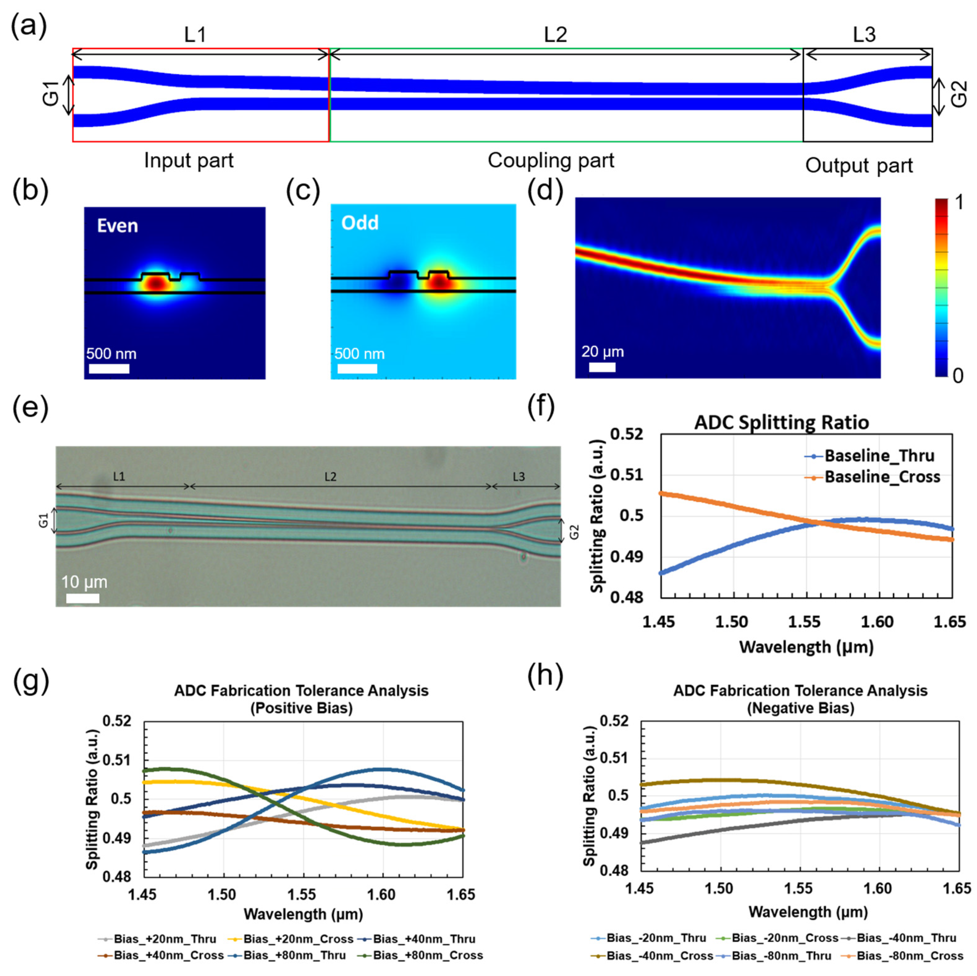
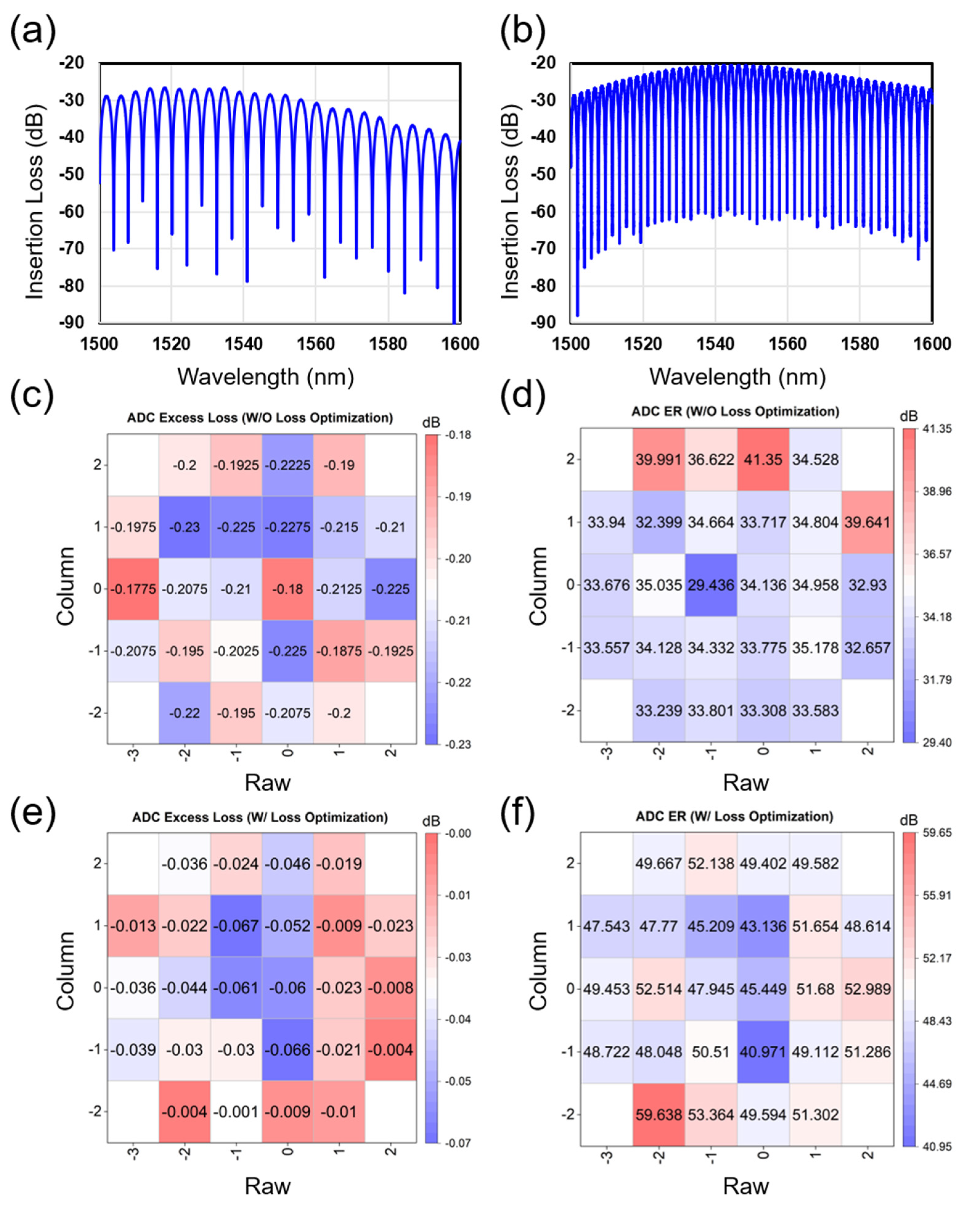
3. Adiabatic Directional Couplers

According to the results discussed above, the tri-layer hard mask technique can not only significantly reduce the sidewall roughness of silicon waveguides, but also can realize perfectly flat and vertical profiles of the waveguide cross-section. One should expect a certain excess loss reduction since the length of ADC is generally large. In addition, the ideal geometrical profile will suppress the unwanted supermodes coupling as designed, which will ensure a balanced splitting ratio for the fabricated ADC. To validate the effectiveness of tri-layer hard mask technology on the fundamental silicon photonics component, we designed and fabricated adiabatic directional couplers (ADCs) on the 200 mm SOI platform.
The schematic structure of the proposed low-loss waveguide-based ADC is depicted in Figure 4a. Generally, an ADC is composed of three parts, i.e., an input part, coupling part, and output part. The coupling part contains two waveguides whose widths are slowly changed from the left side to the right side. Such a structure can be treated as a supermode waveguide system. The coupling part should be judiciously designed to suppress the coupling between the supermodes supported by the waveguide system to ensure a low insertion loss and balanced splitting ratio performance. The supermodes coupling intensity can be expressed as follows:
Ω = m n | 0 1 κ m n z e j L 0 L | β m s β n s | d s d z | 2
where L is the coupling length, β m z and β n z are the complex propagation constant of supermode m and n, and κ m n is the localized coupling coefficient of mode m and n,
κ m n z = ω 4 1 β m z β n z E ¯ m * ε z E ¯ n d x d y
where ω is the angular frequency, E ¯ m and E ¯ n are the electrical field of supermode m and n, and ε is the complex dielectric constant. To realize a minimum coupling coefficient κ m n , the difference between β m z and β n z should be designed as relatively large. Following the general rule discussed above, the optimized parameters of the ADC are as follows: G1 and G2 are 7.4 μm and 7.5 μm, and L1, L2, and L3 are 60 μm, 150 μm, and 40 μm, respectively. The input and output waveguide widths are fixed at 0.5 μm. The upper waveguide tapers from 0.5 μm to 0.8 μm in the input part and then tapers from 0.8 μm to 0.4 μm in the coupling part. The lower waveguide tapers from 0.5 μm to 0.4 μm in the input part and then remains constant in the coupling part. For the output part, both waveguides taper from 0.4 μm to 0.5 μm.
Figure 4b,c depict the electric field distribution of the 1st and 2nd supermodes of the waveguide system. The cross-section is chosen to be the left port of the coupling part. The even mode corresponds to the 1st supermode, and the odd mode corresponds to the 2nd supermode. The electric field of these two modes are quite different as a result of our dedicated design. Figure 4d illustrates the static optical intensity propagation when light is injected from the upper waveguide at the left port of input part of the designed ADC. Apparently, a balanced optical intensity output is observed at the ADC right output ports. Figure 4e shows a micrograph of an ADC based on a low-loss waveguide process. Figure 4f shows the simulated splitting ratio between the two ADC ports. The splitting ratio of both ports of this ADC is within 3 dB ± 0.2 dB in the range of 200 nm from 1450 nm to 1650 nm, and 3 dB ± 0.15 dB in the range of 100 nm from 1500 nm to 1600 nm. Figure 4g,h show the simulation analysis of the processing tolerance of the ADC, demonstrating negligible degradation even with ±80 nm waveguide width variations.
To test the splitting ratio of ADC, a cascaded ADC Mach–Zehnder interference (MZI) structure is designed in this paper. The MZI structure consisted of two cascaded ADCs connected by two arms of different length. The length differences resulted in interference fringes as shown in Figure 5a,b. Since the length differences are 140 μm and 308 μm, so the free spectral range (FSR) of the interference fringes in Figure 5a,b are slightly different. However, one should note that such a difference will not affect the splitting ratio evaluation. By testing the ER of the interference structure, the spectral ratio of the ADC can be deduced. The relationship between the ER and splitting ratio can be derived as follows:
20 log 10 ( a + b a b ) = E R
where a and b are the splitting ratio and a + b = 1.
Figure 5 compares the performance of ADC with and without waveguide loss optimization. Figure 5a,b show the typical interference optical spectrum of ADC without and with waveguide loss optimization. The ER is improved from 30 dB to 40 dB in the range of 100 nm from 1500 nm to 1600 nm, which means the splitting ratio is improved from 3 dB ± 0.28 dB to 3 dB ± 0.15 dB. Figure 5c,e compare the excess loss wafer map of ADC without and with waveguide loss optimization. The excess loss is improved from -0.23 dB to larger than −0.067 dB. As shown in Figure 5d,f, after waveguide loss optimization, the extinction ratio values range from 40.971 dB to 53.638 dB, and the difference in extinction ratios at each position is reduced.
Table 1 summarizes the performance of state-of-the-art 3 dB adiabatic couplers. While the device size of this work is not minimal, it achieves an excellent beam splitting ratio and sufficiently low additional loss given the smaller size. The advantages of the low-loss waveguide process for the comprehensive performance enhancement of ADC devices are fully demonstrated, which is highly valuable and promising for applications in the fields of large-scale, multistage optical switching arrays and optical neural networks.

4. Conclusions

Silicon photonics has long been constrained by waveguide losses dominated by sidewall roughness, limiting the performance and scalability of photonic integrated circuits. In this work, we introduce a tri-layer hard mask etching process that overcomes this limitation by enabling ultralow-loss silicon waveguides and high-performance photonic devices. By integrating SOC, SiARC, and photoresist layers, the tri-layer hard mask etching process achieves precise control over sidewall profiles, reducing line-edge roughness to 8.51 nm and waveguide propagation loss to 1.48 dB/cm. This advancement stems from enhanced etching uniformity, minimized scattering losses, and improved mechanical stability during fabrication. The tri-layer hard mask etching process proves capable of achieving high performance and fabrication tolerance for one elementary silicon photonics component, i.e., ADCs. The fabricated ADCs achieve a near-ideal splitting ratio of 3 dB ± 0.15 dB with only 0.067 dB excess loss. These devices demonstrate exceptional wavelength insensitivity, fabrication tolerance, and compactness, addressing critical limitations of existing splitters in terms of loss, footprint, and operational bandwidth.

Supplementary Materials

The following supporting information can be downloaded at: https://www.mdpi.com/article/10.3390/nano15120947/s1. Figure S1: Propagation losses in deeply etched ridge-type and shallowly etched ridge-type waveguides.

Author Contributions

K.Z.: project administration, supervision, funding acquisition, conceptualization, data curation, investigation, methodology, writing—original draft. Y.Y.: data curation, investigation. N.Z.: data curation, investigation. S.Z.: data curation, investigation. J.S.: data curation, investigation. S.D.: supervision, writing—review and editing. D.W.Z.: supervision, writing—review and editing. All authors have read and agreed to the published version of the manuscript.

Funding

This work is primarily supported by K.Z.’s personal funds and resources, through Silith Technology Co., Ltd.

Data Availability Statement

The data presented in this study are available on request from the corresponding author.

Conflicts of Interest

Authors Ke Zhang, Yunchu Yu, Nanfei Zhu, Senlin Zhang, Jie Sun are employed by the company Silith Technology Co., Ltd. The remaining authors declare that the research was conducted in the absence of any commercial or financial relationships that could be construed as a potential conflict of interest. The funder was not involved in the study design, collection, analysis, interpretation of data, the writing of this article or the decision to submit it for publication.

References

  1. Shi, Y.C.; Zhang, Y.; Wan, Y.T.; Yu, Y.; Zhang, Y.G.; Hu, X.; Xiao, X.; Xu, H.G.; Zhang, L.; Pan, B.C. Silicon photonics for high-capacity data communications. Photonics Res. 2022, 10, A106–A134. [Google Scholar] [CrossRef]
  2. Pitris, S.; Moralis-Pegios, M.; Alexoudi, T.; Ban, Y.; Heyn, P.D.; Campenhout, J.V.; Lambrecht, J.; Ramon, H.; Yin, X.; Bauwelinck, J.; et al. O-band silicon photonic transmitters for datacom and computercom interconnects. J. Light. Technol. 2019, 37, 5140–5148. [Google Scholar] [CrossRef]
  3. Hong, S.; Zhang, L.; Wang, Y.; Zhang, M.; Xie, Y.W.; Dai, D.X. Ultralow-loss compact silicon photonic waveguide spirals and delay lines. Photonics Res. 2021, 10, 1–7. [Google Scholar] [CrossRef]
  4. Lu, Z.Q.; Yun, H.; Wang, Y.; Chen, Z.T.; Zhang, F.; Jaeger, N.A.F.; Chrostowski, L. Broadband silicon photonic directional coupler using asymmetric-waveguide based phase control. Opt. Express 2015, 23, 3795–3808. [Google Scholar] [CrossRef]
  5. Zhou, Y.; Sun, Y.H.; Wu, H.Y.; Lu, M.J.; Hu, G.H.; Yun, B.F.; Cui, Y.P. A low loss silicon waveguide bend based on width and curvature variations. Opt. Commun. 2024, 565, 130679. [Google Scholar] [CrossRef]
  6. Cardenas, J.; Poitras, C.B.; Robinson, J.T.; Preston, K.; Chen, L.; Lison, M. Low loss etchless silicon photonic waveguides. Opt. Express 2009, 17, 4752–4757. [Google Scholar] [CrossRef]
  7. Wang, X.Y.; Zhou, L.J.; Li, R.F.; Xie, J.Y.; Lu, L.J.; Wu, K.; Chen, J.P. Continuously tunable ultra-thin silicon waveguide optical delay line. Optica 2017, 4, 507–515. [Google Scholar] [CrossRef]
  8. Lee, K.K.; Lim, D.R.; Kimerling, L.C.; Shin, J.; Cerrina, F. Fabrication of ultralow-loss Si/SiO2 waveguides by roughness reduction. Opt. Lett. 2001, 26, 1888–1890. [Google Scholar] [CrossRef] [PubMed]
  9. Gao, F.; Wang, Y.; Cao, G.; Jia, X.; Zhang, F. Improvement of sidewall surface roughness in silicon-on-insulator rib waveguides. Appl. Phys. B 2005, 81, 691–694. [Google Scholar] [CrossRef]
  10. Bellegarde, C.; Pargon, E.; Sciancalepore, C.; Petit-Etienne, C.; Hugues, V.; Robin-Brosse, D.; Hartmann, J.M.; Lyan, P. Improvement of sidewall roughness of submicron SOI waveguides by hydrogen plasma and annealing. IEEE Photonics Technol. Lett. 2018, 30, 591–594. [Google Scholar] [CrossRef]
  11. Dong, P.; Qian, W.; Liao, S.; Liang, H.; Kung, C.C.; Feng, N.N.; Shafiiha, R.; Fong, J.; Feng, D.; Krishnamoorthy, A.V. Low loss shallow-ridge silicon waveguides. Opt. Express 2010, 18, 14474–14479. [Google Scholar] [CrossRef] [PubMed]
  12. Pafchek, R.; Tummidi, R.; Li, J.; Webster, M.; Chen, E.; Koch, T. Low-loss silicon-on-insulator shallow-ridge TE and TM waveguides formed using thermal oxidation. Appl. Opt. 2009, 48, 958–963. [Google Scholar] [CrossRef] [PubMed]
  13. Liu, X.; Zhao, Y.; Gan, F. Ultra-broadband, Fabrication-tolerant 3-dB Power Splitter Based on Dual-layer SOI Platform. In Proceedings of the 2024 IEEE Silicon Photonics Conference (SiPhotonics), Tokyo Bay, Japan, 15–18 April 2024; pp. 1–2. [Google Scholar] [CrossRef]
  14. Sun, S.; He, M.; Xu, M.; Cai, X. Hybrid silicon and lithium niobate modulator. IEEE J. Sel. Top. Quantum Electron. 2020, 27, 1–12. [Google Scholar] [CrossRef]
  15. Chen, S.T.; Shi, Y.C.; He, S.L.; Dai, D.X. Low-loss and broadband 2 × 2 silicon thermo-optic Mach–Zehnder switch with bent directional couplers. Opt. Lett. 2016, 41, 836–839. [Google Scholar] [CrossRef]
  16. Deng, Q.Z.; El-Saeed, A.H.; Elshazly, A.; Lepage, G.; Marchese, C.; Kobbi, H.; Magdziak, R.; Coster, J.D.; Singh, N.; Filipcic, M.E.; et al. 32 × 100 GHz WDM filter based on ultra-compact silicon rings with a high thermal tuning efficiency of 5.85 mW/π. In Proceedings of the Optical Fiber Communication Conference, San Diego, CA, USA, 24–28 March 2024; Optica Publishing Group: Washington, DC, USA, 2024. W1A. 3. [Google Scholar]
  17. Qiao, L.; Tang, W.; Chu, T. 32 × 32 silicon electro-optic switch with built-in monitors and balanced-status units. Sci. Rep. 2017, 7, 42306. [Google Scholar] [CrossRef]
  18. Shen, Y.C.; Harris, N.C.; Skirlo, S.; Prabhu, M.; Jones, T.B.; Hochberg, M.; Sun, X.; Zhao, S.J.; Larochelle, H.; Englund, D.; et al. Deep learning with coherent nanophotonic circuits. Nat. Photonics 2017, 11, 441–446. [Google Scholar] [CrossRef]
  19. Hu, M.H.; Huang, J.Z.; Scarmozzino, R.; Levy, M.; Osgood-Jr, R.M. A low-loss and compact waveguide Y-branch using refractive-index tapering. IEEE Photonics Technol. Lett. 1997, 9, 203–205. [Google Scholar] [CrossRef]
  20. Gupta, R.K.; Chandran, S.; Das, B.K. Wavelength-independent directional couplers for integrated silicon photonics. J. Light. Technol. 2017, 35, 4916–4923. [Google Scholar] [CrossRef]
  21. Liu, R.F.; Lu, L.H.; Zhang, P.J.; Chang, W.J.; Liu, D.M.; Zhang, M.M. Integrated dual-mode 3-dB power splitter based on multimode interference coupler. IEEE Photonics Technol. Lett. 2020, 32, 883–886. [Google Scholar] [CrossRef]
  22. Chen, W.W.; Lin, J.; Li, H.X.; Wang, P.J.; Dai, S.X.; Liu, Y.X.; Yao, R.K.; Li, J.; Qiang, F.; Dai, T.G.; et al. Broadband multimode 3 dB optical power splitter using tapered couplers. Opt. Express 2022, 30, 46236–46247. [Google Scholar] [CrossRef]
  23. Kim, H.; Shin, H. Tailorable and broadband on-chip optical power splitter. Appl. Sci. 2019, 9, 4239. [Google Scholar] [CrossRef]
  24. Halir, R.; Maese-Novo, A.; Ortega-Moñux, A.; Molina-Fernández, I.; Wangüemert-Pérez, J.G.; Cheben, P.; Xu, D.X.; Schmid, J.H.; Janz, S. Colorless directional coupler with dispersion engineered sub-wavelength structure. Opt. Express 2012, 20, 13470–13477. [Google Scholar] [CrossRef] [PubMed]
  25. Han, L.S.; Kuo, B.P.P.; Alic, N.; Radic, S. Ultra-broadband multimode 3dB optical power splitter using an adiabatic coupler and a Y-branch. Opt. Express 2018, 26, 14800–14809. [Google Scholar] [CrossRef] [PubMed]
  26. Mao, D.; Wang, Y.; El-Fiky, E.; Xu, L.H.; Kumar, A.K.; Jacques, M.; Samani, A.; Carpentier, O.; Bernal, S.; Alam, M.S.; et al. Adiabatic coupler with design-intended splitting ratio. J. Light. Technol. 2019, 37, 6147–6155. [Google Scholar] [CrossRef]
  27. Xing, J.J.; Xiong, K.; Xu, H.; Li, Z.Y.; Xiao, X.; Yu, J.Z.; Yu, Y. Silicon-on-insulator-based adiabatic splitter with simultaneous tapering of velocity and coupling. Opt. Lett. 2013, 38, 2221–2223. [Google Scholar] [CrossRef]
  28. Staaks, D.; Hsu, Y.; Lee, K.Y.; Steiner, P.L.; Yu, Z.N.; Wu, J.J.; Xiao, S.G.; Yang, X.M.; Chang, T.Y. Nanoimprint lithography guiding templates for advanced magnetic media fabrication. J. Vac. Sci. Technol. B 2024, 42, 013801. [Google Scholar] [CrossRef]
  29. Nakajima, M.; Allen, R.D.; Somervell, M.H.; Kanno, Y.; Shibayama, W.; Takeda, S.; Kato, M.; Matsumoto, T. Development of new Si-contained hardmask for tri-layer process. In Advances in Resist Materials & Processing Technology XXVIII; International Society for Optics and Photonics: Bellingham, WA, USA, 2011; 797225. [Google Scholar]
  30. Shibayama, W.; Shigaki, S.; Sakamoto, R.; Onishi, R.; Bang, C.H. EUV sensitive Si containing hard mask (Si-HM) for PTD and NTD process in EUVL. In Proceedings of the Spie Advanced Lithography, San Jose, CA, USA, 24–28 February 2013. [Google Scholar]
  31. Liu, X.; Sheng, Z.; Zhao, Y.X.; Gan, F.W. Ultra-broadband on-chip power splitters for arbitrary ratios on silicon-on-insulator. Opt. Express 2024, 32, 2029–2038. [Google Scholar] [CrossRef]
  32. Liu, X.; Zhao, Y.X.; Sheng, Z.; Gan, F.W. Compact and ultra-broadband silicon photonic adiabatic directional coupler using rib waveguides. IEEE Photonics Technol. Lett. 2024, 36, 637–640. [Google Scholar] [CrossRef]
  33. Guo, D.F.; Tao, C. Compact broadband silicon 3 dB coupler based on shortcuts to adiabaticity. Opt. Lett. 2018, 43, 4795–4798. [Google Scholar] [CrossRef]
  34. Hung, Y.J.; Li, Z.Y.; Chung, H.C.; Liang, F.C.; Jung, M.Y.; Yen, T.H.; Tseng, S.Y. Mode-evolution-based silicon-on-insulator 3 dB coupler using fast quasiadiabatic dynamics. Opt. Lett. 2019, 44, 815–818. [Google Scholar] [CrossRef]
  35. Tamazin, H.; El-Fiky, E.; Wang, Y.; D’Mello, Y.; Patel, D.; Kumar, A.K.; Plant, D.V. Ultra-broadband compact adiabatic coupler in silicon-on-insulator for joint operation in the C-and O-bands. In Proceedings of the CLEO: Science and Innovations, San Jose, CA, USA, 13–18 May 2018; Optica Publishing Group: Washington, DC, USA, 2018. [Google Scholar]
  36. Cabanillas, J.M.F.; Popović, M.A. Fast adiabatic mode evolution based on geometry-induced suppression of nearest-mode crosstalk. In Proceedings of the Conference on Lasers and Electro-Optics, San Jose, CA, USA, 13–18 May 2018; pp. 1–2. [Google Scholar]
Figure 1. (af) Schematic diagram of conventional Si3N4 hard mask etching process. (gl) Schematic diagram of tri-layer hard mask etching process.
Nanomaterials 15 00947 g001
Figure 2. (a) Cross-sectional SEM image of a half-etched ridge-type waveguide after etching the SiARC layer in a tri-layer hard mask process flow. (b) Cross-sectional SEM photographs of a strip waveguide prepared by a conventional Si3N4 hard mask process. (c) Cross-sectional SEM photographs of strip waveguides prepared by tri-layer hard mask process. (d) CDSEM results of a strip waveguide prepared by a conventional Si3N4 hard mask process. (e) CDSEM results of a strip waveguide prepared by tri-layer hard mask process.
Nanomaterials 15 00947 g002
Figure 3. (a) Thermal map of waveguide loss distribution at 1311 nm for strip waveguides fabricated using conventional Si3N4 hard mask process. (b) Histogram of waveguide propagation loss under conventional Si3N4 hard mask process. (c) Plot of propagation loss versus wavelength for strip waveguides using conventional Si3N4 hard mask process. (d) Thermal map of waveguide loss distribution at 1311 nm for strip waveguides fabricated using tri-layer hard mask process. (e) Histogram of waveguide propagation loss under tri-layer hard mask process. (f) Plot of propagation loss versus wavelength for strip waveguides using tri-layer hard mask process. M and S are abbreviations for median and standard deviation, respectively. (x,y) represents the die at the xth row and yth column position on the wafer.
Nanomaterials 15 00947 g003
Figure 4. (a) Schematic view of ADC coupler design. (bd) Simulated electric field distributions for the wavelength of 1550 nm, when the light is launched into Input 1: (b) even; (c) odd and (d) top view. (e) Optical micrograph of the ADC. (f) Simulated ADC splitting ratio. (g,h) Simulated splitting ratios versus wavelength for different coupler lengths.
Nanomaterials 15 00947 g004
Figure 5. Tested results of ADC without loss optimization: (a) optical interference spectrum; (c) excess loss wafer map; and (d) ER wafer map. Those of ADC with loss optimization: (b) optical interference spectrum; (e) excess loss wafer map; and (f) ER wafer map.
Nanomaterials 15 00947 g005
Table 1. Comparison of the performance of our device with previously reported silicon photonics 2 × 2 3 dB adiabatic couplers. RAC: rapid adiabatic coupler.
TypeYearSplitting RatioExcess Loss (dB)Device Length
(μm)
ADC [31]20240.563:0.4370.2279
ADC [32]20240.538:0.4620.18108
ADC [26]20210.53:0.47NR110
ADC [33]20180.52:0.480.370
ADC [34]20190.56:0.44NR26.3
ADC [35]20180.533:0.467NR100
ADC [27]20130.51:0.490.3300
RAC [36]20180.51:0.49NRNR
This Work0.516:0.4840.06789
Disclaimer/Publisher’s Note: The statements, opinions and data contained in all publications are solely those of the individual author(s) and contributor(s) and not of MDPI and/or the editor(s). MDPI and/or the editor(s) disclaim responsibility for any injury to people or property resulting from any ideas, methods, instructions or products referred to in the content.

