1. Introduction
Since the discovery of graphene, van der Waals (vdWs) materials have garnered increasing interest in the scientific community due to their potential applications, with particular attention directed toward transition metal dichalcogenides (TMDs) [
1,
2]. TMDs have demonstrated significant potential in photodetector applications, especially in terms of their outstanding performance in photoelectric conversion and detection efficiency [
3,
4,
5,
6]. In recent years, breakthroughs in material preparation and fabrication techniques have led to continuous improvements in the optoelectronic properties of TMDs, positioning them as an emerging research focus in the field of optoelectronics [
7,
8,
9].
Molybdenum diselenide (MoSe
2), a representative vdWs layered material, possesses notable structural and electronic characteristics [
10]. Structurally, monolayer MoSe
2 exhibits a sandwich-like configuration with a thickness of approximately 0.65 nm, as shown in
Figure 1a. Electronically, it displays pronounced quantum confinement effects [
11,
12]. First principle calculations based on the density functional theory (DFT), incorporating the generalized gradient approximation and spin–orbit coupling (SOC), reveal that monolayer MoSe
2 possesses a direct bandgap of approximately 1.5 eV. In contrast, this bandgap reduces to around 1.1 eV in the bulk form, indicating a layer-dependent bandgap tunability that opens avenues for band structure engineering [
13,
14]. Moreover, the absence of dangling bonds on the MoSe
2 surface provides a unique advantage in constructing heterostructures. When combined with its intrinsic physical and chemical stability, this feature underscores the material’s potential in photodetectors and flexible electronic sensors [
15].
However, due to its intrinsic bandgap, the photoresponse of MoSe
2 films in the mid-infrared (MIR) spectral range is nearly negligible, which severely limits its applications. Eliminating the limitations imposed by the bandgap to enable efficient photoelectric response beyond the intrinsic absorption range of vdWs materials has become a pressing research challenge. An innovative strategy to address this issue lies in leveraging localized surface plasmon resonance (LSPR) effects induced by metasurfaces [
16,
17,
18,
19]. By engineering metallic nanostructures, strong localized electromagnetic fields can be generated at specific wavelengths. These fields, through near-field coupling or carrier transfer mechanisms, can extend the photoresponse of materials beyond their inherent absorption spectrum, thereby opening new pathways for the functional enhancement of optoelectronic systems [
20,
21,
22].
In this work, we report a precursor selenization method for the fabrication of large-area, high-quality MoSe2 films. Furthermore, we propose the integration of Au-based metasurfaces with MoSe2 films to construct a photoconductive Schottky junction detector. By harnessing the LSPR effect of Au nanostructures to generate hot electron injection, this approach effectively overcomes the intrinsic bandgap limitation of MoSe2, thereby enabling highly sensitive detection of MIR optical signals. The responsivity and specific detection rate of this device are 7.1 mA/W and 1.12 × 10⁸ Jones at a wavelength of 4 μm. Furthermore, this device has a wide spectral response, ranging from 808 nm to 10 μm. This study not only introduces a novel mechanism for enhancing the photoelectric response of vdWs materials beyond their intrinsic absorption spectrum, but also opens up a new pathway for the design of cost-effective, room-temperature MIR detectors.
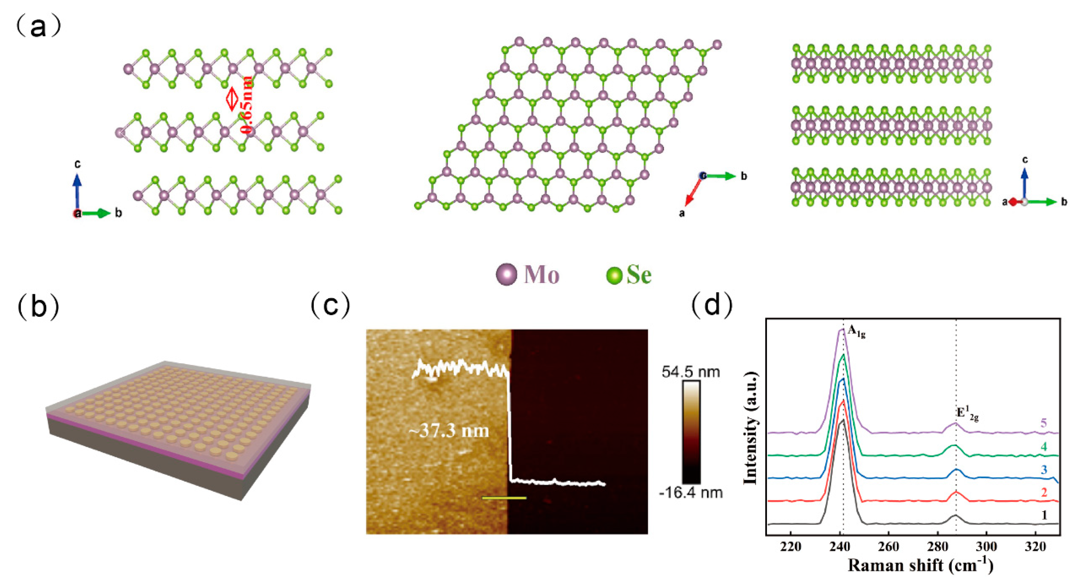
Figure 1.
MoSe
2 and device structure. (
a) Top and side views of the monoclinic structure of MoSe
2. (
b) Schematic diagram of a metasurface-enhanced MoSe
2 photodetector. (
c) AFM image of a MoSe
2 thin film with a measured thickness of approximately 37.3 nm. (
d) Raman spectra of MoSe
2 measured at five marked positions in
Figure 2a.
Figure 2.
Structural characterization of MoSe2 thin films. (a) A 4 cm × 4 cm MoSe2 film on quartz. (b) and (c) Raman mapping images of the MoSe2 thin film obtained within an area of 100 μm × 100 μm. (d) The XPS spectra and (e) XRD patterns of the MoSe2 film. (f) HRTEM and the corresponding FFT images of MoSe2.
3. Results and Discussion
To evaluate the surface morphology, sample quality, and composition of the synthesized MoSe
2 films, various techniques were employed to analyze the films. As shown in
Figure 2a, the large-area MoSe
2 film fabricated via the selenization method exhibited a uniform color on a 4 cm × 4 cm quartz substrate. Raman spectroscopic analysis (
Figure 1d) was performed at five representative points across the sample surface, along with Raman mapping over a 100 μm × 100 μm region provided in
Figure 2b,c. The results reveal highly consistent spectral features across all measured regions. Notably, two prominent characteristic peaks located at 240.3 cm
−1 and 288.1 cm
−1 correspond to the out-of-plane (
) and in-plane (
) vibrational modes of MoSe
2, respectively. This high degree of spectral uniformity strongly confirms the excellent homogeneity of the synthesized film.
In
Figure 2d, X-ray photoelectron spectroscopy (XPS) analysis of the MoSe
2 film reveals distinct peaks at binding energies of 228.5 eV and 231.7 eV, corresponding to the Mo 3d
5/2 and Mo 3d
3/2 orbitals, respectively. Additionally, a doublet observed at 54.6 eV and 55.4 eV is attributed to the Se 3d
5/2 and Se 3d
3/2 orbitals. The presence and relative intensities of these characteristic peaks confirm the stoichiometry of the synthesized film as MoSe
2. Importantly, no significant impurity-related peaks were detected, indicating a high degree of chemical purity in the sample. As shown in
Figure 2e, the X-ray diffraction (XRD) pattern of the film was compared with the standard reference card (PDF#65-3481). Distinct diffraction peaks were observed at 13.7°, 42.1°, and 57.1°, which correspond to the (002), (006), and (008) planes of the MoSe
2 crystal, respectively. These results confirm that the film possesses a MoSe
2 phase with high crystallinity and evident preferential orientation, highlighting the structural quality of the synthesized material.
As demonstrated in
Figure 2f, high-resolution transmission electron microscopy (HRTEM) imaging coupled with fast Fourier transform (FFT) diffraction analysis confirms that the MoSe
2 film adopts a monoclinic crystal structure. The observed lattice spacings of 0.28 nm correspond to the (100) crystal planes, respectively. The electrical properties of the MoSe
2 film were further investigated using a Hall effect measurement system. For a film thickness of 40 nm, the resistivity was measured to be 0.107 Ω·cm, and the carrier mobility reached 8.27 cm
2·V
−1·s
−1. These structural and electrical characterizations collectively confirm the successful synthesis of high-quality 2D MoSe
2 films.
The metasurface-enhanced MoSe
2 photodetector, as illustrated in
Figure 1b, features a hybrid architecture composed of a MoSe
2 film integrated with circular plasmonic resonators. The subwavelength design of the metasurface is tailored to match the wavelength of the incident light, enabling the excitation of both surface plasmon polaritons (SPPs) and LSPR. These plasmonic effects result in a strong confinement and concentration of optical energy near the material surface, thereby enhancing the local electromagnetic field. A Schottky junction is formed between the Au metasurface and the MoSe
2 layer. At resonant wavelengths, the LSPR effect of the Au nanostructures facilitates hot electron injection into the MoSe
2, effectively overcoming the limitations imposed by its intrinsic bandgap. This mechanism enables enhanced optical absorption and improved photoelectric conversion efficiency, particularly in spectral regions beyond the native absorption range of MoSe
2.
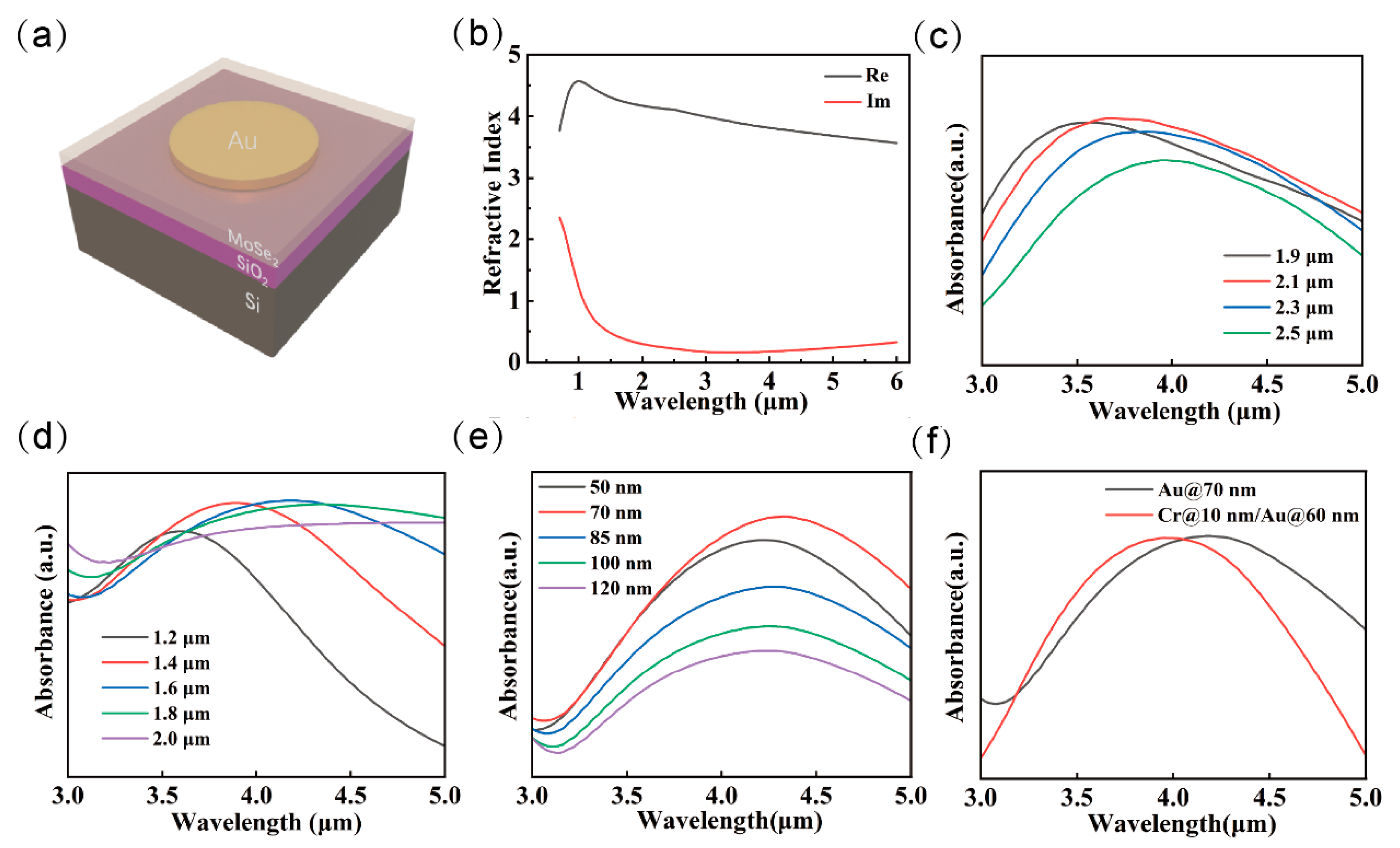
To investigate the optical absorption characteristics of the designed plasmonic structure, finite-difference time-domain (FDTD) simulations were conducted, and the key structural parameters were systematically optimized.
Figure 3a presents the schematic of the single-period unit cell configuration set within the simulation software. Based on the approximate resonance condition
SPR ≈ 2
neff, the disk diameter was initially estimated to achieve resonance at the 4 μm wavelength. Subsequently, the effects of metasurface parameters, such as disk diameter and periodicity, on the absorption performance were analyzed through iterative simulations and structural refinements. This optimization process allowed for precise tuning of the plasmonic resonance behavior to maximize optical absorption at the desired spectral position.
When varying the thickness of the metasurface (
Figure 3e), distinct absorption behaviors are observed. At a thickness of 50 nm, the metal layer approaches the mean free path of electrons (~40 nm), which enhances surface roughness scattering. Moreover, the film is insufficiently thick to fully confine the electromagnetic field, resulting in increased energy leakage into the substrate or enhanced radiative losses, thereby leading to a relatively low absorption efficiency. At a thickness of 70 nm, the metal layer exceeds three times the skin depth of Au at a 4 μm wavelength (approximately ~20 nm), enabling strong localization of the electromagnetic field. At this point, Ohmic losses have not yet surpassed radiative losses significantly, allowing for the maximization of absorption efficiency. However, further increasing the thickness leads to a dominant contribution from Ohmic losses. An excessively thick metal layer introduces impedance mismatch, which can increase reflection and suppress the efficient excitation of plasmonic resonance modes—such as via cutoff effects in waveguide-like structures—thereby reducing the overall absorption rate.
The observed broadening of the absorption peak with increasing disk diameter, as shown in
Figure 3c, primarily arises from the excitation of higher-order multipolar modes and the enhancement of radiative losses. When the disk diameter approaches or exceeds half the effective wavelength (
D ≥
λ/2
neff), the nano-disk supports not only the fundamental dipolar mode but also higher-order resonances such as quadrupole and magnetic dipole modes. The spectral overlap and superposition of these resonant modes lead to the merging of multiple peaks, resulting in a broadened absorption bandwidth. Moreover, larger structures introduce more radiative decay channels, allowing energy to leak out via enhanced scattering and diffraction. This increased radiative loss reduces the resonance quality factor (Q-factor) and increases the full width at half maximum (FWHM) of the absorption peak. These effects collectively contribute to the broadband absorption characteristics of the plasmonic metasurface.
The redshift of the absorption peak observed with increasing metasurface periodicity is primarily attributed to the change in lattice resonance conditions. For a given period
P, the resonance wavelength
approximately satisfies the relationship
, where
is the effective refractive index of the metasurface. At smaller periods (e.g., 1.9 μm), the subwavelength spacing between neighboring unit cells leads to stronger near-field coupling. This enhanced coupling facilitates the excitation of collective resonance modes with stronger energy localization, resulting in higher absorption efficiency. However, as the period increases and the unit spacing exceeds the near-field interaction range (typically on the order of the wavelength), the coupling efficiency declines. Consequently, the collective resonances degrade into localized resonances of individual nanostructures, with increased radiative losses and reduced absorption. Moreover, when the period
, higher-order diffraction channels (e.g., m = ±1) become accessible. These channels allow partial energy to escape via diffraction, further lowering the absorption efficiency, as illustrated in
Figure 3b.
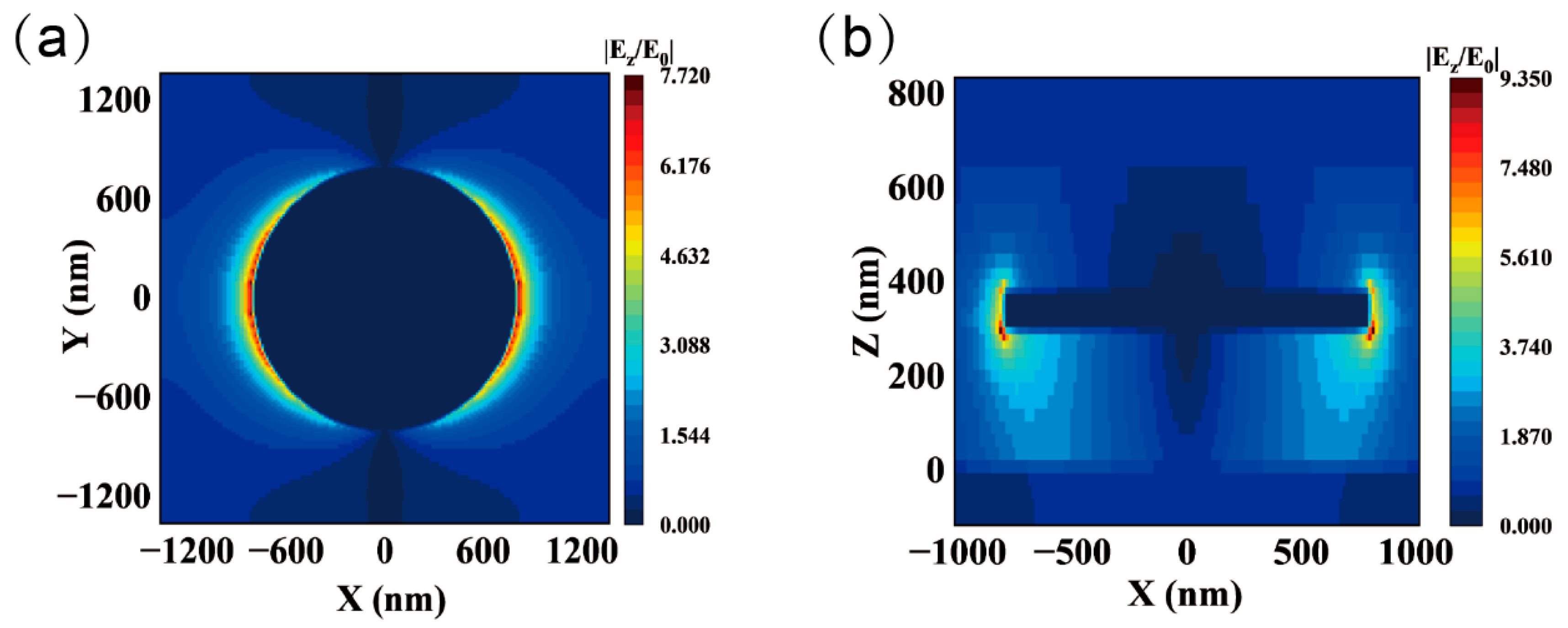
For a disk diameter of 1.6 μm, a periodicity of 2.5 μm, and a thickness of 70 nm with Au as the material, the plasmonic resonance peak occurs at a wavelength of 4 μm. The simulated electric field distribution (
Figure 4a,b) shows that the field intensity reaches a peak value of approximately
, highly localized around the edges of the disks. This ring-shaped high-intensity region indicates the strong confinement of the optical field induced by LSPR. In contrast, the electric field intensity in the gap between adjacent disks is significantly reduced (
), suggesting that the resonance is primarily governed by individual disk elements, with negligible contribution from array coupling effects. Furthermore, the low optical loss of the SiO
2 substrate suppresses field leakage into the substrate, allowing for greater energy confinement at the disk edges. These observations confirm the metasurface’s precise control over infrared field localization through geometric parameter optimization.
The MoSe
2 film, synthesized in situ on a SiO
2 substrate via selenization process, was transferred onto the metasurface array to construct a metasurface-enhanced MoSe
2 photodetector, as illustrated in
Figure 5a,c, which presents the current–voltage (
I–V) characteristics of the device measured under dark conditions and under illumination at the target wavelength. The
I–V curves exhibit distinct photoresponse across various infrared wavelength bands, along with a well-defined linear relationship, indicating the formation of an ideal Ohmic contact between the electrodes and the photosensitive MoSe
2 layer. The formation of an Ohmic contact is critical to the performance of photodetectors. Under ideal Ohmic contact conditions, carrier injection and extraction between the metal electrodes and the semiconductor are not limited by energy barriers, allowing carriers to move freely under an applied electric field. This effectively eliminates the nonlinear rectification behavior typically caused by Schottky barriers. The linearity of the
I–V characteristics further confirms that the variations in current observed during measurements are purely due to changes in carrier concentration induced by light illumination.
Under illumination at various wavelengths, the device demonstrates significant photoresponse characteristics, with photocurrent enhancement observed across all wavelengths compared to dark conditions. This indicates that photon energy at 808 nm, 1064 nm, 1342 nm, 4 μm, 6 μm, and 10 μm can effectively excite photogenerated carriers, thereby improving the device’s conductivity. The photocurrent–time curves of this metasurface-enhanced photodetector exhibit a typical two-stage rising behavior under all tested wavelengths: an immediate rapid increase upon illumination onset, followed by a slow ascending phase lasting several seconds. This phenomenon suggests the photoresponse process involves multiple physical mechanisms, including transient separation of photogenerated carriers, trap-state release effects, Schottky barrier modulation, and thermal response effects. Additionally, under lower light intensities, the proportion of the slow-rising component in the total photocurrent decreases, indicating its light intensity-dependent contribution.
Upon illumination, photogenerated carriers are promptly injected into the MoSe2 and are rapidly separated and transported to the electrodes under the influence of an external bias, leading to a sharp rise in photocurrent. The plasmonic resonance effect of the metallic metasurface further enhances the local electric field, thereby improving the light absorption capability of the vdWs material and significantly increasing the photocarrier generation rate. In addition to optical field enhancement, the metasurface also plays a pivotal role in photocurrent transport through the formation of a Schottky junction between the metal and the MoSe2 thin film. Due to the presence of a Schottky barrier, a portion of carriers accumulates near the barrier region, resulting in a relatively high initial photocurrent. Nevertheless, the photocurrent does not reach a steady state immediately after illumination; instead, it enters a slow-rising phase and gradually stabilizes over several seconds. This slow increase is likely related to the release of trap states. A large number of trap states may exist within the MoSe2 thin film and at its interfaces, which can capture some of the photogenerated carriers and suppress further photocurrent growth. Under continuous illumination, these trapped carriers are gradually released over time through thermal activation or quantum tunneling, thereby increasing the free carrier concentration and sustaining the continued rise in photocurrent. During the initial illumination phase, a fraction of photogenerated carriers is confined by the Schottky barrier, preventing their immediate participation in conduction. However, as the illumination persists, modulations in the local electric field may lead to a reduction in the effective barrier height, enabling more carriers to overcome the barrier and contribute to conduction, which further enhances the photocurrent.
After the illumination is turned off, the photocurrent does not immediately return to the dark current level, but instead exhibits a noticeable hysteresis effect. This behavior may be primarily governed by the time scale associated with the release of trap states—that is, a portion of the photogenerated carriers remains trapped after the light is removed, and is gradually released over an extended period. Additionally, the slow recovery of the Schottky barrier may influence the decay dynamics of the photocurrent. On the other hand, the relaxation time of the thermal response is relatively long; the gradual decrease in local temperature can lead to a sustained generation of thermally excited carriers, further contributing to the delayed recovery of the photocurrent. These combined effects result in a prolonged decay period following the termination of illumination. To further investigate the photoresponse characteristics of the metasurface-enhanced photodetector under varying power conditions, the device’s I–t response was measured and analyzed under 4 μm wavelength illumination. The experimental results show that the photocurrent increases with increasing optical power, indicating that the device effectively converts optical signals into electrical signals. The experimental results indicate that the device exhibits a distinct photoresponse not only at 4 μm but also at 6 μm and 10 μm, suggesting that the enhancement effect induced by the metasurface is not confined to a single wavelength but extends across a broad spectral range. The simulated electric field distribution in
Figure S2 shows that there is also an obvious field enhancement at 6 μm and 10 μm. This phenomenon is likely attributed to the structural parameters of the metasurface, such as its periodicity, duty cycle, and metal thickness. In periodic metasurface structures, the distribution of plasmonic resonance modes can be influenced by the intrinsic properties of the materials, the angle of incidence, and the coupling mechanism of the optical field, thereby resulting in multiple regions of optical enhancement. Moreover, the excitation of higher-order resonance modes may further broaden the spectral range over which enhancement occurs, enabling significant absorption enhancement across a wide portion of the MIR region. This broadband enhancement characteristic greatly improves the practical utility of the photodetector, making it suitable for a wider range of MIR applications.
Under low optical power conditions, the device exhibits a high photoresponsivity and specific detection, reaching up to 7.1 mA/W and 1.12 × 10
8 Jones. Furthermore, as shown in
Figure S3 depicting the device’s 1/f noise power density spectrum, the knee frequency of the device’s
1/f noise is identified at 966 Hz. Below this knee frequency, the device noise is dominated by a combination of
1/f noise and
G–R noise. Above the knee frequency, the noise transitions to being predominantly white noise, which persists across all frequency bands. The device exhibits a noise current density of approximately 10
−21 A
2/Hz at high frequencies, where only white noise is present, resulting in low noise levels. Conversely, at low frequencies, the current density reaches 10
−19 A
2/Hz, primarily due to the cumulative effect of 1/f noise superposition [
23] (
Table 1).
However, as the incident power increases, the photoresponsivity gradually decreases. This behavior may be attributed to nonlinear recombination effects of photogenerated carriers at higher power levels [
29]. Under low-power illumination, the number of photogenerated carriers is relatively small, and the influence of trap-assisted carrier capture is weak, resulting in higher responsivity. In contrast, under high-power conditions, a larger population of photogenerated carriers may be excited, some of which undergo interband or non-radiative recombination processes, thereby reducing the overall photoresponsivity of the device. Moreover, the plasmonic enhancement effect provided by the metasurface may experience partial saturation or screening at elevated power levels. This could lead to a reduction in the local electric field enhancement, which, in turn, limits the rate of photocurrent increase under high optical power. Such power-dependent behavior underscores the importance of optimizing both the optical and electronic characteristics of the device for efficient operation across a wide range of illumination intensities. Besides excellent performance parameters, atmospheric stability is crucial for device operation. As shown in
Figure S4, the MoSe
2 device maintains its initial photoresponse at 4 μm under 12.98 mW/cm
2 illumination after two-month ambient storage, demonstrating exceptional operational stability.


