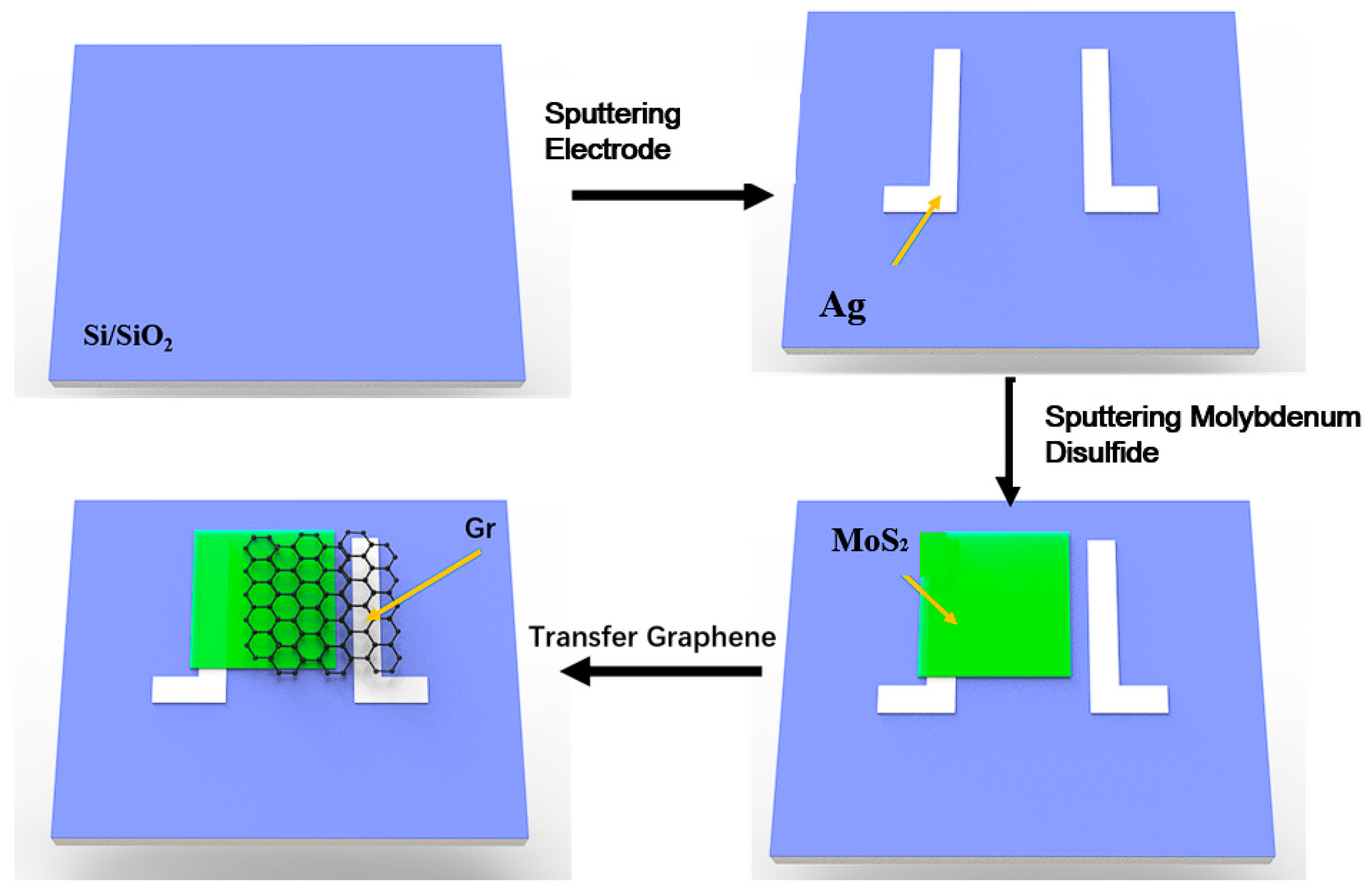
2. Materials and Methods
Figure 1 illustrates a schematic of a graphene/molybdenum disulfide (Gr/MoS
2) heterojunction photodetector. Initially, silicon (Si) substrates covered with approximately 300 nm of silicon dioxide (SiO
2) were cleaned by ultrasonic treatment in acetone and then rinsed with deionized water. Subsequently, the substrates were placed into an RF magnetron sputtering chamber, where patterned silver (Ag) electrodes were deposited using a mask and a high-purity (99.999%, General Research Institute for Nonferrous Metals) silver target. The sputtering power was set at 30 W, and the process lasted for 10 min. After that, patterned MoS
2 films were deposited by the mask using a high-purity (99.99%, General Research Institute for Nonferrous Metals) MoS
2 target. The background vacuum during magnetron sputtering was 9.6×10
−⁴ Pa, and the sputtering pressure was 2.5 Pa. To obtain high-quality MoS
2 films, experiments on MoS
2 films under different magnetron sputtering powers (60 W, 80 W, 100 W, and 120 W) were carried out.
Graphene (Gr) was grown on 0.025 mm-thick copper foil (99.8%, Thermo Scientific chemicals, Shanghai, China) by low-pressure chemical vapor deposition (CVD) at 1030 °C, using methane as the carbon source. The copper foils were first cleaned and then folded into a box shape before being placed into the CVD reaction chamber for graphene growth. To transfer the graphene from the copper foil to the substrate, a PMMA solution was spin-coated onto the graphene/copper sample and cured at 150 °C. The graphene/PMMA was then transferred to the substrate with Ag electrodes and MoS2 using a bubbling method. The sample was heated again to 120 °C to evaporate water and ensure a strong bond between the graphene and the substrate, followed by the removal of the PMMA using acetone. The photosensitive area of the device was 0.7 cm × 0.7 cm.
Finally, the physical and electrical properties of the materials and devices were tested using X-ray photoelectron spectroscopy (Thermo Scientific, Waltham, MA, USA, K-Alpha), Raman spectroscopy (HORIBA, Kyoto, Japan, HR-800), spectroscopic ellipsometry (VASE, M-2000D Spectroscopic Ellipsometer, J. A. Woollam, Shanghai, China), and a customized photovoltaic testing system (comprising a Keithley 2600 source meter, a probe station, and a laser source with a wavelength range of 400–650 nm).
3. Results and Discussion
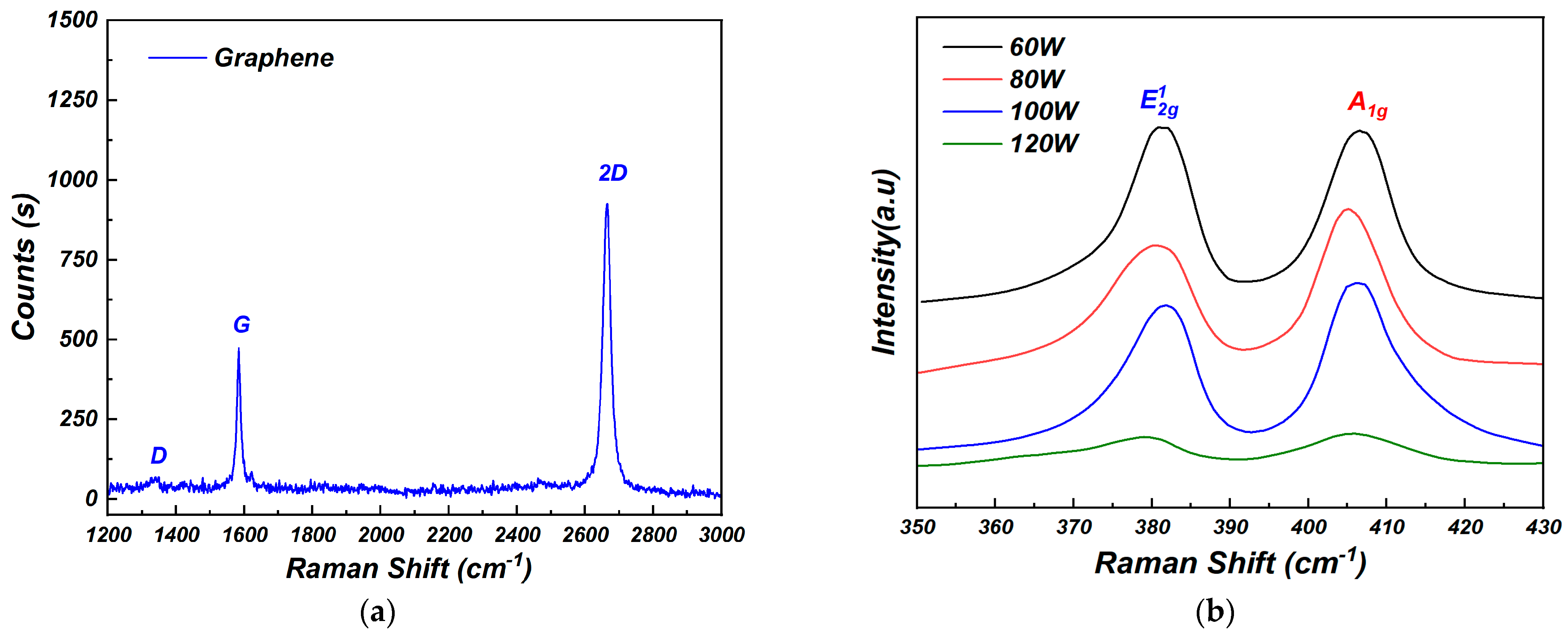
In order to characterize the properties of graphene film, Raman spectroscopy was performed and the results are shown in
Figure 2a. The laser wavelength was 532 nm and the power was 100 mW. As shown in
Figure 2a, two distinct peaks appeared in the Raman spectrum. They were located at 1587 cm
−1 and 2682 cm
−1, which corresponded to the G and 2D peaks of graphene, respectively [
14]. Almost no peak was observed at 1350 cm
−1, indicating that the graphene had a negligible level of defects and good quality [
14]. Using the peak intensities of G and 2D, I
2D/I
G > 2 could be obtained. The results indicate that the graphene obtained by the CVD method was a high-quality monolayer structure.
To find out the RF magnetron sputtering process effects on the properties of molybdenum disulfide films, different sputtering powers (60 W, 80 W, 100 W, and 120 W) under 15 min sputtering time were studied. Raman spectroscopy measurements were used to analyze the prepared films, as shown in
Figure 2b. The incident laser was selected as 532 nm and the laser power was 100 mW. As shown in
Figure 2b, two obvious diffraction peaks appeared in Raman spectra of the molybdenum disulfide prepared at different sputtering powers. These two diffraction peaks corresponded to the Mo-S bond perpendicular to the interlayer-direction out-of-plane relative vibration mode
and the Mo-S bond along the in-plane relative vibration mode A
1g [
15], which are the Raman characteristic diffraction peaks of 2H-MoS
2. When the sputtering power increased from 60 W to 120 W, the peak intensity of A
1g and
increased. This may be attributed to the molybdenum and sulfur atoms not being fully excited to the substrate surface under the low-sputtering-power condition [
16]. High sputtering power resulted in the incomplete combination reaction of molybdenum and sulfur atoms, which led to the degradation of the film. Meanwhile, the distance between the diffraction peaks of
and A
1g decreased, especially when the sputtering power reached 100 W. The results indicate that choosing the sputtering power of 100 W was beneficial to obtain high-quality molybdenum disulfide film. For the 100 W-sputtering-power sample,
and A
1g was located at 382.8 cm
−1 and 409.5 cm
−1, respectively. The difference between these two peaks was 26.7 cm
−1, which indicated that the MoS
2 film was between five and seven layers [
17].
The properties of molybdenum disulfide film deposited at 100 W sputtering power was further analyzed by the XPS, as shown in
Figure 3. All spectra were calibrated with a C
1s peak of 284.8 eV to eliminate the charge effect. As shown in
Figure 3a, except for the elemental peaks introduced by the substrate, the main peaks were attributed to Mo and S. When the sputtering power increased from 80 W to 100 W, the ratio of Mo atoms decreased from 44.73 a.t.% to 40.69 a.t.% and the ratio of S atoms increased from 55.27 a.t.% to 59.31 a.t.%. The value of Mo/S changed from 1/1.23 to 1/1.45, which was closer to the standard stoichiometric ratio of 1/2. This indicates that the molybdenum disulfide prepared by magnetron sputtering was composed of molybdenum-rich sulfur deficiency, which is consistent with the results of molybdenum disulfide prepared by magnetron sputtering reported in the literature [
16]. Compared to the molybdenum disulfide film deposited at 80 W sputtering power, the stoichiometric ratios of Mo and S atoms were closer to the ideal values. This may be attributed to the fact that higher sputtering power could make the Mo and S atoms be in higher excited states with higher reactivity, which was beneficial for reaction and bonding.
Figure 3b shows the XPS peak fitting results of Mo
3d and S
2s. The results indicate that Mo
3d was a typical double-peak, and its binding energies were located at 228.5 eV, 229.4 eV, 231.9 eV, and 233.3 eV, respectively [
16]. The Mo
6+3d peak was not found, indicating that the molybdenum disulfide film had no oxidation [
18]. The Mo
3d peaks at low binding energy belonged to Mo
4+ in metallic 1T-MoS
2, while the peaks at high binding energy belonged to Mo
4+ in semiconducting 2H-MoS
2 [
16]. When the sputtering power was increased from 80 W to 100 W, an increase in the component of Mo
3d in 2H-MoS
2 could be obtained from the area of the fitting peaks. All results indicate that molybdenum disulfide sputtered at a sputtering power of 100 W showed a suitable Mo/S ratio and more components of the semiconductor phase.
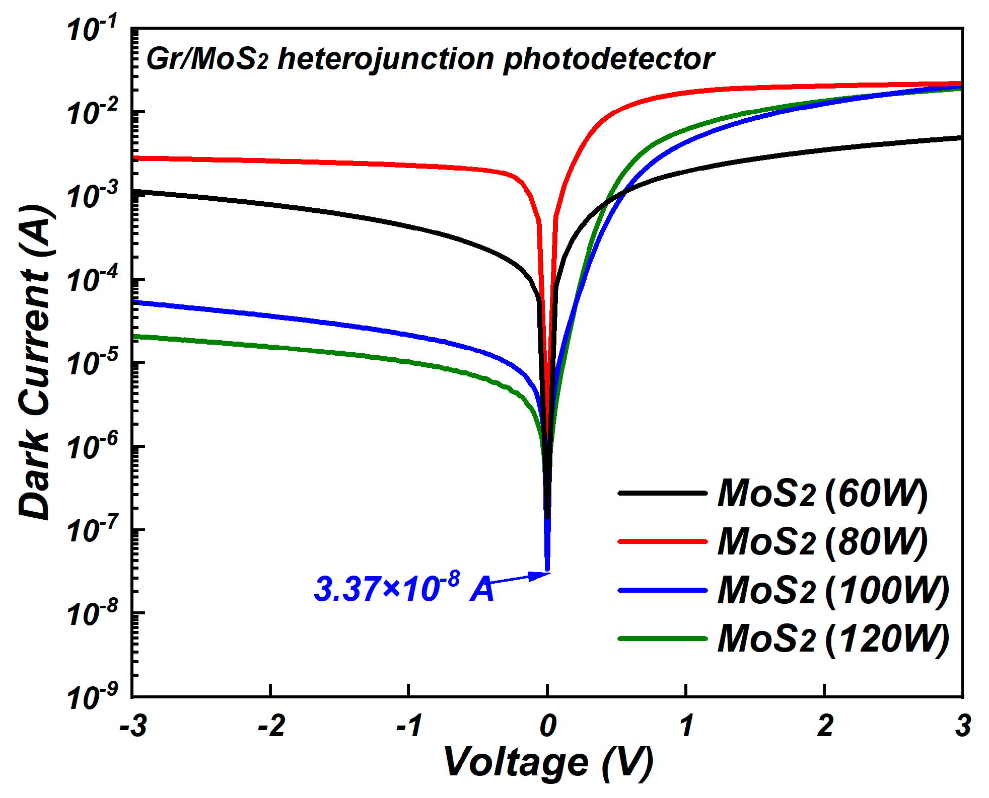
To evaluate the dark current of the graphene/molybdenum disulfide heterojunction, the graphene/molybdenum disulfide heterojunction photodetectors were produced and the I–V measurements were tested under dark conditions. As shown in
Figure 4, except for the molybdenum disulfide at a sputtering power of 80 W, the dark current of the graphene/molybdenum disulfide heterojunction photodetectors exhibited a decreasing trend as the sputtering power increased from 60 W to 120 W. At a bias voltage of 0 V, the dark current of graphene/molybdenum disulfide heterojunction photodetectors prepared at the sputtering powers of 60 W, 80 W, 100 W, and 120 W was 1.14 × 10
−7 A, 1.33 × 10
−6 A, 3.37 × 10
−8 A, and 1.08 × 10
−7 A, respectively. The dark current reached a minimum value of 3.37 × 10
−8 A for molybdenum disulfide at a sputtering power of 100 W. This is comparable with the dark current value of photodetectors based on mechanically exfoliated MoS
2 on graphene [
18]. Furthermore, it is an order of magnitude lower than the dark current value of ~10
−7 A for graphene/Si photodetectors [
19]. The results indicate that using the magnetron-sputtered molybdenum disulfide to form the graphene/molybdenum disulfide heterojunction could decrease the dark current of the graphene photodetectors based on the advantages of large area and low cost.
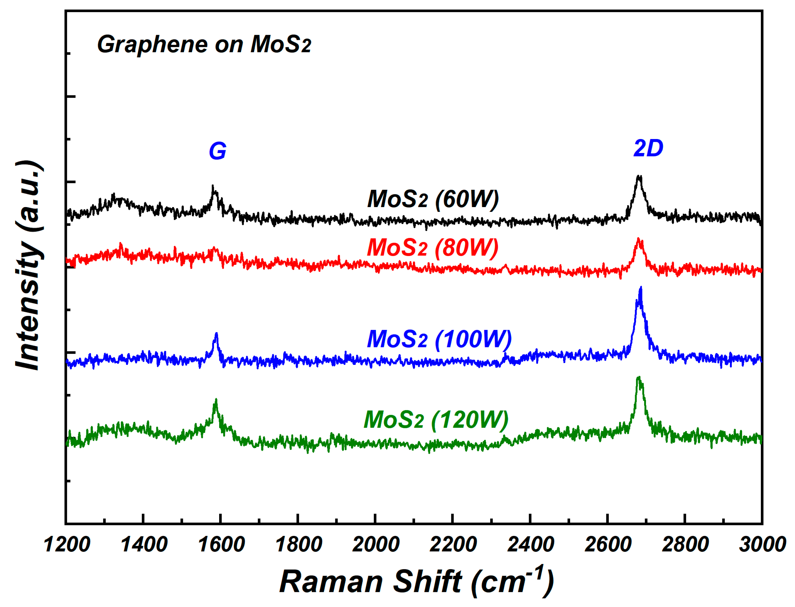
In order to find out the changes in dark current, the Raman spectra of graphene on MoS
2 were measured and the results are shown in
Figure 5. The G peak and 2D peak could be found in the Raman spectra of graphene on MoS
2 with different sputtering conditions. The presence of G and 2D peaks prove the existence of graphene on MoS
2. For molybdenum disulfide sputtered at a sputtering power of 80 W, the weak response of G peak was observed compared with in other sputtering conditions. The G-band represents the planar configuration
sp2 bonded carbon that constitutes graphene and it is very sensitive to the effects of stress. The decrease in the G peak may have been caused by the adsorption of atoms on graphene surfaces disrupted the symmetry of the graphene’s stacking structure [
14]. The degradation of graphene occurred when the graphene was transferred to molybdenum disulfide substrate sputtered at a sputtering power of 80 W, leading to the largest dark current for molybdenum disulfide at a sputtering power of 80 W in
Figure 4.
The Schottky barrier height values of graphene/molybdenum disulfide heterojunction photodetectors were calculated using the following formulas [
20,
21]:
where
represents the Schottky barrier height,
Aeff is the effective working area of the photodetector,
A* is the Richardson constant (0.70 × 10
−6 A cm
−2 K
−2 for MoS
2),
Is is the reverse saturation current,
q is the elementary charge with a value of 1.602 × 10
−19 C, K is the Boltzmann constant (1.38 × 10
−23 J/K), T is the absolute temperature, and
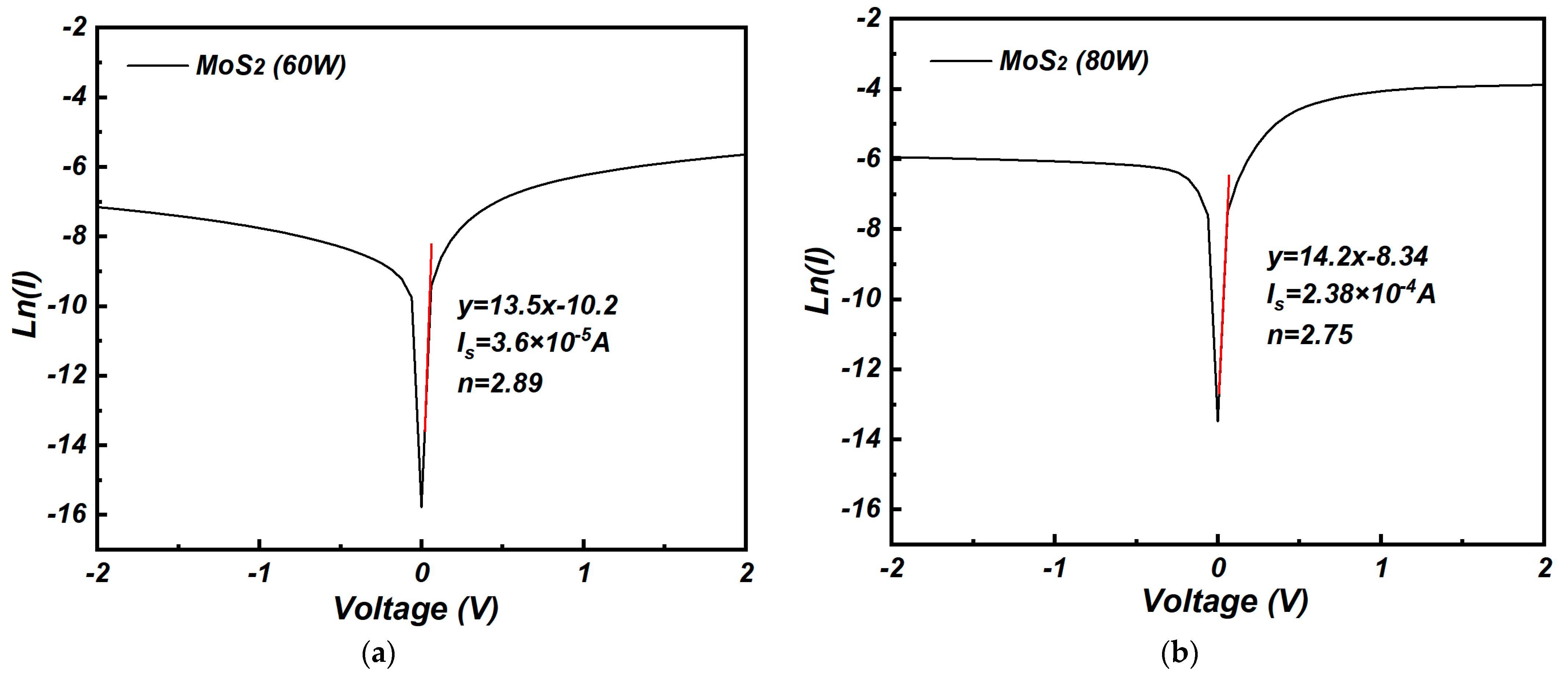
n is the ideal factor of the device. The fitting results of I-V curves in
Figure 4 are shown in
Figure 6.
As shown in
Table 1, the Schottky barrier height (
) of the graphene/molybdenum disulfide heterojunction prepared at the sputtering powers of 60 W, 80 W, 100 W, and 120 W was 0.644 eV, 0.596 eV, 0.739 eV, and 0.721 eV, respectively. For molybdenum disulfide at a sputtering power of 100 W, the Schottky barrier height of the graphene/molybdenum disulfide heterojunction reached maximum value of 0.739 eV. A higher Schottky barrier height was beneficial to decrease the transportation of carriers to form the dark current. Meanwhile, the ideal factor was calculated to be 2.3. According to PN junction theory, when the ideal factor approaches or equals 2, it indicates that the current transport mechanism within the device has shifted from diffusion current to recombination current [
22]. The excessive recombination current was attributed to a high density of defects at the interface, which increased carrier recombination. This may have been related to defects present on the surface of the fabricated graphene and the numerous dangling bonds on the sputtered MoS
2 surface, leading to significant recombination current at the interface.
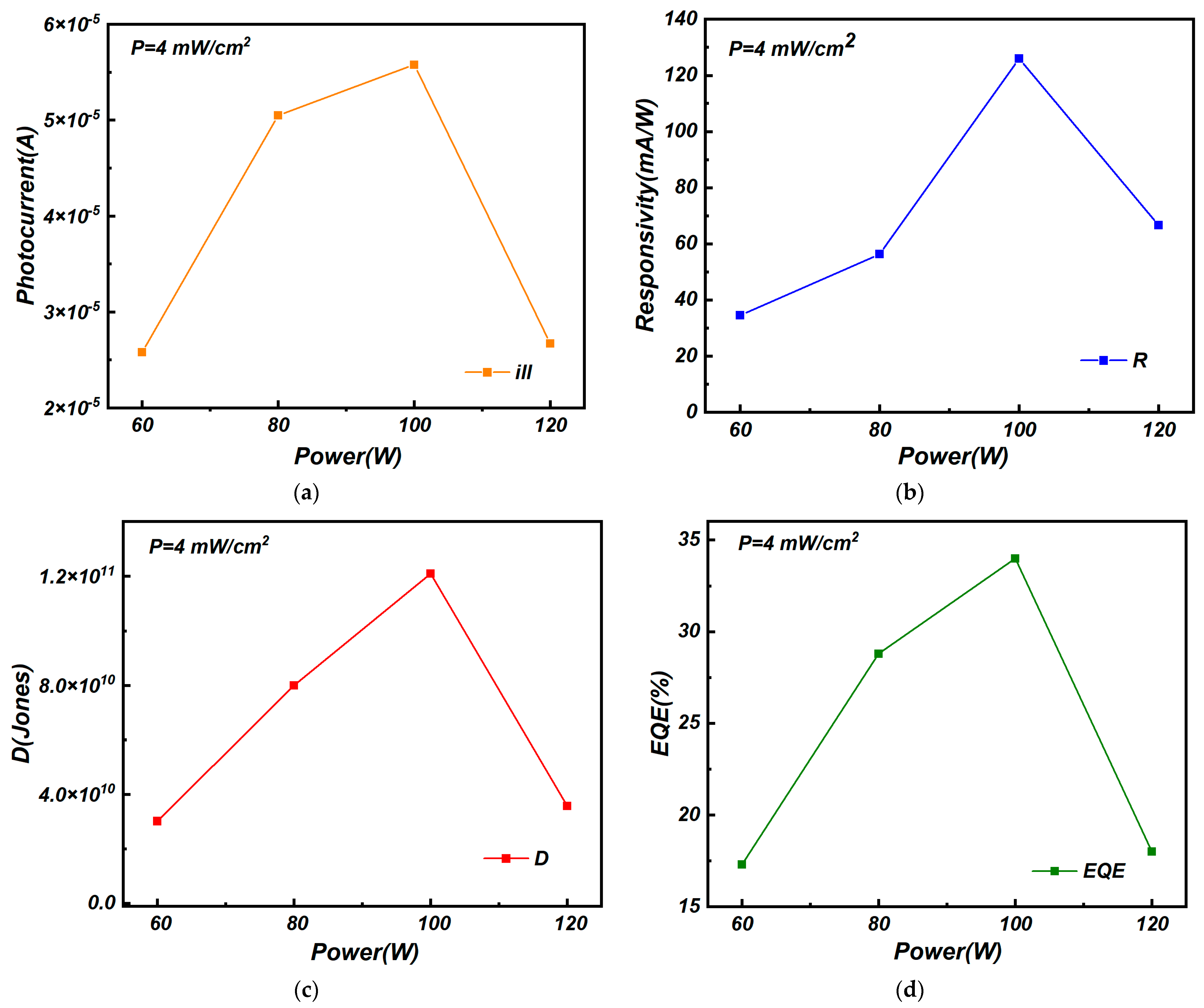
To further evaluate the performances of the graphene/molybdenum disulfide heterojunction photodetectors under illumination conditions, I-V measurements were carried out and the calculated parameters of the graphene/MoS
2 heterojunction photodetectors are shown in
Figure 7. For illumination conditions, an incident light wavelength of 460 nm with an incident power of 4 mW/cm
2 was used. As shown in
Figure 7a, the photocurrent of graphene/molybdenum disulfide photodetectors increased firstly as the sputtering power increased from 60 W to 100 W and then decreased. At the sputtering power of 100 W, the photocurrent of the graphene/molybdenum disulfide photodetector reached the maximum value of 5.58 × 10
−5 A. The main reason for this phenomenon was that the molybdenum and sulfur atoms could not be fully excited to the substrate surface in the low-sputtering-power condition, while high sputtering power resulted in the incomplete combination reaction of molybdenum and sulfur atoms.
As shown in
Figure 7b, the responsivity of the graphene/molybdenum disulfide photodetectors also changed with the sputtering power. It was consistent with the variation in the photocurrent. For molybdenum disulfide in the 100 W-sputtering-power condition, the responsivity of the graphene/molybdenum disulfide photodetector reached the maximum value of 126 mA/W. Meanwhile, the measured detectivity values of the graphene/molybdenum disulfide photodetectors, shown in
Figure 7c, and the quantum efficiency, shown in
Figure 7d, were 1.21 × 10
11 Jones and 34%, respectively. They also reached maximum values under the 100 W-sputtering-power condition. The results suggest that, owing to the reduction in dark current and high quality of molybdenum disulfide in the 100 W-sputtering-power condition, the graphene/molybdenum disulfide photodetector could achieve the best photodetection properties.
In addition, the Ag electrode-and-graphene and Ag electrode-and-molybdenum disulfide contact characteristics were also studied. The current–voltage result of the Ag electrode-and-graphene contact is shown in
Figure 8a. The linear relationship observed in the curves indicates that the Ag electrodes formed ohmic contact with the graphene, rather than Schottky contact. In
Figure 8b, the contact of the Ag electrode and molybdenum disulfide shows a linear-like trend with a contact resistance of approximately 368 mΩ. This may be attributed to the amount of sulfur vacancies in the molybdenum disulfide, which could successfully dope the contact regions by introducing sulfur vacancies [
23].
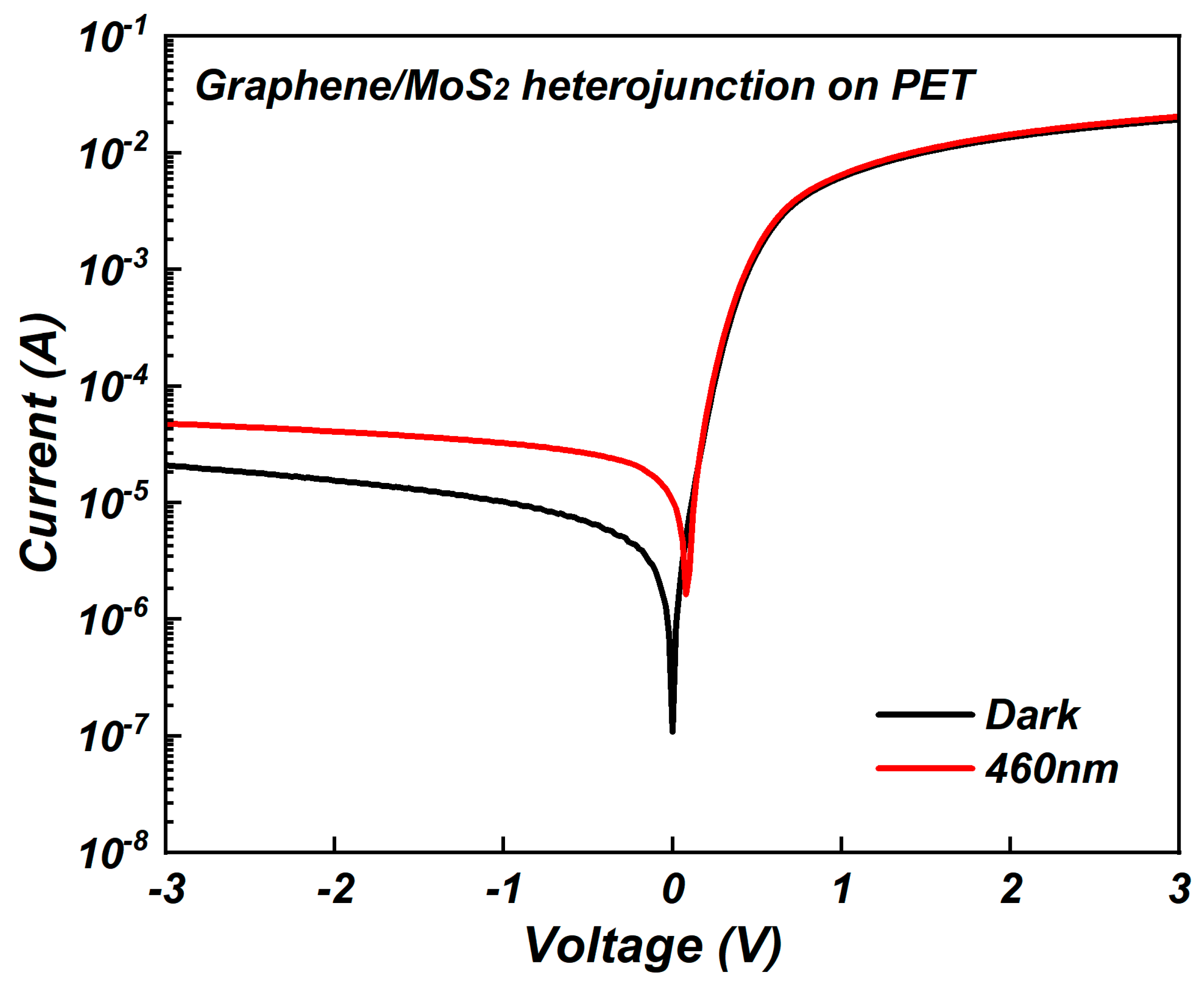
The application of graphene/molybdenum disulfide heterojunctions in flexible photodetectors were also investigated. Molybdenum disulfide was deposited on polyethylene terephthalate (PET) substrate using a sputtering power of 100 W to construct the graphene/molybdenum disulfide heterojunction. The schematic of the graphene/molybdenum disulfide heterojunction on PET is the same as that in
Figure 1. Under illumination, incident light with a wavelength of 460 nm and a power of 4 mW/cm
2 was used. The I–V results are shown in
Figure 9. At a bias voltage of 0 V, the dark current of the graphene/molybdenum disulfide heterojunction photodetector was 6.54 × 10
−5 A, which was higher than the dark current of 3.37 × 10
−8 A on silicon dioxide substrate under the same conditions. This may have been due to the flexible nature of PET leading to more defects within the material, increasing carrier recombination and thus raising the dark current. At a bias voltage of 0 V, when the incident light wavelength was 460 nm, the net current, responsivity, and detectivity of the graphene/molybdenum disulfide heterojunction photodetector on the flexible PET substrate were 2.53 × 10
−5 A, 6.32 mA/W, and 2.85 × 10
9 Jones, respectively. Despite the higher dark current on the PET substrate, the response photocurrent under illumination still indicates the potential application of this heterojunction in flexible photodetectors.
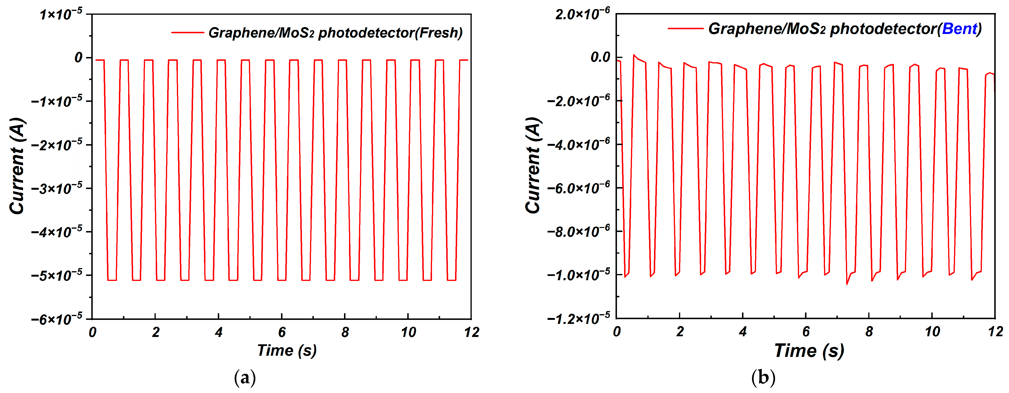
The stability of graphene/molybdenum disulfide photodetectors on flexible PET substrates was also assessed. An I–T test was carried out to evaluate whether the graphene/molybdenum disulfide heterojunction photodetectors on PET substrate could work stably after bending 30° and 50 times, as shown in
Figure 10. The graphene/molybdenum disulfide photodetectors on flexible PET substrate showed good stability when the device was not bent. After bending 30° and 50 times, graphene/molybdenum disulfide photodetectors on flexible PET substrate also showed stability, although the light response showed negligible variation after bending. This may have been caused by the change in the microstructure in the material due to frequent bending, which may have caused fatigue effects and reduced the performance of the material.


