Abstract
Dynamic random-access memory (DRAM) is a vital component in modern computing systems. Enhancing memory performance requires maximizing capacitor capacitance within DRAM cells, which is achieved using high-k dielectric materials deposited as thin, uniform films via atomic layer deposition (ALD). Precise film deposition that minimizes electronic defects caused by charged vacancies is essential for reducing leakage current and ensuring high dielectric strength. In this study, we fabricated metal–insulator–metal (MIM) capacitors in high-aspect-ratio trench structures using remote plasma ALD (RP-ALD) and direct plasma ALD (DP-ALD). The trenches, etched into silicon, featured a 7:1 aspect ratio, 76 nm pitch, and 38 nm critical dimension. We evaluated the electrical characteristics of HfO2-based capacitors with TiN top and bottom electrodes, focusing on leakage current density and equivalent oxide thickness. Capacitance–voltage analysis and X-ray photoelectron spectroscopy (XPS) revealed that RP-ALD effectively suppressed plasma-induced damage, reducing defect density and leakage current. While DP-ALD offered excellent film properties, it suffered from degraded lateral uniformity due to direct plasma exposure. Given its superior lateral uniformity, lower leakage, and defect suppression, RP-ALD shows strong potential for improving DRAM capacitor performance and serves as a promising alternative to the currently adopted thermal ALD process.
1. Introduction
Dynamic random-access memory (DRAM) is a widely used semiconductor device that serves as the main memory in computers. With the rapid increase in mobile device usage and exponential improvements in CPU performance, DRAM has continuously evolved to meet higher performance demands [1,2,3]. Each DRAM cell, the smallest memory unit, consists of a transistor acting as a switch and a capacitor that stores electric charge. Unlike flash memory, which uses a floating gate to store charges beneath the gate electrode and retain data without a power supply, DRAM relies on separately fabricated capacitors to store charges [4,5,6,7]. As DRAM loses stored information due to charge leakage when reading data from the capacitor, a refresh operation is required to periodically replenish the charge [8,9].
To increase chip yield per wafer and enhance the speed of semiconductor devices, DRAM must undergo continuous process miniaturization, and extending the refresh cycle is essential for improving performance. As a result, new materials and advanced process technologies are being actively developed to maintain high dielectric capacitance [10,11,12]. A central approach to DRAM miniaturization is increasing the dielectric capacitance of capacitors, which is achieved by fabricating high-aspect-ratio trench structures and depositing dielectric films uniformly. In capacitor fabrication, trenches with aspect ratios exceeding 100:1 are formed and arranged laterally to increase integration density [13,14,15]. However, this lateral configuration introduces thickness non-uniformity perpendicular to the deposition direction. To ensure reliable DRAM performance, uniformity of less than 5% between the top and bottom of the trench is required, significantly complicating the process [16].
To maintain sufficient dielectric thickness while achieving an equivalent oxide thickness (Tox) below 1 nm and minimizing leakage current, various high-k materials are being explored [17,18,19]. Uniform deposition processes that ensure the high quality of these high-k materials are becoming increasingly important. Currently, ZrO2/Al2O3/ZrO2 (ZAZ) composite films are widely used as dielectric materials in DRAM capacitors, but miniaturization imposes physical constraints that ultimately reduce their charge storage capability [20,21,22]. Achieving sufficient capacitance and suppressing charge loss requires a combination of high-k materials and low leakage current density (J). In this regard, materials such as HfO2, ZrO2, TiO2, Al-doped TiO2, and SrTiO3 have been extensively studied as potential alternatives to the current ZAZ dielectric films. While high-k materials offer improved electrical performance, such as reduced leakage current at low effective oxide thickness (tox), their low band offset with metal electrodes—due to small bandgaps—often necessitates relatively great physical thickness. Additionally, both the choice of deposited material and the deposition process are critical to achieving high capacitance and low leakage current [23,24].
Historically, planar semiconductor devices were able to achieve high-quality thin films using chemical vapor deposition [25,26]. However, as miniaturization has progressed toward three-dimensional structures, such as FinFETs, gate-all-around structures, and trenches, atomic layer deposition (ALD), offering near-perfect step coverage, has become the standard [27,28]. Currently, ALD is widely adopted in semiconductor deposition processes as the optimal technique for achieving uniform thin films on memory devices with trench structures and nanometer-scale thicknesses. ALD operates by depositing one atomic layer at a time, followed by purging and reaction steps, enabling excellent step coverage and uniformity, though its inherently slow deposition rate remains a persistent challenge [29,30].
ALD processes are categorized into thermal ALD and plasma-enhanced (PE) ALD based on how reactive gases are activated. PE-ALD is favored in many semiconductor applications due to its lower process temperature, denser films, and higher deposition rate. Nonetheless, for DRAM capacitors, which use laterally aligned trenches, thermal ALD remains the preferred method despite its lower deposition rate. PE-ALD can be further divided into direct plasma (DP) ALD and remote plasma (RP) ALD. In DP-ALD, plasma is generated directly inside the reaction chamber, energizing gases in situ. While DP-ALD offers high deposition rates and excellent film quality, it can lead to ion bombardment of the substrate or film surface, resulting in interface damage and degradation of film properties [31,32,33]. As DRAM structures evolve into horizontally stacked trench arrays with hundreds of layers, the strong directionality of radicals in DP-ALD, which are guided by the electric field, introduces challenges for uniform film formation. As a result, thermal ALD remains the dominant method for capacitor fabrication. However, for future extreme miniaturization and higher productivity, the implementation of PE-ALD is becoming essential. RP-ALD, which isolates the plasma generation from the process chamber and delivers only activated radicals, has emerged as a promising alternative for mitigating plasma-induced damage and electric-field directionality issues observed in DP-ALD. Nevertheless, due to the limited lifetime of radicals in RP-ALD, the optimization of equipment design and process parameters is necessary, and further research is required to obtain films with the desired properties [34,35].
Despite the widespread use of ALD techniques in DRAM fabrication, there remains a lack of direct comparative analysis between DP-ALD and RP-ALD, specifically for high-aspect-ratio trench structures. Therefore, this study investigates the differences between these plasma-based ALD techniques for trench structures. Hafnium oxide, a representative high-k material, was deposited using both DP-ALD and RP-ALD to examine the impact of plasma on deposition characteristics. Trenches with a 76 nm pitch, 38 nm critical dimension (CD), and an aspect ratio of 7:1 were fabricated, and the resulting deposition profiles were analyzed using scanning electron microscopy (SEM) [36,37,38]. To assess film uniformity, depositions were also performed on 6-inch wafers and evaluated using ellipsometry. Additionally, plasma-induced defects such as oxygen vacancies were investigated. Thin films obtained from the RP-ALD and DP-ALD processes were characterized via X-ray photoelectron spectroscopy (XPS), and their electrical properties, such as dielectric constant and leakage current, were evaluated. Based on leakage current analysis, RP-ALD demonstrated superior performance compared to DP-ALD. Step coverage was also found to be more favorable in RP-ALD than in DP-ALD. However, DP-ALD yielded higher dielectric constant values than RP-ALD, which can be attributed to the presence of oxygen vacancies in the HfO2 films. The excellent lateral uniformity and superior thin-film properties observed in RP-ALD suggest that it may serve as a viable replacement for thermal ALD in DRAM capacitor fabrication, potentially enhancing device performance [39,40,41,42,43,44].
2. Materials and Methods
2.1. Deposition of HfO2 Thin Films Using RP-ALD and DP-ALD
Figure 1 shows the silicon trench structure and the process conditions used for the deposition tests. In Figure 1a, a silicon substrate with trenches having an aspect ratio of 7:1, a pitch of 76 nm, and a CD of 38 nm was fabricated and used to evaluate both lateral and vertical deposition using DP-ALD. Figure 1b shows a corresponding setup for deposition using RP-ALD on a similarly structured substrate. These trench structures were fabricated using a test pattern wafer (SK Hynix Inc., Icheon-si, Republic of Korea). Film uniformity was evaluated using an ellipsometer (Elli-SE-U, Ellipso Technology, Daejeon, Republic of Korea) after deposition via both the DP and RP methods.
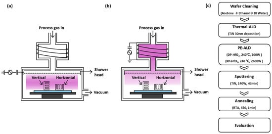
Figure 1.
Deposition processes and conditions for laterally and vertically aligned trench-structured substrates simulating DRAM capacitors. (a) DP-ALD process. (b) RP-ALD process. (c) Process flow for HfO2 deposition using DP-ALD and RP-ALD.
Figure 1c outlines the detailed process flows for the DP and RP deposition methods. In DP-ALD, plasma was generated directly inside the PE-ALD chamber, where reactive gases such as O2 were introduced near the substrate, and a plasma power of 200 W was applied. By contrast, RP-ALD used a remote plasma source (En2ra-RPS, EN2CORE Technology, Daejeon, Republic of Korea), where only radicals activated in a remote plasma zone were introduced into the chamber. To generate a sufficient radical density, approximately 2600 W of remote plasma power was used, and the radicals were delivered to the chamber using Ar as the carrier gas. For the deposition of the high-k dielectric layer, tetrakis(ethylmethylamido)hafnium (TEMA-Hf, iChems, Gyeonggi-do, Republic of Korea) was used as the precursor for HfO2 deposition. For electrical property evaluation, a 50 nm thick TiN bottom electrode was first deposited on the trench-structured substrate. HfO2 films were then deposited, followed by the formation of top TiN electrodes (200 μm in diameter, 50 nm in thickness) via a lift-off process. The TiN top electrodes were deposited by RF magnetron sputtering at room temperature for 43 min. To minimize defect density within the dielectric films, rapid thermal annealing was performed at 450 °C for 1 min in a nitrogen ambient atmosphere.
2.2. Evaluation of the Properties of Trenches Deposited by DP and RP-ALD
The HfO2 film thickness was measured using spectroscopic ellipsometry. To assess the uniformity of the DP and RP deposition processes, films were deposited on a 6-inch wafer, and thickness distributions were measured across the substrate, including along the X- and Y-axes, to further confirm the uniformity. The MIM capacitor thin film structure was analyzed using SEM (Nova NanoSEM 450, FEI, Hillsboro, OR, USA) at an accelerating voltage of 10 kV. Film composition and defects in the HfO2 films deposited by the DP and RP methods were analyzed and compared using XPS (NEXSA, Thermo Fisher Scientific, Seoul, Republic of Korea). XPS data were collected using an Escalab 250 photoelectron spectrometer (ThermoFisher Scientific, Waltham, MA, USA) using 300 W Al Kα irradiation. Furthermore, the dielectric capacitance and leakage current of the MIM capacitor were measured using a semiconductor characterization system (4200A-SCS, Keithley, Cleveland, OH, USA) connected to a microprobe station (APX-6B, WIT Co., Suwon, Republic of Korea). C–V measurements were conducted at 1 MHz.
3. Results
3.1. Characteristics of HfO2 Thin Films Deposited by DP-ALD and RP-ALD
Figure 2 illustrates the application of DP-ALD and RP-ALD processes for the deposition of hafnium oxide (HfO2) thin films on trench-structured substrates. The trenches had a depth of 600 nm, a pattern pitch of 76 nm, and a CD of approximately 38 nm, etched in a bar-type pattern. As shown in Figure 1, the patterns were arranged in both vertical and horizontal orientations, and the ALD processes were conducted using different types of plasma.
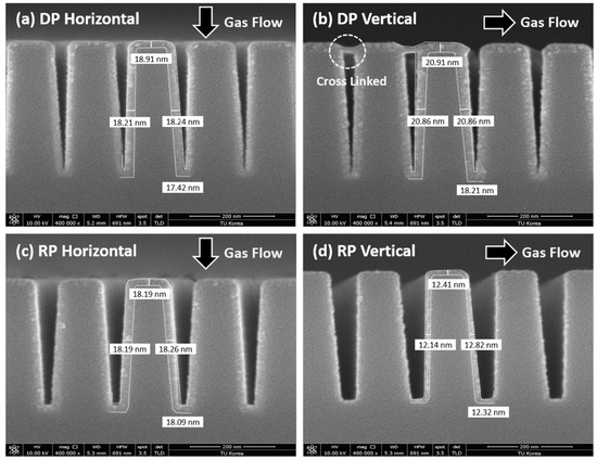
Figure 2.
Cross-sectional images of trenches deposited by DP-ALD: (a) horizontal deposition; (b) vertical deposition. Cross-sectional images of trenches deposited by RP-ALD: (c) horizontal deposition; (d) vertical deposition.
The deposition results using DP-ALD and RP-ALD are shown in Figure 2a,b and Figure 2c,d, respectively. For DP-ALD, horizontal deposition (Figure 2a) exhibited high step coverage owing to the perpendicular alignment between the deposition direction and the substrate orientation. By contrast, vertical deposition (Figure 2b) showed lower step coverage because the deposition direction was parallel to the trench orientation, limiting precursor penetration into the trench. In horizontal deposition, the upper and lower film thicknesses were approximately 18.9 and 17.4 nm, respectively, resulting in a step coverage of 0.92. For vertical deposition, the upper thickness was 20.9 nm and the lower was 18.2 nm, yielding a reduced step coverage of approximately 0.87. By contrast, RP-ALD achieved uniform HfO2 thin film deposition within the trench regardless of the substrate orientation. In horizontal deposition (Figure 2c), the airflow was perpendicular to the trench, allowing for uniform coating. Even in vertical deposition (Figure 2d), where the deposition direction was parallel to the trench, RP-ALD maintained conformal coverage deep into the trench, unlike DP-ALD.
Figure 3 summarizes the step coverage of the ALD processes based on the type of plasma used. For DP-ALD, the step coverage was 92.6% for horizontal deposition and 87.3% for vertical deposition. By contrast, RP-ALD achieved nearly 100% step coverage in both orientations, demonstrating superior deposition uniformity compared to DP-ALD. Regarding deposition rate, DP-ALD exhibited higher productivity, with rates of 0.97 Å/cycle and 1.12 Å/cycle for horizontal and vertical deposition, respectively. In comparison, RP-ALD showed relatively low deposition rates of 0.72 Å/cycle for horizontal deposition and 0.55 Å/cycle for vertical deposition. This difference can be attributed to the higher plasma energy delivered to the substrate in the DP-ALD process, which enhances deposition efficiency. Therefore, while DP-ALD is advantageous in terms of productivity, RP-ALD provides better performance in deposition uniformity.
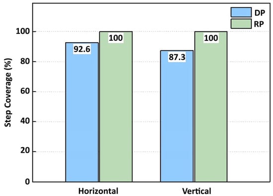
Figure 3.
Step coverage results for thin films deposited by DP-ALD and RP-ALD depending on the substrate orientation in the trench structure.
Figure 4 presents the thickness distribution of HfO2 thin films deposited on 6-inch (152 mm) wafers using DP-ALD and RP-ALD. In DP-ALD, a capacitively coupled plasma system based on RF power is used, resulting in noticeable film thickness non-uniformities, particularly in the central region of the wafer, owing to plasma influence. This variation appears as blue regions, indicating thinner films where plasma effects are stronger, and red regions, indicating thicker films where plasma influence is weaker, producing a distinct thickness gradient across the wafer. By contrast, RP-ALD utilizes an inductively coupled plasma system, where plasma is generated externally, and Ar+ ion emission is effectively blocked. Only reactive radicals are introduced into the chamber via the carrier gas, Ar. This configuration prevents ion-induced damage, such as that caused by Ar+ ions, thereby enabling uniform thin film deposition. The thickness variations observed in RP-ALD can be attributed to airflow distribution within the chamber rather than plasma-related effects.
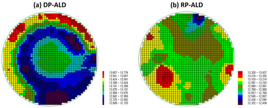
Figure 4.
Thickness uniformity measurement results for thin films on a 6-inch (152 mm) wafer based on the deposition type: (a) DP-ALD, (b) RP-ALD.
Figure 5 shows the thickness distribution of the HfO2 thin films, ranging from 12 to 13 nm depending on the type of plasma used. Non-uniformity, defined as (Maximum − Minimum)/(2 × Average), was approximately 5% for DP and 3% for RP. As shown in Figure 5a, the DP case exhibits a symmetric, bowl-shaped thickness profile centered on the wafer, which can be attributed to the influence of plasma. By contrast, the RP case in Figure 5b shows localized regions of thicker and thinner film, which appear to correlate with both the precursor injection position and the direction of gas exhaust. Thickness uniformity is a critical factor in plasma-enhanced ALD processes, as it directly impacts semiconductor device performance and manufacturing yield.
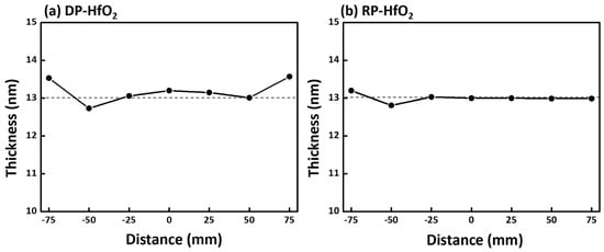
Figure 5.
Thickness distribution data for thin films deposited on a wafer: (a) DP-HfO2 and (b) RP-HfO2.
To investigate the defect density of the thin films based on plasma type, HfO2 films deposited by DP-ALD and RP-ALD were analyzed using X-ray photoelectron spectroscopy (XPS). Figure 6a,b show the XPS depth profile results, which assess elemental composition as a function of etching time. In both cases, the presence of C 1s within the films was negligible, suggesting that the detected surface carbon contamination originated from exposure during the FIB pre-treatment process, with minimal carbon content inside the films. This indicates that the deposition was conducted under optimal conditions. Figure 6c,d show the XPS spectra of Hf 4f for the films deposited by DP-ALD and RP-ALD, respectively. The intensity ratio between Hf 4 and Hf 4 was fixed at 3:4, and the peaks were deconvoluted into non-lattice Hfx+ and metallic Hf0 components. The proportion of non-lattice Hf was calculated to be 17.0% for DP-HfO2 and 13.6% for RP-HfO2, indicating a higher concentration of plasma-induced non-lattice Hf in the DP-HfO2 film. Similarly, Figure 6e,f present the deconvoluted O 1s spectra, separating lattice and non-lattice components corresponding to oxygen-related defects. The proportion of non-lattice oxygen was determined to be 9.82% for DP-HfO2 and 5.08% for RP-HfO2, confirming that the DP-HfO2 film contains a higher density of defects compared to the RP-HfO2 film.
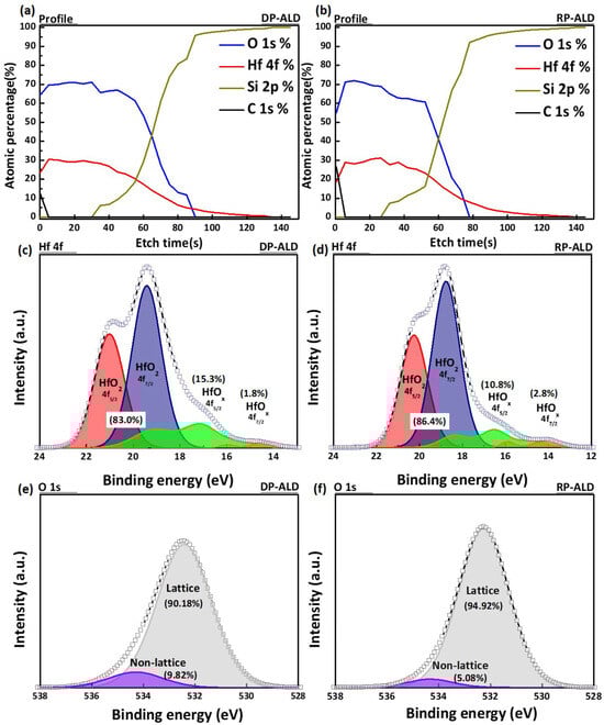
Figure 6.
XPS measurement data for HfO2 thin films fabricated via DP-ALD and RP-ALD: (a,b) depth profiling; (c,d) Hf 4f; (e,f) O 1s patterns.
3.2. MIM Device Electrical Characteristics
Figure 7 shows a comparison of the capacitance characteristics of DP-HfO2 and RP-HfO2 thin films with thicknesses ranging from 5 to 20 nm, measured at a frequency of 1 MHz. For dielectric films fabricated by both processes, C–V curves were obtained over a voltage sweep range of −2 V to +2 V, and all films exhibited typical and stable capacitance behavior throughout the measurement range. For 5 nm thick HfO2 films, the measured capacitance values were approximately 670 pF for DP-HfO2 and 620 pF for RP-HfO2. These results indicate that, under identical thickness and electrode area conditions, DP-HfO2 exhibits approximately 7.5% higher capacitance compared to RP-HfO2. Dielectric films exposed to plasma typically experience degradation in electrical properties owing to interfacial damage and increased leakage current. However, under certain conditions, plasma-induced damage has also been reported to enhance dielectric capacitance. In the case of HfO2 thin films deposited by plasma-assisted ALD, this anomalous behavior can be primarily attributed to the formation of oxygen vacancy (Vo) defects induced by ion bombardment from the plasma. Exposure to plasma can cause the dissociation of oxygen atoms at the HfO2 film surface or the metal–dielectric interface, increasing the concentration of oxygen vacancies. These defects act as donor-like charge states and generate localized electric dipoles within the dielectric layer. When subjected to an external electric field, these dipoles can reorient, enhancing dielectric polarization and increasing the overall dielectric permittivity. This behavior can be explained by the “defect–polarization model”, which suggests that changes in the dipole moment of oxygen vacancies contribute to an increase in the real component of permittivity, particularly under low-frequency electric fields. While a moderate level of plasma-induced defects may benefit dielectric capacitance enhancement, excessive defect generation can result in increased leakage current and compromised long-term reliability. Therefore, precise control over the concentration and spatial distribution of oxygen-related defects is essential for optimizing DRAM capacitor performance [45,46].
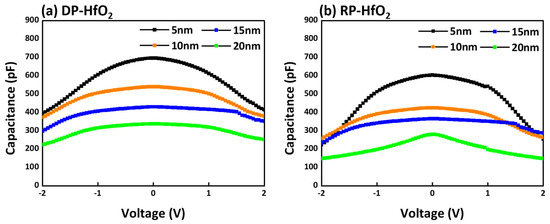
Figure 7.
Capacitance measurement results for 5–20 nm HfO2 samples fabricated via DP-ALD and RP-ALD, using electrodes with a diameter of 200 μm.
Figure 8 illustrates the relationship between the physical thickness (tphy) and the equivalent oxide thickness (EOT) of HfO2 thin films in metal–insulator–metal (MIM) structures as a function of the deposition method. The two deposition methods compared are DP-ALD and RP-ALD. EOT values were calculated using Equation (1), with the physical thickness of the HfO2 films ranging from 5 to 20 nm.
where εhigh-K is the dielectric constant of HfO2, and thigh-K is the thickness of the HfO2 layer.
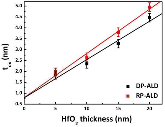
Figure 8.
EOT measurement results for HfO2 thin films with varying thicknesses fabricated via DP-ALD and RP-ALD.
A linear relationship was observed between EOT and physical thickness (tphy). For the HfO2 films deposited via DP-ALD, linear regression yielded the following equation:
EOT = 0.175 × tphy + 0.79
The slope corresponds to a dielectric constant of approximately 22.2, which reflects the intrinsic permittivity of the HfO2 films, excluding the influence of any interfacial low-k layers. Similarly, for RP-ALD, the relationship is as follows:
where the slope corresponds to a dielectric constant of approximately 19.2. The y-intercepts (0.79 nm for DP and 0.80 nm for RP) can be attributed to interfacial oxidation effects, such as the formation of a fixed interfacial layer composed of SiO2. The variation in extracted dielectric constants may result from differences in film density, crystallinity, or impurity levels introduced by each deposition method. These results highlight the critical role of deposition parameters in determining the electrical performance of high-k dielectric films [9,47,48].
EOT = 0.20 × tphy + 0.80
Figure 9 presents the leakage current characteristics of HfO2 thin films deposited using the DP method (Figure 9a) and the RP method (Figure 9b). Leakage current measurements were conducted by applying voltage from 0 to 5 V in 0.05 V increments. As observed, HfO2 thin films fabricated via DP-ALD exhibited a relatively high leakage current, which can be attributed to the presence of a large number of defects within the film. By contrast, the films deposited by RP-ALD showed significantly reduced leakage current. This difference can be primarily attributed to the distinct plasma generation mechanisms of each process. In the DP-ALD method, plasma discharge occurs directly within the deposition chamber, exposing the film surface to direct plasma bombardment. However, in the RP-ALD method, plasma is generated in a remote chamber, thereby preventing direct plasma exposure to the film surface. As a result, surface damage and defect formation are effectively suppressed, leading to improved electrical performance over the entire voltage range. Specifically, at 0.8 V and a thickness of 15 nm, the DP-HfO2 film exhibited a leakage current density of approximately 10−4 A/cm2, whereas the RP-HfO2 film showed a significantly lower leakage current density of approximately 10−7 A/cm2, demonstrating three orders of magnitude improvement in leakage performance.
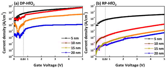
Figure 9.
Current density results for 5–20 nm HfO2 thin films fabricated via (a) DP-ALD and (b) RP-ALD.
Figure 10 presents the leakage current characteristics of HfO2-based capacitors fabricated via DP-ALD and RP-ALD. The plot shows the current density at 0.8 V as a function of equivalent oxide thickness (EOT), categorized by plasma type. For clarity, solid lines are included to guide the eye, and data points are color-coded: black for DP and red for RP. The results demonstrate that, at the same physical thickness, the RP-deposited films exhibit significantly lower leakage currents than their DP counterparts. Specifically, at an EOT of approximately 2.4 nm, the HfO2 capacitor fabricated via the RP process exhibits a leakage current density of approximately 1 × 10⁻⁶ A/cm2, whereas the DP-processed counterpart exhibits a considerably higher value of approximately 9 × 10⁻⁴ A/cm2. These findings indicate that the RP-ALD process induces substantially fewer plasma-related defects, resulting in a reduced number of interface and bulk defects. Consequently, superior leakage performance can be achieved even at comparable EOT levels.
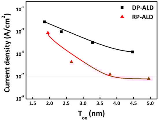
Figure 10.
Current densities of HfO2 thin films fabricated via DP-ALD and RP-ALD as a function of EOT.
4. Conclusions
In this work, we investigated and compared the characteristics of HfO2 thin films deposited on trench-structured silicon substrates using DP-ALD and RP-ALD. While DP-ALD achieved higher deposition rates, RP-ALD offered superior conformality and film uniformity, achieving nearly 100% step coverage regardless of trench orientation. XPS analysis confirmed the presence of a higher density of non-lattice Hf and oxygen-related defects in DP-ALD films, attributable to direct plasma exposure. These defects resulted in increased leakage current, despite a slight enhancement in capacitance due to the defect–polarization effect. By contrast, RP-ALD significantly suppressed defect formation by eliminating direct plasma contact, thereby significantly improving dielectric reliability and reducing leakage current at equivalent EOT. Overall, although DP-ALD is advantageous for productivity, RP-ALD demonstrates distinct benefits in terms of film quality and electrical performance. These findings highlight the importance of plasma configuration in ALD processes and establish RP-ALD as a more suitable technique for the reliable integration of high-k dielectrics in advanced DRAM capacitor applications. Furthermore, this study is limited to HfO2 and a specific trench structure. Future research investigating the applicability of this process to various high-k materials and more complex 3D structures with high aspect ratios (e.g., 100:1), along with evaluations of long-term reliability and in-depth analyses of defect formation mechanisms, could enable the extension of this technique to next-generation plasma-based dielectric processes for DRAM applications.
Author Contributions
Conceptualization, J.K. and I.H.; methodology, J.K., B.K. and W.L.; validation, Y.J. and C.Y.; investigation, J.K. and I.H.; writing—original draft preparation, B.K., J.S. and C.Y.; writing—review and editing, W.L., J.S. and Y.J.; All authors have read and agreed to the published version of the manuscript.
Funding
This work was supported by K-CHIPS (Korea Collaborative & High-tech Initiative for Prospective Semiconductor Research) (2410000308, RS-2023-00237030, 23027-15FC), funded by the Ministry of Trade, Industry, and Energy (MOTIE, Republic of Korea).
Data Availability Statement
Data are contained within the article.
Conflicts of Interest
The authors declare no conflicts of interest. The funder had no role in the design of the study; in the collection, analyses, or interpretation of the data; in the writing of the manuscript; or in the decision to publish the results.
Abbreviations
The following abbreviations are used in this manuscript:
| CD | critical dimension |
| DRAM | dynamic random-access memory |
| ALD | atomic layer deposition |
| MIM | metal–insulator–metal |
| RP-ALD | remote plasma ALD |
| DP-ALD | direct plasma ALD |
| EOT | equivalent oxide thickness |
| ZAZ | ZrO2/Al2O3/ZrO2 |
References
- Smitha, P.S.; Babu, V.S.; Shiny, G. Critical parameters of high performance metal-insulator-metal nanocapacitors: A Review. Mater. Res. Express 2019, 6, 122003. [Google Scholar] [CrossRef]
- An, C.H.; Lee, W.; Kim, S.H.; Cho, C.J.; Kim, D.-G.; Kwon, D.S.; Cho, S.T.; Cha, S.H.; Lim, J.I.; Jeon, W.; et al. Controlling the electrical characteristics of ZrO2/Al2O3/ZrO2 capacitors by adopting a Ru top electrode grown via atomic layer deposition. Phys. Status Solidi (RRL)–Rapid Res. Lett. 2019, 13, 1800454. [Google Scholar] [CrossRef]
- Zheng, G.; He, Y.-L.; Zhu, B.; Wu, X.; Zhang, D.W.; Ding, S.-J. Improvement of voltage linearity and leakage current of MIM capacitors with atomic layer deposited Ti-doped ZrO2 insulators. IEEE Trans. Electron. Devices 2023, 70, 3064–3070. [Google Scholar] [CrossRef]
- Cho, H.J.; Kim, Y.D.; Park, D.S.; Lee, E.; Park, C.H.; Jang, J.S.; Lee, K.B.; Kim, H.W.; Chae, S.J.; Ki, Y.J.; et al. New TIT capacitor with ZrO2/Al2O3/ZrO2 dielectrics for 60 nm and below DRAMs. In Proceedings of the 2006 European Solid-State Device Research Conference, Montreux, Switzerland, 19–21 September 2006; pp. 146–149. [Google Scholar]
- Xiong, L.; Hu, J.; Yang, Z.; Li, X.; Zhang, H.; Zhang, G. Dielectric properties investigation of metal–insulator–metal (MIM) capacitors. Molecules 2022, 27, 3951. [Google Scholar] [CrossRef] [PubMed]
- Weinreich, W.; Shariq, A.; Seidel, K.; Sundqvist, J.; Paskaleva, A.; Lemberger, M.; Bauer, A.J. Detailed leakage current analysis of metal–insulator–metal capacitors with ZrO2, ZrO2/SiO2/ZrO2, and ZrO2/Al2O3/ZrO2 as dielectric and TiN electrodes. J. Vac. Sci. Technol. B 2012, 31, 01A109. [Google Scholar] [CrossRef]
- Cho, S.T.; An, C.H.; Kim, S.H.; Kim, D.G.; Kwon, D.S.; Cha, S.H.; Hwang, C.S. Electrical and structural properties of ZrO2/Y2O3/ZrO2 dielectric film for DRAM capacitor. Meet. Abstr. 2018, MA2018-01, 2524. [Google Scholar] [CrossRef]
- Huang, C.; Cheng, C.-H.; Lee, K.; Liou, B.-H. Performance improvement of metal–insulator–metal capacitors using postmetallization-annealed treatment on the Al2O3/TiO2/Al2O3 film. Electrochem. Solid-State Lett. 2009, 12, H123. [Google Scholar] [CrossRef]
- Ogawa, A.; Iwamoto, K.; Ota, H.; Morita, Y.; Ikeda, M.; Nabatame, T.; Toriumi, A. 0.6 nm-EOT high-k gate stacks with HfSiOx interfacial layer grown by solid-phase reaction between HfO2 and Si substrate. Microelectron. Eng. 2007, 84, 1861–1864. [Google Scholar] [CrossRef]
- Gordon, R.G.; Hausmann, D.; Kim, E.; Shepard, J. A kinetic model for step coverage by atomic layer deposition in narrow holes or trenches. Chem. Vap. Depos. 2003, 9, 73–78. [Google Scholar] [CrossRef]
- Loh, G.H. 3D-stacked memory architectures for multi-core processors. In Proceedings of the 2008 International Symposium on Computer Architecture, Beijing, China, 21–25 June 2008; pp. 453–464. [Google Scholar]
- Song, J.Y.; Choi, W.Y.; Park, J.H.; Lee, J.D.; Park, B.G. Design optimization of gate-all-around (GAA) MOSFETs. IEEE Trans. Nanotechnol. 2006, 5, 186–191. [Google Scholar] [CrossRef]
- Polakowski, P.; Riedel, S.; Weinreich, W.; Rudolf, M.; Sundqvist, J.; Seidel, K.; Muller, J. Ferroelectric deep trench capacitors based on Al:HfO2 for 3D nonvolatile memory applications. In Proceedings of the 2014 IEEE 6th International Memory Workshop (IMW), Taipei, Taiwan, 18–21 May 2014; pp. 1–4. [Google Scholar]
- Das, R.R.; Rajalekshmi, T.R.; James, A. FinFET to GAA MBCFET: A Review and Insights. IEEE Access 2024, 12, 50556–50577. [Google Scholar] [CrossRef]
- Nagy, D.; Indalecio, G.; Garcia-Loureiro, A.J.; Elmessary, M.A.; Kalna, K.; Seoane, N. FinFET versus gate-all-around nanowire FET: Performance, scaling, and variability. IEEE J. Electron. Devices Soc. 2018, 6, 332–340. [Google Scholar] [CrossRef]
- Choi, J.H.; Mao, Y.; Chang, J.P. Development of hafnium based high-k materials—A review. Mater. Sci. Eng. R Rep. 2011, 72, 97–136. [Google Scholar] [CrossRef]
- Lee, W.; An, C.H.; Yoo, S.; Jeon, W.; Chung, M.J.; Kim, S.H.; Hwang, C.S. Electrical properties of ZrO2/Al2O3/ZrO2-based capacitors with TiN, Ru, and TiN/Ru top electrode materials. Phys. Status Solidi (RRL)–Rapid Res. Lett. 2018, 12, 1800356. [Google Scholar] [CrossRef]
- Lee, S.; Han, G.; Kim, K.H.; Shim, D.; Go, D.; An, J. High-performance TiO2/ZrO2/TiO2 thin film capacitor by plasma-assisted atomic layer annealing. ACS Appl. Mater. Interfaces 2024, 16, 34419–34427. [Google Scholar] [CrossRef]
- Martin, D.; Grube, M.; Weinreich, W.; Müller, J.; Wilde, L.; Erben, E.; Weber, W.M.; Heitmann, J.; Schröder, U.; Mikolajick, T.; et al. Macroscopic and microscopic electrical characterizations of high-k ZrO2 and ZrO2/Al2O3/ZrO2 metal-insulator-metal structures. J. Vac. Sci. Technol. B 2011, 29, 01AC02. [Google Scholar] [CrossRef]
- Khaldi, O.; Jomni, F.; Gonon, P.; Vallée, C. AC and DC bias effect on capacitance–voltage nonlinearities in Au/HfO2/M (M = Pt, TiN, W, and AlCu) MIM capacitors: Effect of the bottom electrode material. J. Mater. Sci. Mater. Electron. 2020, 31, 19036–19043. [Google Scholar] [CrossRef]
- Kim, S.K.; Choi, G.-J.; Lee, S.Y.; Seo, M.; Lee, S.W.; Han, J.H.; Ahn, H.-S.; Han, S.; Hwang, C.S. Al-doped TiO2 films with ultralow leakage currents for next generation DRAM capacitors. Adv. Mater. 2008, 20, 1429–1435. [Google Scholar] [CrossRef]
- Kim, J.-H.; Ignatova, V.A.; Heitmann, J.; Oberbeck, L. Deposition temperature effect on electrical properties and interface of high-k ZrO2 capacitor. J. Phys. D Appl. Phys. 2008, 41, 172005. [Google Scholar] [CrossRef]
- Jeong, J.; Han, Y.; Sohn, H. Effect of La doping on dielectric constant and tetragonality of ZrO2 thin films deposited by atomic layer deposition. J. Alloys Compd. 2022, 927, 166961. [Google Scholar] [CrossRef]
- Wei, D.; Hossain, T.; Garces, N.Y.; Nepal, N.; Meyer, H.M.; Kirkham, M.J.; Eddy, C.R.; Edgar, J.H. Influence of atomic layer deposition temperatures on TiO2/n-Si MOS capacitor. ECS J. Solid State Sci. Technol. 2013, 2, N110. [Google Scholar] [CrossRef]
- George, S.M. Atomic layer deposition: An overview. Chem. Rev. 2010, 110, 111–131. [Google Scholar] [CrossRef] [PubMed]
- Martínez-Puente, M.A.; Horley, P.; Aguirre-Tostado, F.S.; López-Medina, J.; Borbón-Nuñez, H.A.; Tiznado, H.; Susarrey-Arce, A.; Martínez-Guerra, E. ALD and PEALD deposition of HfO2 and its effects on the nature of oxygen vacancies. Mater. Sci. Eng. B 2022, 285, 115964. [Google Scholar] [CrossRef]
- Kim, K.; Oh, I.-K.; Kim, H.; Lee, Z. Atomic-scale characterization of plasma-induced damage in plasma-enhanced atomic layer deposition. Appl. Surf. Sci. 2017, 425, 781–787. [Google Scholar] [CrossRef]
- Kim, J.; Kim, S.; Jeon, H.; Cho, M.-H.; Chung, K.-B.; Bae, C. Characteristics of HfO2 thin films grown by plasma atomic layer deposition. Appl. Phys. Lett. 2005, 87, 053108. [Google Scholar] [CrossRef]
- Ahadi, K.; Cadien, K. Ultra low density of interfacial traps with mixed thermal and plasma enhanced ALD of high-κ gate dielectrics. RSC Adv. 2016, 6, 16301–16307. [Google Scholar] [CrossRef]
- Knoops, H.C.M.; Faraz, T.; Arts, K.; Kessels, W.M.M. Status and prospects of plasma-assisted atomic layer deposition. J. Vac. Sci. Technol. A 2019, 37, 030902. [Google Scholar] [CrossRef]
- Lo Nigro, R.; Schilirò, E.; Mannino, G.; Di Franco, S.; Roccaforte, F. Comparison between thermal and plasma enhanced atomic layer deposition processes for the growth of HfO2 dielectric layers. J. Cryst. Growth 2020, 539, 125624. [Google Scholar] [CrossRef]
- Profijt, H.B.; Potts, S.E.; van de Sanden, M.C.M.; Kessels, W.M.M. Plasma-assisted atomic layer deposition: Basics, opportunities, and challenges. J. Vac. Sci. Technol. A 2011, 29, 050801. [Google Scholar] [CrossRef]
- Heil, S.B.S.; van Hemmen, J.L.; Hodson, C.J.; Singh, N.; Klootwijk, J.H.; Roozeboom, F.; van de Sanden, M.C.M.; Kessels, W.M.M. Deposition of TiN and HfO2 in a commercial 200 mm remote plasma atomic layer deposition reactor. J. Vac. Sci. Technol. A 2007, 25, 1357–1366. [Google Scholar] [CrossRef]
- Zhang, X.-Y.; Yang, Y.; Zhang, Z.-X.; Geng, X.-P.; Hsu, C.-H.; Wu, W.-Y.; Lien, S.-Y.; Zhu, W.-Z. Deposition and characterization of RP-ALD SiO2 thin films with different oxygen plasma powers. Nanomaterials 2021, 11, 1173. [Google Scholar] [CrossRef] [PubMed]
- Yoo, J.-H.; Park, W.-J.; Kim, S.-W.; Lee, G.-R.; Kim, J.-H.; Lee, J.-H.; Uhm, S.-H.; Lee, H.-C. Preparation of remote plasma atomic layer-deposited HfO2 thin films with high charge trapping densities and their application in nonvolatile memory devices. Nanomaterials 2023, 13, 1785. [Google Scholar] [CrossRef]
- Renault, O.; Samour, D.; Damlencourt, J.-F.; Blin, D.; Martin, F.; Marthon, S.; Barrett, N.T.; Besson, P. HfO2/SiO2 interface chemistry studied by synchrotron radiation X-ray photoelectron spectroscopy. Appl. Phys. Lett. 2002, 81, 3627–3629. [Google Scholar] [CrossRef]
- Robertson, J.; Wallace, R.M. High-k materials and metal gates for CMOS applications. Mater. Sci. Eng. R Rep. 2015, 88, 1–41. [Google Scholar] [CrossRef]
- Foster, A.S.; Lopez Gejo, F.; Shluger, A.L.; Nieminen, R.M. Vacancy and interstitial defects in hafnia. Phys. Rev. B 2002, 65, 174117. [Google Scholar] [CrossRef]
- Driemeier, C.; Wallace, R.M.; Baumvol, I.J.R. Oxygen species in HfO2 films: An in situ X-ray photoelectron spectroscopy study. J. Appl. Phys. 2007, 102, 024112. [Google Scholar] [CrossRef]
- Morant, C.; Galán, L.; Sanz, J.M. An XPS study of the initial stages of oxidation of hafnium. Surf. Interface Anal. 1990, 16, 304–308. [Google Scholar] [CrossRef]
- Castagné, R.; Vapaille, A. Description of the SiO2–Si interface properties by means of very low frequency MOS capacitance measurements. Surf. Sci. 1971, 28, 157–193. [Google Scholar] [CrossRef]
- Choi, M.; Lyons, J.L.; Janotti, A.; Van de Walle, C. Impact of carbon and nitrogen impurities in high-κ dielectrics on metal-oxide-semiconductor devices. Appl. Phys. Lett. 2013, 102, 142902. [Google Scholar] [CrossRef]
- Bertóti, I.; Mohai, M.; Sullivan, J.L.; Saied, S.O. Surface characterisation of plasma-nitrided titanium: An XPS study. Appl. Surf. Sci. 1995, 84, 357–371. [Google Scholar] [CrossRef]
- Cho, D.-Y.; Oh, S.-J.; Chang, Y.J.; Noh, T.W.; Jung, R.; Lee, J.-C. Role of oxygen vacancy in HfO2∕SiO2∕Si(100) interfaces. Appl. Phys. Lett. 2006, 88, 193502. [Google Scholar] [CrossRef]
- Cockayne, E. Influence of oxygen vacancies on the dielectric properties of hafnia: First-principles calculations. Phys. Rev. B 2007, 75, 094103. [Google Scholar] [CrossRef]
- Zhang, W.D.; Song, Z.Z.; Tang, S.Q.; Wei, J.C.; Cheng, Y.; Li, B.; Chen, S.Y.; Chen, Z.B.; Jiang, A.Q. Ultrahigh dielectric permittivity in Hf0.5Zr0.5O2 thin-film capacitors. Nat. Commun. 2025, 16, 2679. [Google Scholar] [CrossRef] [PubMed]
- Kang, Y.-S.; Kang, H.-K.; Kim, D.-K.; Jeong, K.-S.; Baik, M.; An, Y.; Kim, H.; Song, J.-D.; Cho, M.-H. Structural and electrical properties of EOT HfO2 (<1 nm) grown on InAs by atomic layer deposition and its thermal stability. ACS Appl. Mater. Interfaces 2016, 8, 7489–7498. [Google Scholar] [CrossRef]
- Kim, B.Y.; Lee, I.S.; Park, H.W.; Lee, Y.B.; Lee, S.H.; Oh, M.; Ryoo, S.K.; Byun, S.R.; Kim, K.D.; Lee, J.H.; et al. Top electrode engineering for high-performance ferroelectric Hf0.5Zr0.5O2 capacitors. Adv. Mater. Technol. 2023, 8, 2300146. [Google Scholar] [CrossRef]
Disclaimer/Publisher’s Note: The statements, opinions and data contained in all publications are solely those of the individual author(s) and contributor(s) and not of MDPI and/or the editor(s). MDPI and/or the editor(s) disclaim responsibility for any injury to people or property resulting from any ideas, methods, instructions or products referred to in the content. |
© 2025 by the authors. Licensee MDPI, Basel, Switzerland. This article is an open access article distributed under the terms and conditions of the Creative Commons Attribution (CC BY) license (https://creativecommons.org/licenses/by/4.0/).