
Deposition of HfO2 by Remote Plasma ALD for High-Aspect-Ratio Trench Capacitors in DRAM


Abstract

1. Introduction
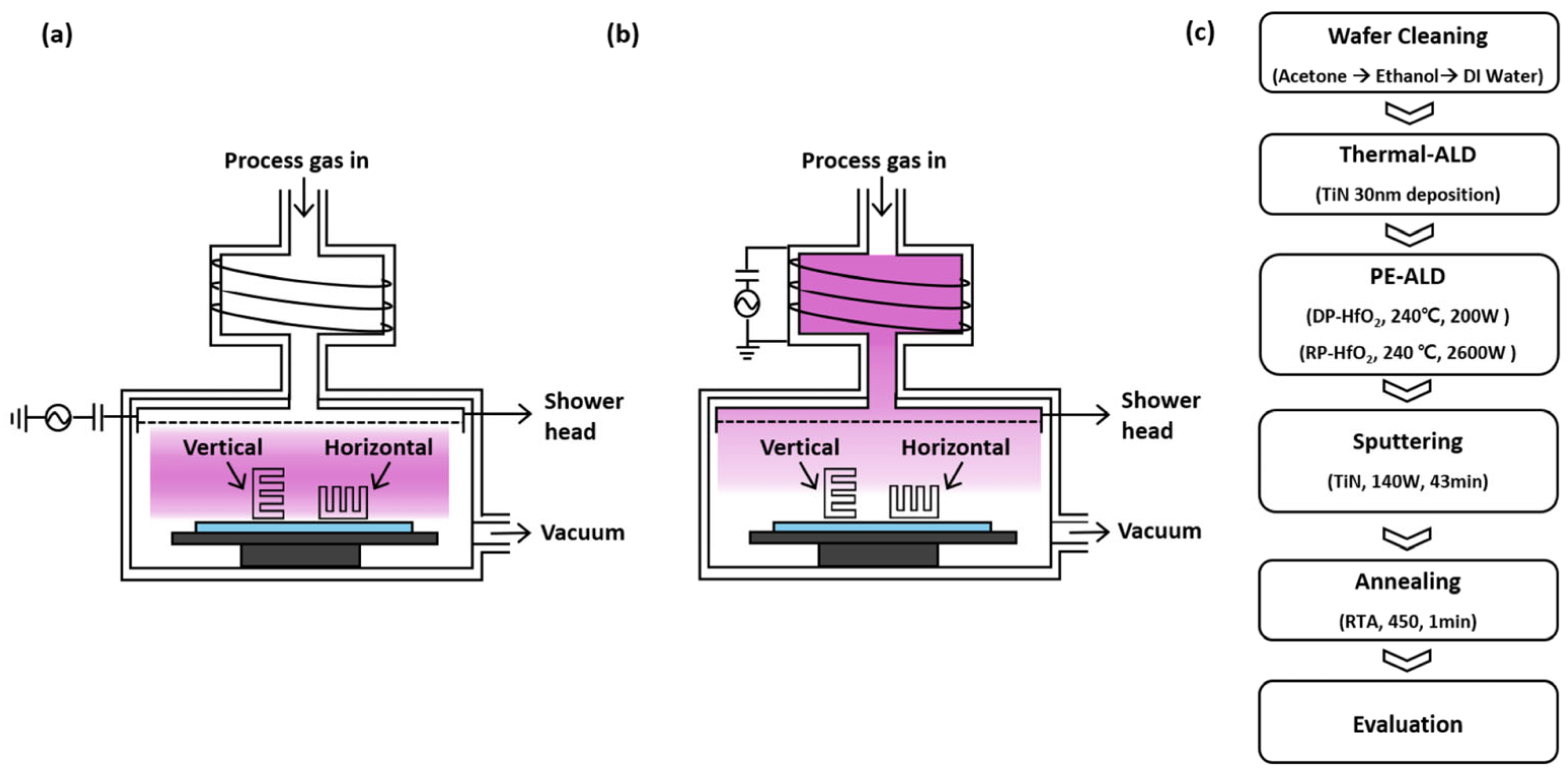
2. Materials and Methods
2.1. Deposition of HfO2 Thin Films Using RP-ALD and DP-ALD
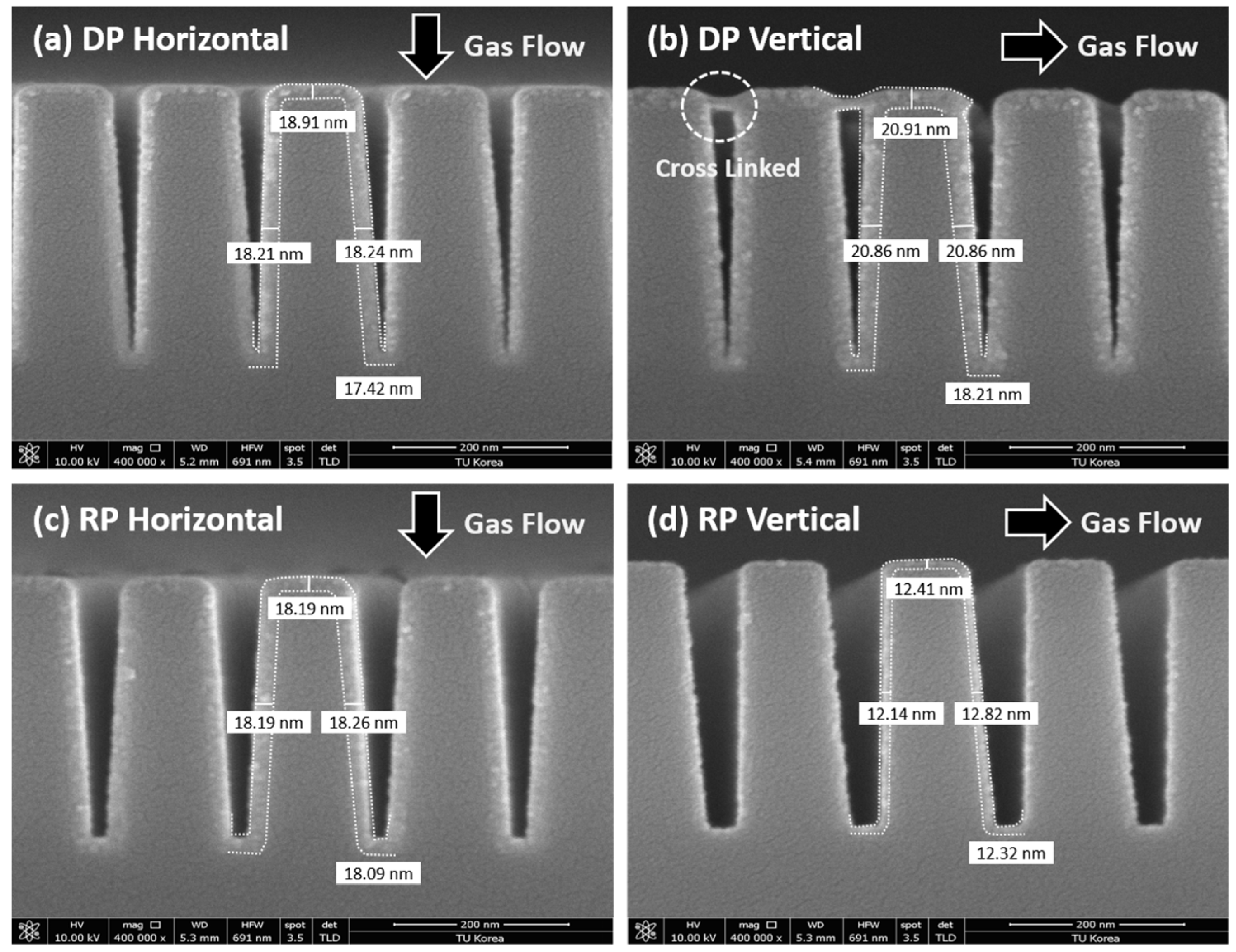
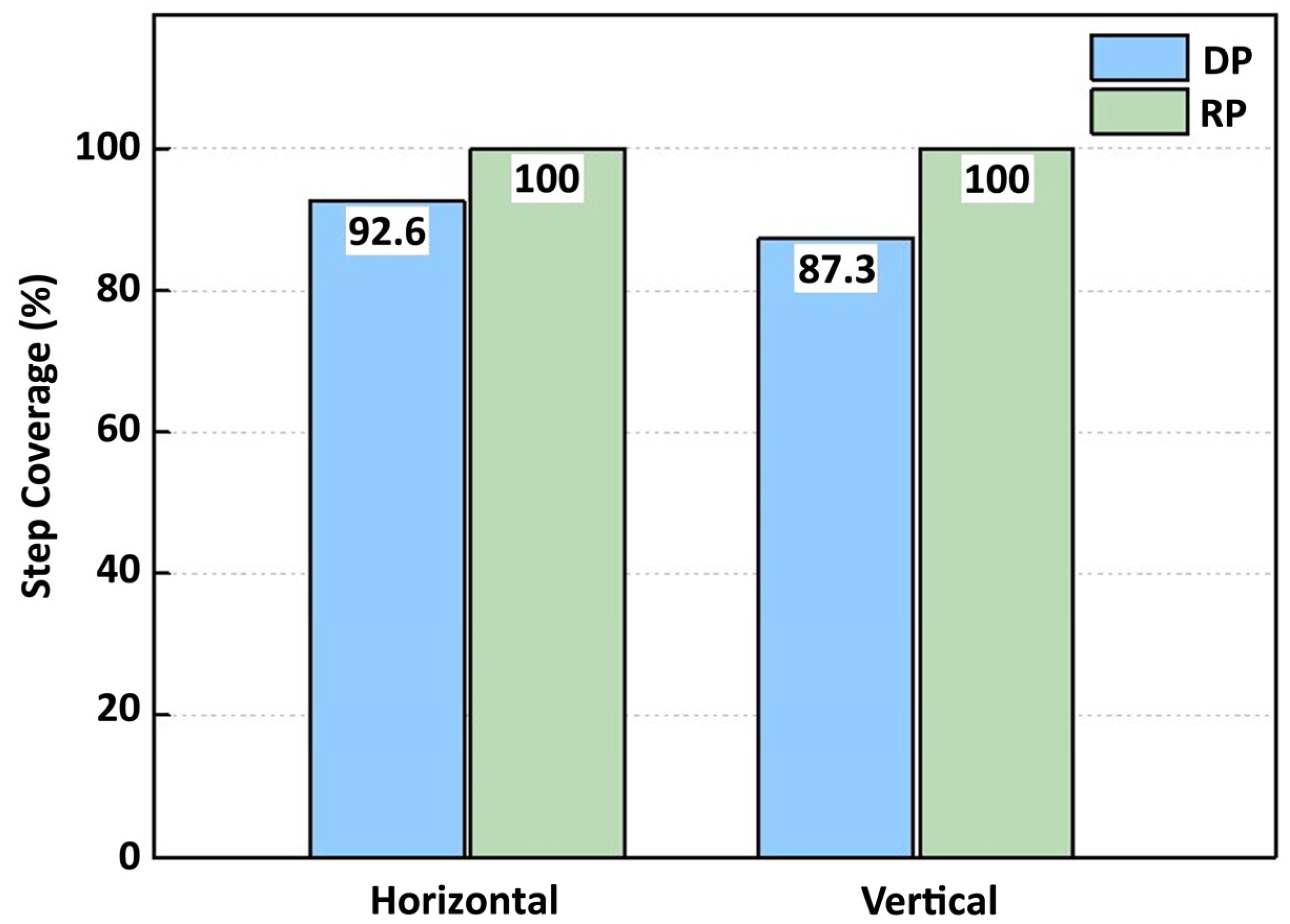
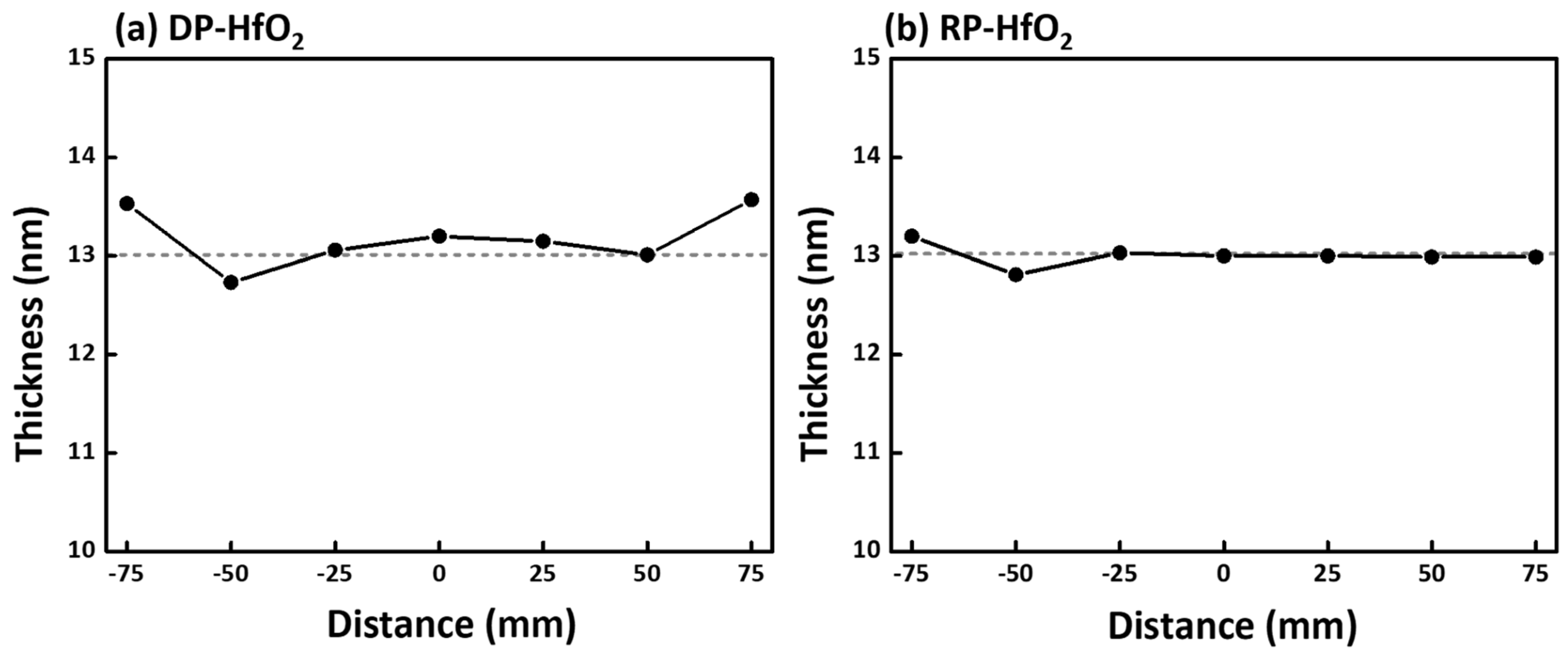
2.2. Evaluation of the Properties of Trenches Deposited by DP and RP-ALD
3. Results
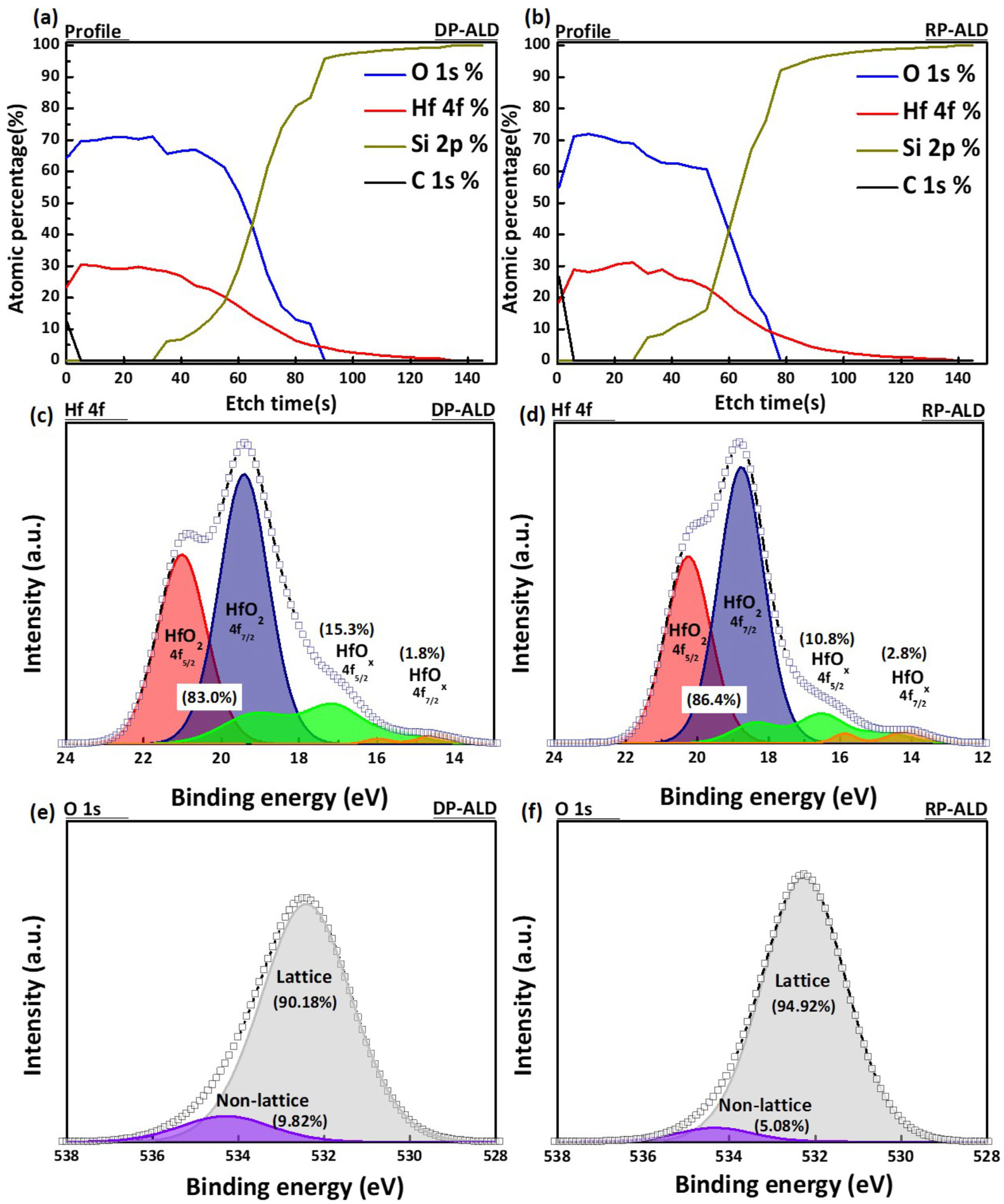
3.1. Characteristics of HfO2 Thin Films Deposited by DP-ALD and RP-ALD
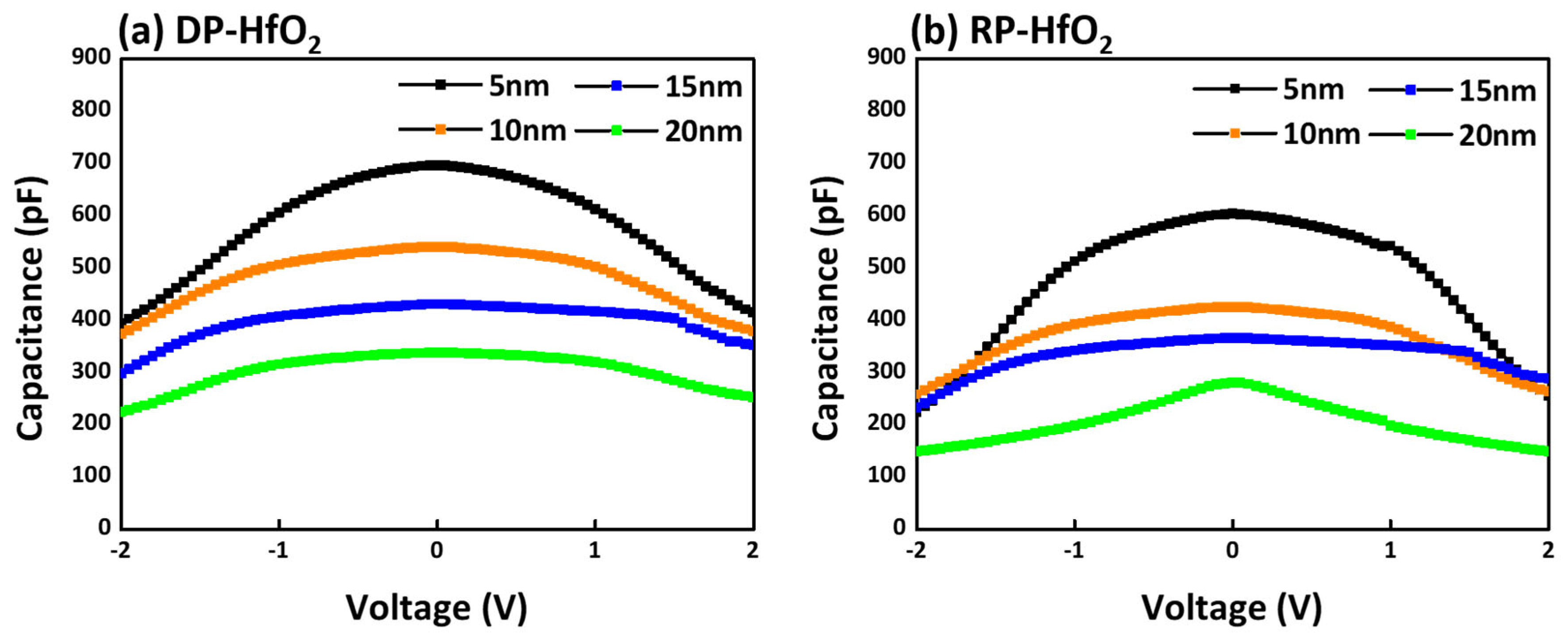
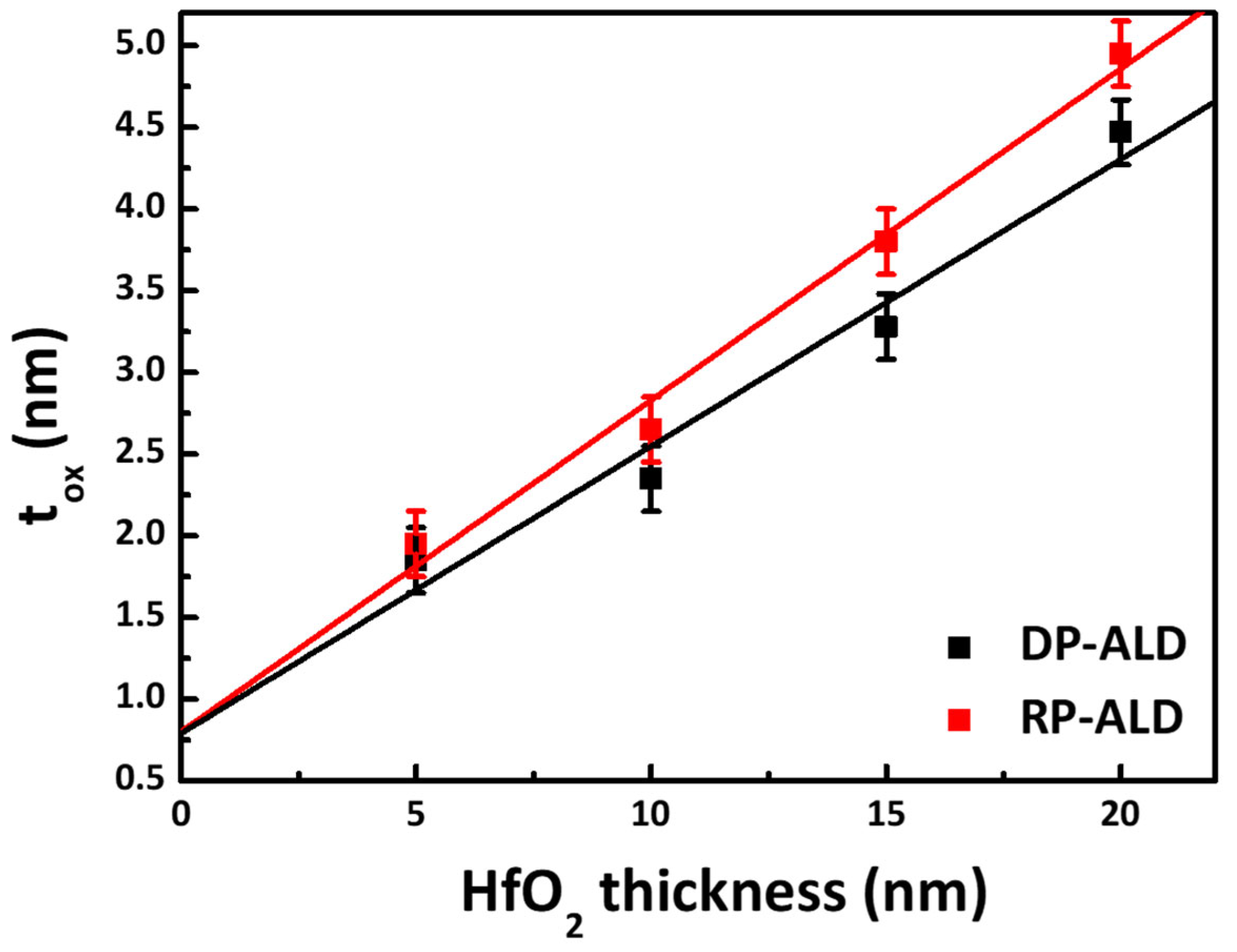
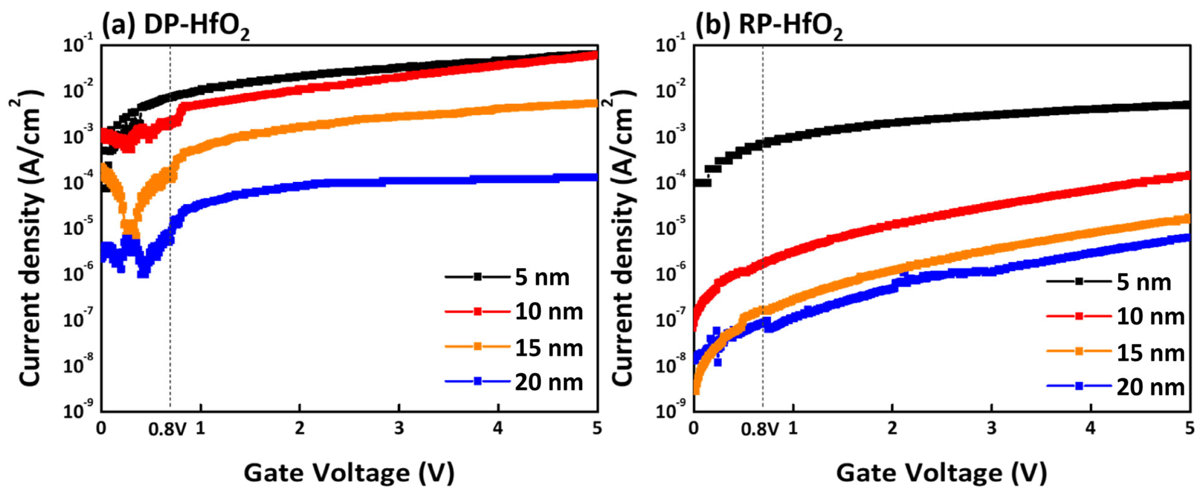
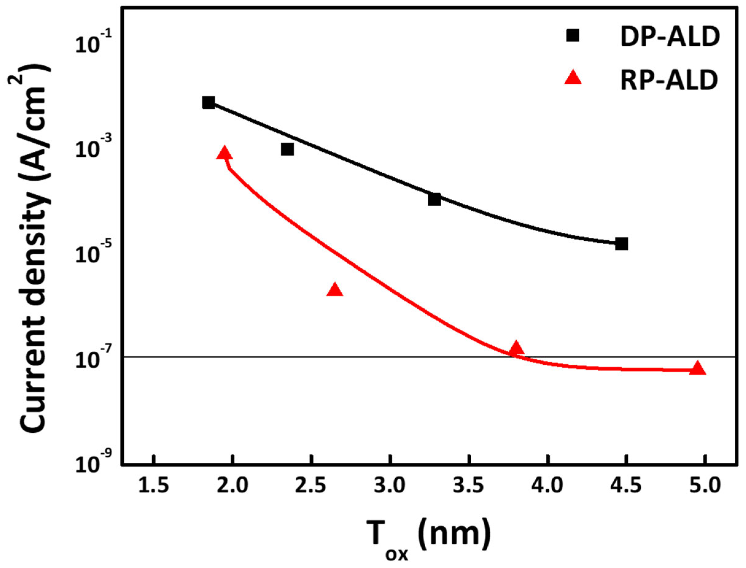
3.2. MIM Device Electrical Characteristics
4. Conclusions
Author Contributions
Funding
Data Availability Statement
Conflicts of Interest
Abbreviations
| CD | critical dimension |
| DRAM | dynamic random-access memory |
| ALD | atomic layer deposition |
| MIM | metal–insulator–metal |
| RP-ALD | remote plasma ALD |
| DP-ALD | direct plasma ALD |
| EOT | equivalent oxide thickness |
| ZAZ | ZrO2/Al2O3/ZrO2 |
References
- Smitha, P.S.; Babu, V.S.; Shiny, G. Critical parameters of high performance metal-insulator-metal nanocapacitors: A Review. Mater. Res. Express 2019, 6, 122003. [Google Scholar] [CrossRef]
- An, C.H.; Lee, W.; Kim, S.H.; Cho, C.J.; Kim, D.-G.; Kwon, D.S.; Cho, S.T.; Cha, S.H.; Lim, J.I.; Jeon, W.; et al. Controlling the electrical characteristics of ZrO2/Al2O3/ZrO2 capacitors by adopting a Ru top electrode grown via atomic layer deposition. Phys. Status Solidi (RRL)–Rapid Res. Lett. 2019, 13, 1800454. [Google Scholar] [CrossRef]
- Zheng, G.; He, Y.-L.; Zhu, B.; Wu, X.; Zhang, D.W.; Ding, S.-J. Improvement of voltage linearity and leakage current of MIM capacitors with atomic layer deposited Ti-doped ZrO2 insulators. IEEE Trans. Electron. Devices 2023, 70, 3064–3070. [Google Scholar] [CrossRef]
- Cho, H.J.; Kim, Y.D.; Park, D.S.; Lee, E.; Park, C.H.; Jang, J.S.; Lee, K.B.; Kim, H.W.; Chae, S.J.; Ki, Y.J.; et al. New TIT capacitor with ZrO2/Al2O3/ZrO2 dielectrics for 60 nm and below DRAMs. In Proceedings of the 2006 European Solid-State Device Research Conference, Montreux, Switzerland, 19–21 September 2006; pp. 146–149. [Google Scholar]
- Xiong, L.; Hu, J.; Yang, Z.; Li, X.; Zhang, H.; Zhang, G. Dielectric properties investigation of metal–insulator–metal (MIM) capacitors. Molecules 2022, 27, 3951. [Google Scholar] [CrossRef] [PubMed]
- Weinreich, W.; Shariq, A.; Seidel, K.; Sundqvist, J.; Paskaleva, A.; Lemberger, M.; Bauer, A.J. Detailed leakage current analysis of metal–insulator–metal capacitors with ZrO2, ZrO2/SiO2/ZrO2, and ZrO2/Al2O3/ZrO2 as dielectric and TiN electrodes. J. Vac. Sci. Technol. B 2012, 31, 01A109. [Google Scholar] [CrossRef]
- Cho, S.T.; An, C.H.; Kim, S.H.; Kim, D.G.; Kwon, D.S.; Cha, S.H.; Hwang, C.S. Electrical and structural properties of ZrO2/Y2O3/ZrO2 dielectric film for DRAM capacitor. Meet. Abstr. 2018, MA2018-01, 2524. [Google Scholar] [CrossRef]
- Huang, C.; Cheng, C.-H.; Lee, K.; Liou, B.-H. Performance improvement of metal–insulator–metal capacitors using postmetallization-annealed treatment on the Al2O3/TiO2/Al2O3 film. Electrochem. Solid-State Lett. 2009, 12, H123. [Google Scholar] [CrossRef]
- Ogawa, A.; Iwamoto, K.; Ota, H.; Morita, Y.; Ikeda, M.; Nabatame, T.; Toriumi, A. 0.6 nm-EOT high-k gate stacks with HfSiOx interfacial layer grown by solid-phase reaction between HfO2 and Si substrate. Microelectron. Eng. 2007, 84, 1861–1864. [Google Scholar] [CrossRef]
- Gordon, R.G.; Hausmann, D.; Kim, E.; Shepard, J. A kinetic model for step coverage by atomic layer deposition in narrow holes or trenches. Chem. Vap. Depos. 2003, 9, 73–78. [Google Scholar] [CrossRef]
- Loh, G.H. 3D-stacked memory architectures for multi-core processors. In Proceedings of the 2008 International Symposium on Computer Architecture, Beijing, China, 21–25 June 2008; pp. 453–464. [Google Scholar]
- Song, J.Y.; Choi, W.Y.; Park, J.H.; Lee, J.D.; Park, B.G. Design optimization of gate-all-around (GAA) MOSFETs. IEEE Trans. Nanotechnol. 2006, 5, 186–191. [Google Scholar] [CrossRef]
- Polakowski, P.; Riedel, S.; Weinreich, W.; Rudolf, M.; Sundqvist, J.; Seidel, K.; Muller, J. Ferroelectric deep trench capacitors based on Al:HfO2 for 3D nonvolatile memory applications. In Proceedings of the 2014 IEEE 6th International Memory Workshop (IMW), Taipei, Taiwan, 18–21 May 2014; pp. 1–4. [Google Scholar]
- Das, R.R.; Rajalekshmi, T.R.; James, A. FinFET to GAA MBCFET: A Review and Insights. IEEE Access 2024, 12, 50556–50577. [Google Scholar] [CrossRef]
- Nagy, D.; Indalecio, G.; Garcia-Loureiro, A.J.; Elmessary, M.A.; Kalna, K.; Seoane, N. FinFET versus gate-all-around nanowire FET: Performance, scaling, and variability. IEEE J. Electron. Devices Soc. 2018, 6, 332–340. [Google Scholar] [CrossRef]
- Choi, J.H.; Mao, Y.; Chang, J.P. Development of hafnium based high-k materials—A review. Mater. Sci. Eng. R Rep. 2011, 72, 97–136. [Google Scholar] [CrossRef]
- Lee, W.; An, C.H.; Yoo, S.; Jeon, W.; Chung, M.J.; Kim, S.H.; Hwang, C.S. Electrical properties of ZrO2/Al2O3/ZrO2-based capacitors with TiN, Ru, and TiN/Ru top electrode materials. Phys. Status Solidi (RRL)–Rapid Res. Lett. 2018, 12, 1800356. [Google Scholar] [CrossRef]
- Lee, S.; Han, G.; Kim, K.H.; Shim, D.; Go, D.; An, J. High-performance TiO2/ZrO2/TiO2 thin film capacitor by plasma-assisted atomic layer annealing. ACS Appl. Mater. Interfaces 2024, 16, 34419–34427. [Google Scholar] [CrossRef]
- Martin, D.; Grube, M.; Weinreich, W.; Müller, J.; Wilde, L.; Erben, E.; Weber, W.M.; Heitmann, J.; Schröder, U.; Mikolajick, T.; et al. Macroscopic and microscopic electrical characterizations of high-k ZrO2 and ZrO2/Al2O3/ZrO2 metal-insulator-metal structures. J. Vac. Sci. Technol. B 2011, 29, 01AC02. [Google Scholar] [CrossRef]
- Khaldi, O.; Jomni, F.; Gonon, P.; Vallée, C. AC and DC bias effect on capacitance–voltage nonlinearities in Au/HfO2/M (M = Pt, TiN, W, and AlCu) MIM capacitors: Effect of the bottom electrode material. J. Mater. Sci. Mater. Electron. 2020, 31, 19036–19043. [Google Scholar] [CrossRef]
- Kim, S.K.; Choi, G.-J.; Lee, S.Y.; Seo, M.; Lee, S.W.; Han, J.H.; Ahn, H.-S.; Han, S.; Hwang, C.S. Al-doped TiO2 films with ultralow leakage currents for next generation DRAM capacitors. Adv. Mater. 2008, 20, 1429–1435. [Google Scholar] [CrossRef]
- Kim, J.-H.; Ignatova, V.A.; Heitmann, J.; Oberbeck, L. Deposition temperature effect on electrical properties and interface of high-k ZrO2 capacitor. J. Phys. D Appl. Phys. 2008, 41, 172005. [Google Scholar] [CrossRef]
- Jeong, J.; Han, Y.; Sohn, H. Effect of La doping on dielectric constant and tetragonality of ZrO2 thin films deposited by atomic layer deposition. J. Alloys Compd. 2022, 927, 166961. [Google Scholar] [CrossRef]
- Wei, D.; Hossain, T.; Garces, N.Y.; Nepal, N.; Meyer, H.M.; Kirkham, M.J.; Eddy, C.R.; Edgar, J.H. Influence of atomic layer deposition temperatures on TiO2/n-Si MOS capacitor. ECS J. Solid State Sci. Technol. 2013, 2, N110. [Google Scholar] [CrossRef]
- George, S.M. Atomic layer deposition: An overview. Chem. Rev. 2010, 110, 111–131. [Google Scholar] [CrossRef] [PubMed]
- Martínez-Puente, M.A.; Horley, P.; Aguirre-Tostado, F.S.; López-Medina, J.; Borbón-Nuñez, H.A.; Tiznado, H.; Susarrey-Arce, A.; Martínez-Guerra, E. ALD and PEALD deposition of HfO2 and its effects on the nature of oxygen vacancies. Mater. Sci. Eng. B 2022, 285, 115964. [Google Scholar] [CrossRef]
- Kim, K.; Oh, I.-K.; Kim, H.; Lee, Z. Atomic-scale characterization of plasma-induced damage in plasma-enhanced atomic layer deposition. Appl. Surf. Sci. 2017, 425, 781–787. [Google Scholar] [CrossRef]
- Kim, J.; Kim, S.; Jeon, H.; Cho, M.-H.; Chung, K.-B.; Bae, C. Characteristics of HfO2 thin films grown by plasma atomic layer deposition. Appl. Phys. Lett. 2005, 87, 053108. [Google Scholar] [CrossRef]
- Ahadi, K.; Cadien, K. Ultra low density of interfacial traps with mixed thermal and plasma enhanced ALD of high-κ gate dielectrics. RSC Adv. 2016, 6, 16301–16307. [Google Scholar] [CrossRef]
- Knoops, H.C.M.; Faraz, T.; Arts, K.; Kessels, W.M.M. Status and prospects of plasma-assisted atomic layer deposition. J. Vac. Sci. Technol. A 2019, 37, 030902. [Google Scholar] [CrossRef]
- Lo Nigro, R.; Schilirò, E.; Mannino, G.; Di Franco, S.; Roccaforte, F. Comparison between thermal and plasma enhanced atomic layer deposition processes for the growth of HfO2 dielectric layers. J. Cryst. Growth 2020, 539, 125624. [Google Scholar] [CrossRef]
- Profijt, H.B.; Potts, S.E.; van de Sanden, M.C.M.; Kessels, W.M.M. Plasma-assisted atomic layer deposition: Basics, opportunities, and challenges. J. Vac. Sci. Technol. A 2011, 29, 050801. [Google Scholar] [CrossRef]
- Heil, S.B.S.; van Hemmen, J.L.; Hodson, C.J.; Singh, N.; Klootwijk, J.H.; Roozeboom, F.; van de Sanden, M.C.M.; Kessels, W.M.M. Deposition of TiN and HfO2 in a commercial 200 mm remote plasma atomic layer deposition reactor. J. Vac. Sci. Technol. A 2007, 25, 1357–1366. [Google Scholar] [CrossRef]
- Zhang, X.-Y.; Yang, Y.; Zhang, Z.-X.; Geng, X.-P.; Hsu, C.-H.; Wu, W.-Y.; Lien, S.-Y.; Zhu, W.-Z. Deposition and characterization of RP-ALD SiO2 thin films with different oxygen plasma powers. Nanomaterials 2021, 11, 1173. [Google Scholar] [CrossRef] [PubMed]
- Yoo, J.-H.; Park, W.-J.; Kim, S.-W.; Lee, G.-R.; Kim, J.-H.; Lee, J.-H.; Uhm, S.-H.; Lee, H.-C. Preparation of remote plasma atomic layer-deposited HfO2 thin films with high charge trapping densities and their application in nonvolatile memory devices. Nanomaterials 2023, 13, 1785. [Google Scholar] [CrossRef]
- Renault, O.; Samour, D.; Damlencourt, J.-F.; Blin, D.; Martin, F.; Marthon, S.; Barrett, N.T.; Besson, P. HfO2/SiO2 interface chemistry studied by synchrotron radiation X-ray photoelectron spectroscopy. Appl. Phys. Lett. 2002, 81, 3627–3629. [Google Scholar] [CrossRef]
- Robertson, J.; Wallace, R.M. High-k materials and metal gates for CMOS applications. Mater. Sci. Eng. R Rep. 2015, 88, 1–41. [Google Scholar] [CrossRef]
- Foster, A.S.; Lopez Gejo, F.; Shluger, A.L.; Nieminen, R.M. Vacancy and interstitial defects in hafnia. Phys. Rev. B 2002, 65, 174117. [Google Scholar] [CrossRef]
- Driemeier, C.; Wallace, R.M.; Baumvol, I.J.R. Oxygen species in HfO2 films: An in situ X-ray photoelectron spectroscopy study. J. Appl. Phys. 2007, 102, 024112. [Google Scholar] [CrossRef]
- Morant, C.; Galán, L.; Sanz, J.M. An XPS study of the initial stages of oxidation of hafnium. Surf. Interface Anal. 1990, 16, 304–308. [Google Scholar] [CrossRef]
- Castagné, R.; Vapaille, A. Description of the SiO2–Si interface properties by means of very low frequency MOS capacitance measurements. Surf. Sci. 1971, 28, 157–193. [Google Scholar] [CrossRef]
- Choi, M.; Lyons, J.L.; Janotti, A.; Van de Walle, C. Impact of carbon and nitrogen impurities in high-κ dielectrics on metal-oxide-semiconductor devices. Appl. Phys. Lett. 2013, 102, 142902. [Google Scholar] [CrossRef]
- Bertóti, I.; Mohai, M.; Sullivan, J.L.; Saied, S.O. Surface characterisation of plasma-nitrided titanium: An XPS study. Appl. Surf. Sci. 1995, 84, 357–371. [Google Scholar] [CrossRef]
- Cho, D.-Y.; Oh, S.-J.; Chang, Y.J.; Noh, T.W.; Jung, R.; Lee, J.-C. Role of oxygen vacancy in HfO2∕SiO2∕Si(100) interfaces. Appl. Phys. Lett. 2006, 88, 193502. [Google Scholar] [CrossRef]
- Cockayne, E. Influence of oxygen vacancies on the dielectric properties of hafnia: First-principles calculations. Phys. Rev. B 2007, 75, 094103. [Google Scholar] [CrossRef]
- Zhang, W.D.; Song, Z.Z.; Tang, S.Q.; Wei, J.C.; Cheng, Y.; Li, B.; Chen, S.Y.; Chen, Z.B.; Jiang, A.Q. Ultrahigh dielectric permittivity in Hf0.5Zr0.5O2 thin-film capacitors. Nat. Commun. 2025, 16, 2679. [Google Scholar] [CrossRef] [PubMed]
- Kang, Y.-S.; Kang, H.-K.; Kim, D.-K.; Jeong, K.-S.; Baik, M.; An, Y.; Kim, H.; Song, J.-D.; Cho, M.-H. Structural and electrical properties of EOT HfO2 (<1 nm) grown on InAs by atomic layer deposition and its thermal stability. ACS Appl. Mater. Interfaces 2016, 8, 7489–7498. [Google Scholar] [CrossRef]
- Kim, B.Y.; Lee, I.S.; Park, H.W.; Lee, Y.B.; Lee, S.H.; Oh, M.; Ryoo, S.K.; Byun, S.R.; Kim, K.D.; Lee, J.H.; et al. Top electrode engineering for high-performance ferroelectric Hf0.5Zr0.5O2 capacitors. Adv. Mater. Technol. 2023, 8, 2300146. [Google Scholar] [CrossRef]

Disclaimer/Publisher’s Note: The statements, opinions and data contained in all publications are solely those of the individual author(s) and contributor(s) and not of MDPI and/or the editor(s). MDPI and/or the editor(s) disclaim responsibility for any injury to people or property resulting from any ideas, methods, instructions or products referred to in the content. |
© 2025 by the authors. Licensee MDPI, Basel, Switzerland. This article is an open access article distributed under the terms and conditions of the Creative Commons Attribution (CC BY) license (https://creativecommons.org/licenses/by/4.0/).
Share and Cite
Kim, J.; Hwang, I.; Kim, B.; Lee, W.; Song, J.; Jung, Y.; Yoon, C. Deposition of HfO2 by Remote Plasma ALD for High-Aspect-Ratio Trench Capacitors in DRAM. Nanomaterials 2025, 15, 783. https://doi.org/10.3390/nano15110783
Kim J, Hwang I, Kim B, Lee W, Song J, Jung Y, Yoon C. Deposition of HfO2 by Remote Plasma ALD for High-Aspect-Ratio Trench Capacitors in DRAM. Nanomaterials. 2025; 15(11):783. https://doi.org/10.3390/nano15110783
Chicago/Turabian StyleKim, Jiwon, Inkook Hwang, Byungwook Kim, Wookyung Lee, Juha Song, Yeonwoong Jung, and Changbun Yoon. 2025. "Deposition of HfO2 by Remote Plasma ALD for High-Aspect-Ratio Trench Capacitors in DRAM" Nanomaterials 15, no. 11: 783. https://doi.org/10.3390/nano15110783
APA StyleKim, J., Hwang, I., Kim, B., Lee, W., Song, J., Jung, Y., & Yoon, C. (2025). Deposition of HfO2 by Remote Plasma ALD for High-Aspect-Ratio Trench Capacitors in DRAM. Nanomaterials, 15(11), 783. https://doi.org/10.3390/nano15110783