
Recent Progress on High-Efficiency Perovskite/Organic Tandem Solar Cells


Abstract

1. Introduction
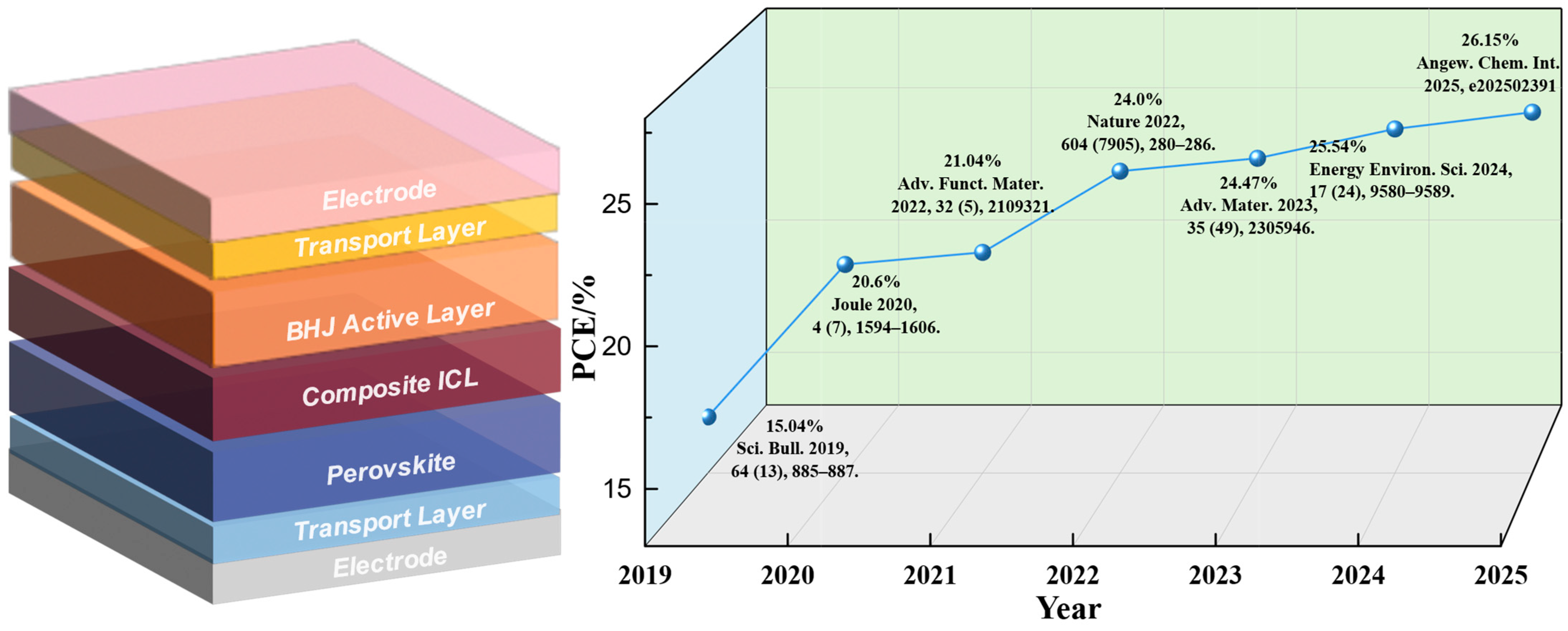
2. Architecture and Design of TSCs
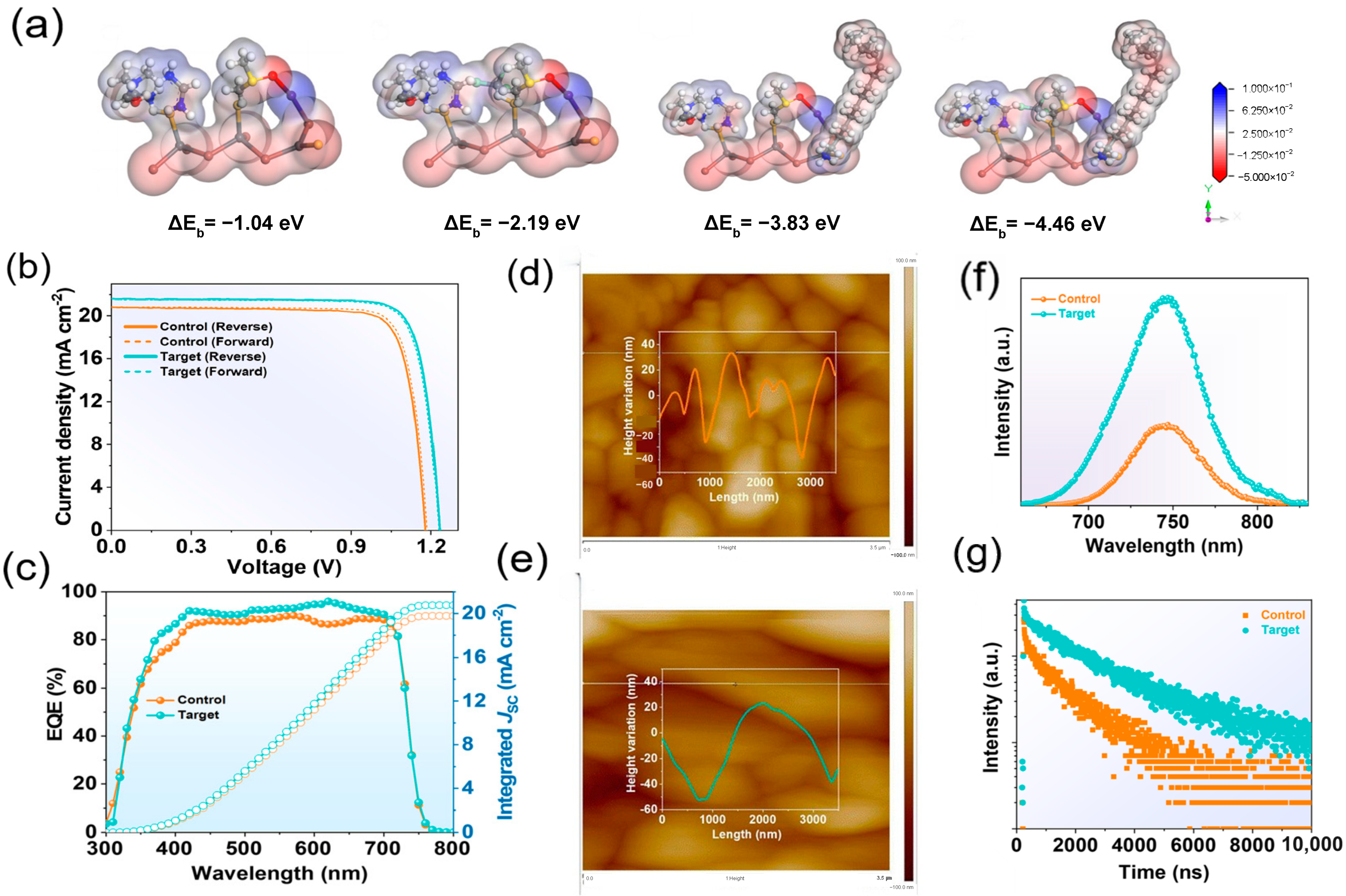
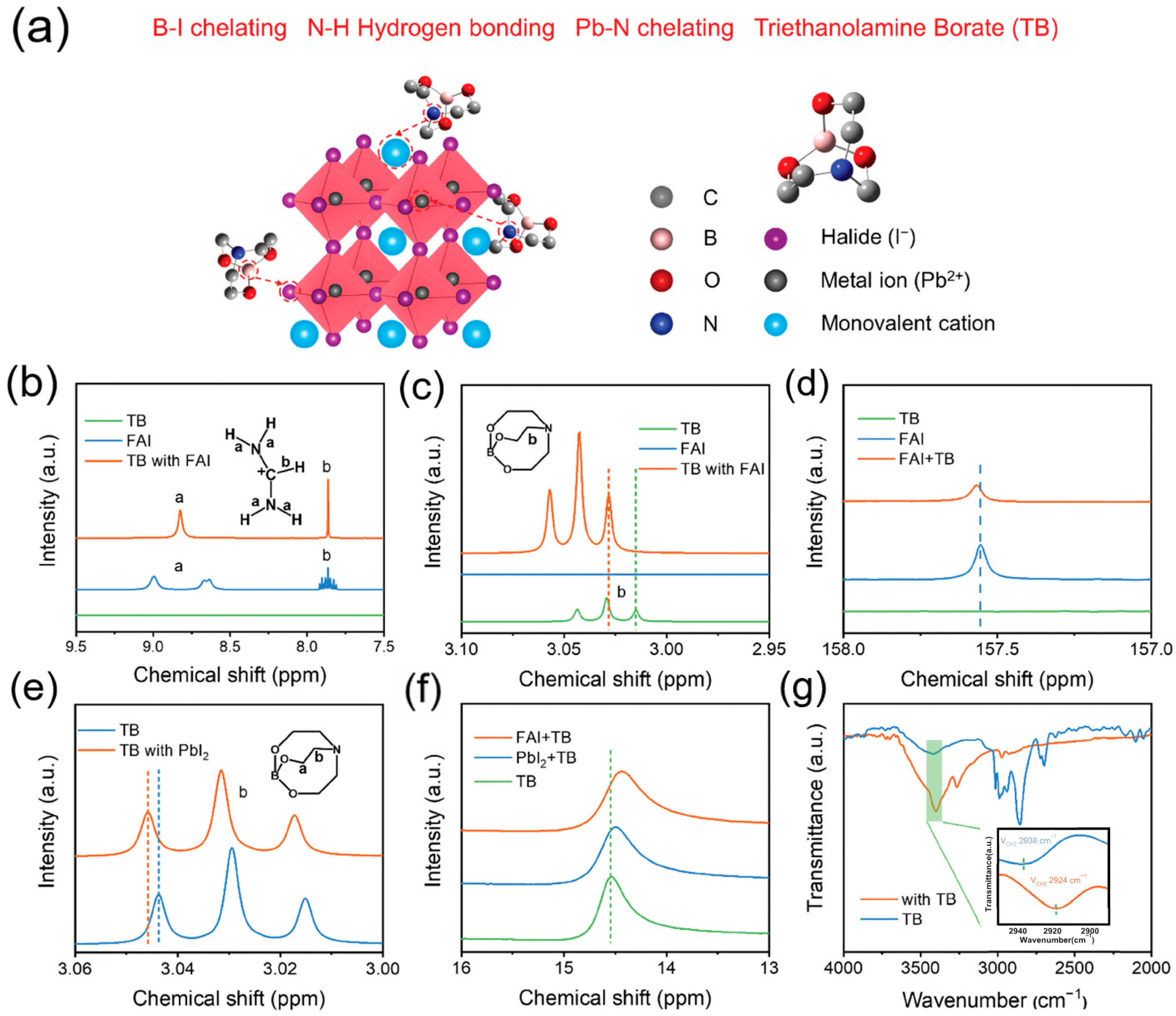
2.1. Optimization of Wide-Bandgap PSCs
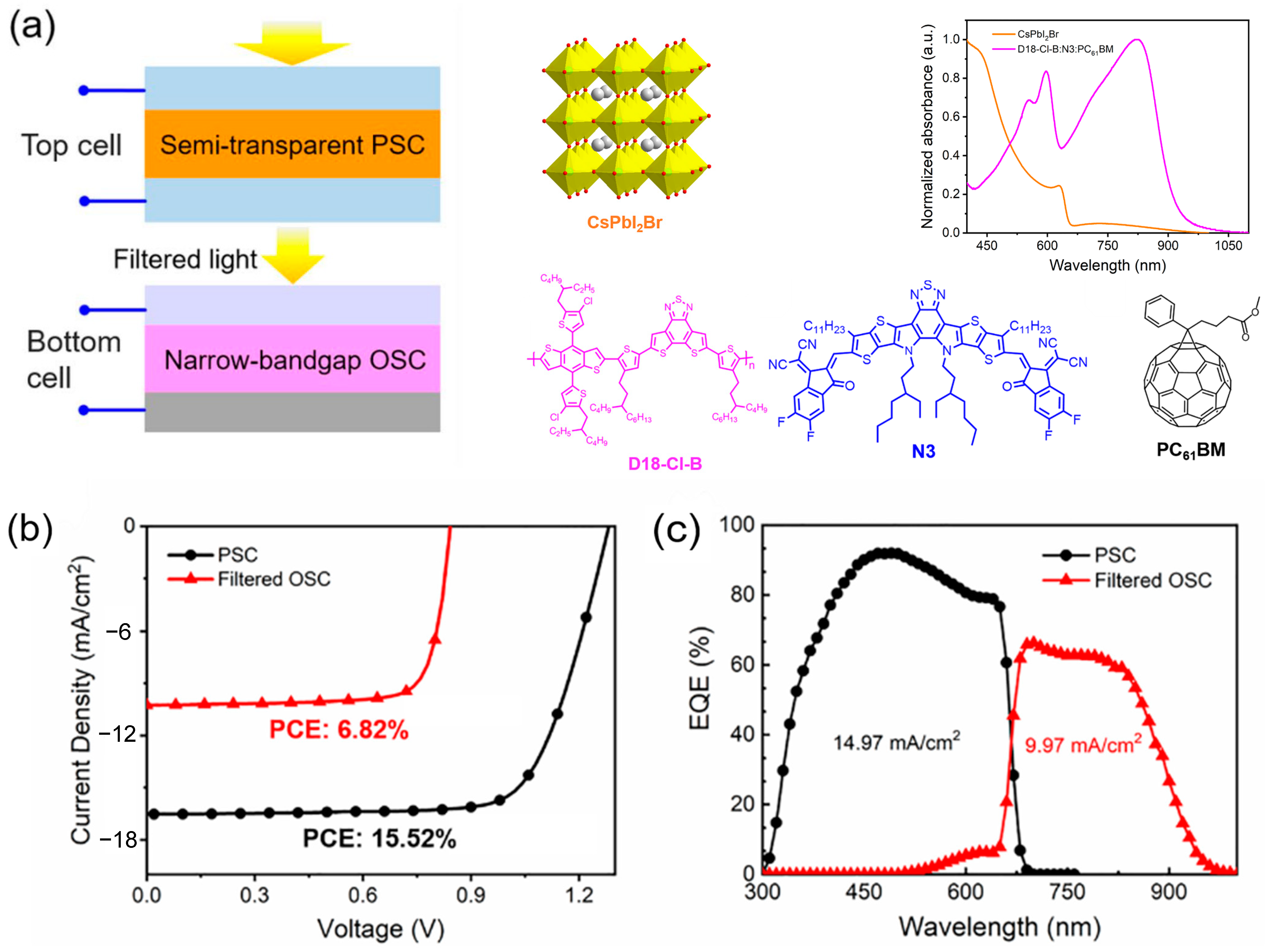
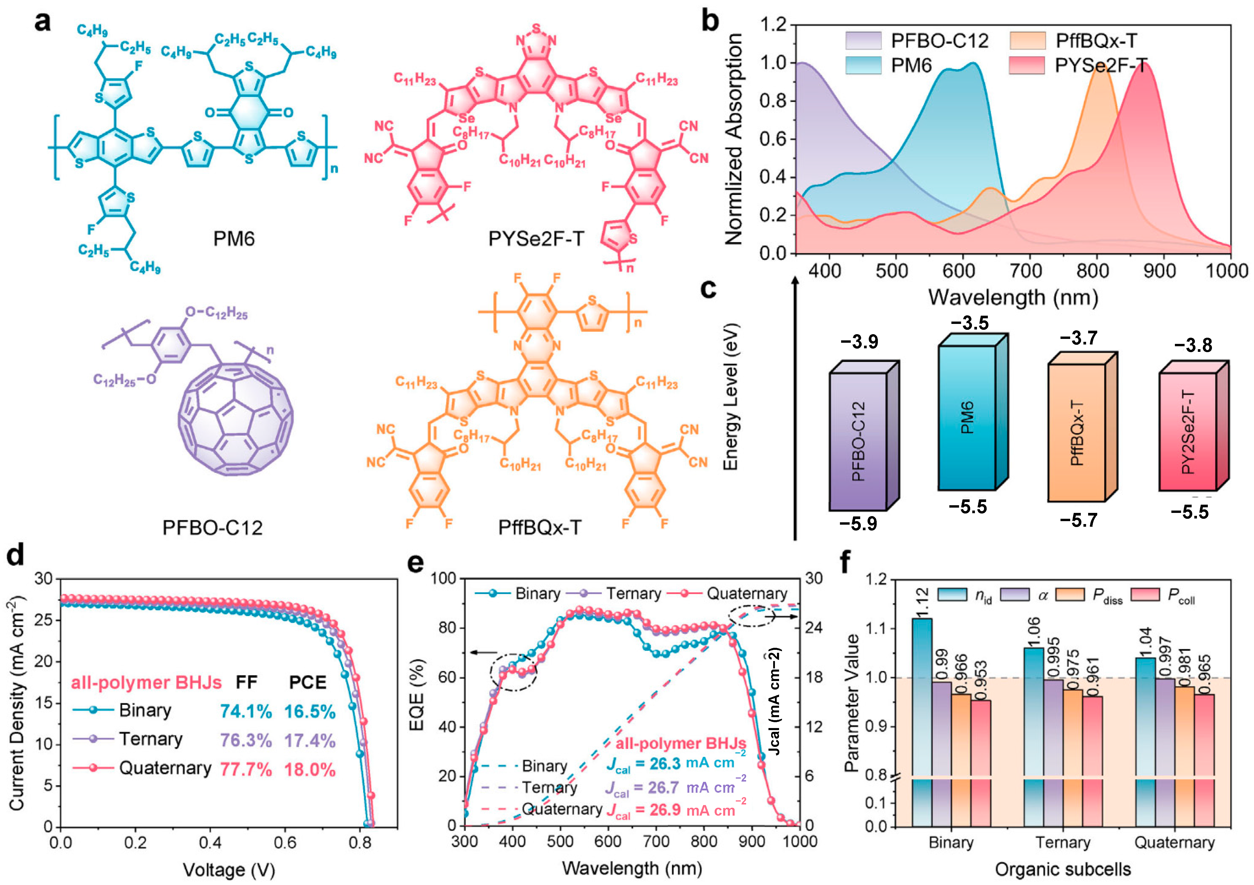
2.2. Optimization in Narrow-Bandgap OPV Sub-Cells
2.3. Design of the Interconnection Layer

| Year | Device | VOC/V | JSC/(mA cm−2) | FF/% | PCE/% | Ref |
|---|---|---|---|---|---|---|
| 2022 | ITO/NiOx/BPA/Cs0.25FA0.75Pb(I0.6Br0.4)3/C60/ BCP/IZO/MoOx/PM6:Y6/Ag | 2.06 | 14.83 | 77.2 | 23.60 | [21] |
| 2022 | ITO/MeO-2PACz/FA0.8Cs0.2Pb(I0.5Br0.5)3/PC61BM/AZO/ ALD-SnOx/InOx/MoOx/PM6:Y6/C60/BCP/Ag | 2.15 | 14.0 | 80.0 | 24.0 | [16] |
| 2023 | ITO/ZnO/SnO2/MAFm(DMSO)/CsPBI2Br/ MAFm(1-Butanol)/PDCBT/MoO3/Au/ZnO/BCP/ PM6:CH1007/MoO3/Ag | 2.10 | 14.23 | 77.70 | 23.21 | [113] |
| 2023 | ITO/MeO-2PACz/FA0.8Cs0.2Pb(I0.6Br0.4)3/C60/ C-C1-P/ITO/MoO3/PM6:BTP-eC9:PC71BM/TPMA/Ag | 2.09 | 14.58 | 78.99 | 24.07 | [106] |
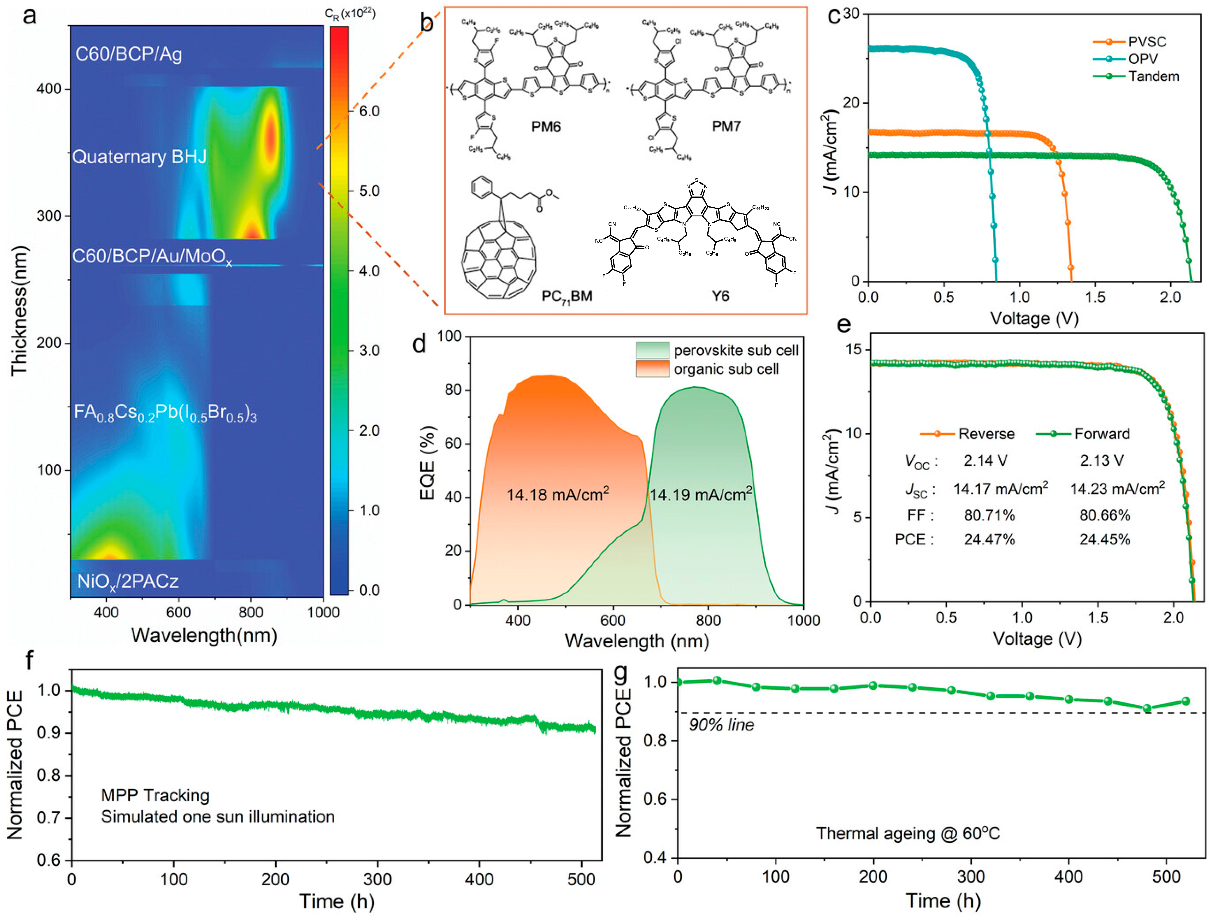
| 2023 | ITO/NiOx/2PACz/perovskite/C60/BCP/Au/MoOx/PM6:PM7:Y6:PC71BM/C60/BCP/Ag | 2.14 | 14.17 | 80.71 | 24.47 | [17] |
| 2024 | ITO/NiOx/4PADCB/FAMACsPb(I0.5Br0.5)3/PC60BM/C60/SnOx/Au/PEDOT:PSS/ D18:L8-BO:BTP-eC9-4F/PDINN/Ag | 2.20 | 13.8 | 80.6 | 24.5 | [96] |
| 2024 | ITO/NiOx/2PACz/perovskite/C60/BCP/Au/MoOx/ PM6:Y6:PC71BM/C60/BCP/Ag | 2.12 | 14.36 | 81.65 | 25.06 | [23] |
| 2024 | ITO/NiOX/Me-4PACz/perovskite/PCBM/AZO/ ITO/MoOx/PM6:BTP-eC9/PDINN/Ag | 2.144 | 14.65 | 80.02 | 25.13 | [114] |
| 2024 | ITO/DC-PA/Cs0.2FA0.8Pb(I0.6Br0.4)3/C60/BCP/Au/MoOx/ PM6:Y6:PC71BM/PNDIT-F3N/Ag | 2.151 | 14.36 | 81.65 | 25.22 | [50] |
| 2024 | ITO/CbzNaph/perovskite/C60/BCP/Au/MoOx/PM6:BTP-eC9/PDNIT-F3N/Ag | 2.15 | 14.68 | 81.03 | 25.54 | [18] |
| 2025 | m-FTO/M-SQDs/CsPbI2Br/PTQ10/MoOx/Ag/ZnO/PFN-Br/PM6:BTP-eC9/MoOx/Ag | 2.21 | 14.51 | 80.77 | 25.90 | [115] |
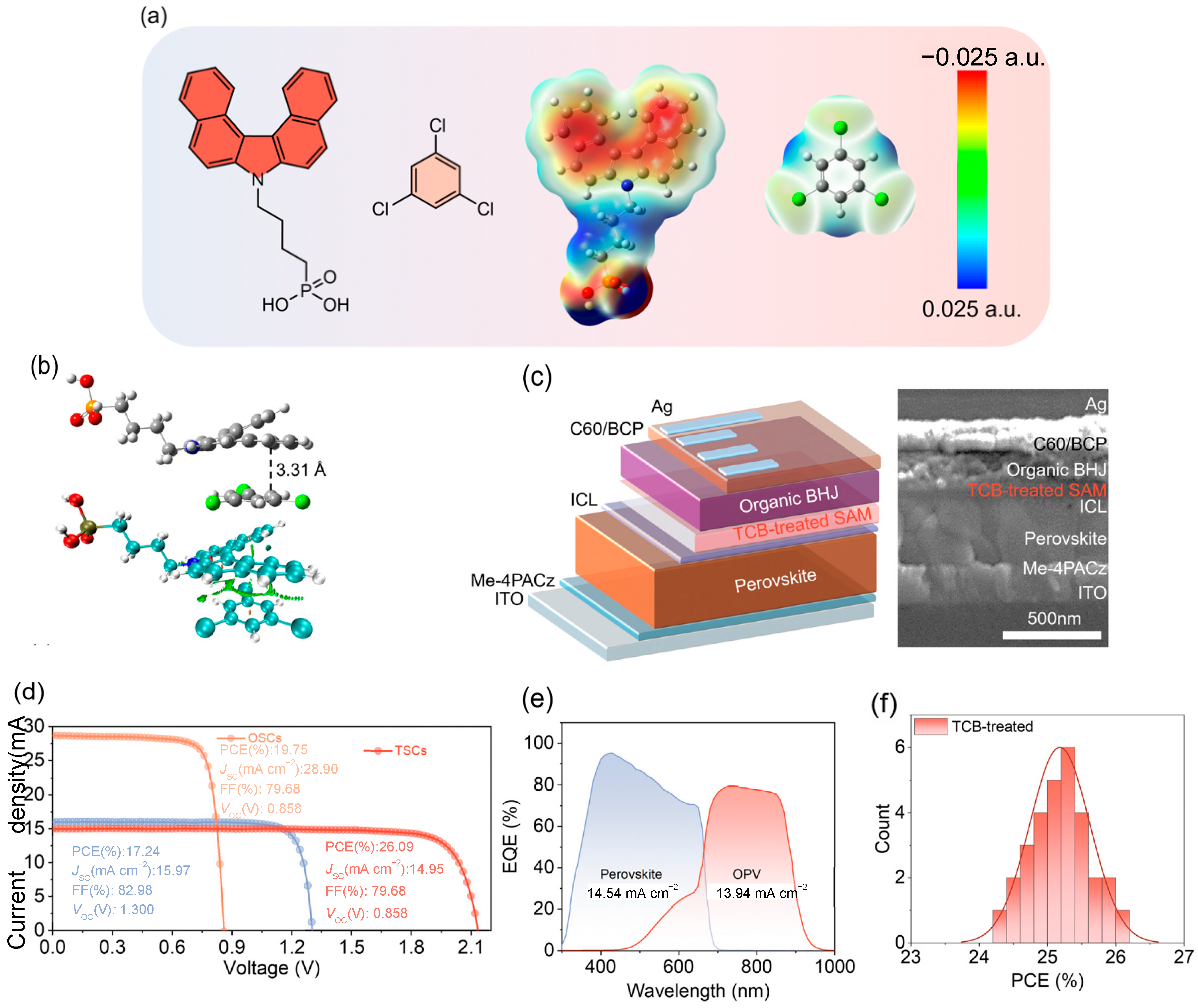
| 2025 | ITO/Me-4PACz/perovskite/C60/BCP/Ag/MoO3/ TCB-treated SAM/PM6:BTP-eC9/C60/BCP/Ag | 2.131 | 14.95 | 81.90 | 26.09 | [92] |
| 2025 | ITO/NiOx/2PACz/perovskite/C60/BCP/Ag /MoO3/2PACz/PM6:D18:BTP-eC9/C60/BCP/Ag | 2.148 | 14.60 | 83.38 | 26.15 | 19 |
3. Conclusions and Outlook
Funding
Data Availability Statement
Conflicts of Interest
References
- Wang, L.; Chen, C.; Gan, Z.; Cheng, J.; Sun, Y.; Zhou, J.; Xia, W.; Liu, D.; Li, W.; Wang, T. Diluted Ternary Heterojunctions to Suppress Charge Recombination for Organic Solar Cells with 21% Efficiency. Adv. Mater. 2025, 37, 2419923. [Google Scholar] [CrossRef]
- Shockley, W.; Queisser, H.J. Detailed Balance Limit of Efficiency of P-n Junction Solar Cells. J. Appl. Phys. 1961, 32, 510–519. [Google Scholar] [CrossRef]
- Rühle, S. Tabulated Values of the Shockley–Queisser Limit for Single Junction Solar Cells. Sol. Energy 2016, 130, 139–147. [Google Scholar] [CrossRef]
- Kirchartz, T.; Rau, U. What Makes a Good Solar Cell? Adv. Energy Mater. 2018, 8, 1703385. [Google Scholar] [CrossRef]
- Weber, D. CH3 NH3 PbX3, Ein Pb(II)-System Mit Kubischer Perowskitstruktur/CH3 NH3 PbX3, a Pb(II)-System with Cubic Perovskite Structure. Z. Naturforschung B 1978, 33, 1443–1445. [Google Scholar] [CrossRef]
- Eperon, G.E.; Leijtens, T.; Bush, K.A.; Prasanna, R.; Green, T.; Wang, J.T.-W.; McMeekin, D.P.; Volonakis, G.; Milot, R.L.; May, R.; et al. Perovskite-Perovskite Tandem Photovoltaics with Optimized Bandgaps. Science 2016, 354, 861–865. [Google Scholar] [CrossRef] [PubMed]
- Eperon, G.E.; Stranks, S.D.; Menelaou, C.; Johnston, M.B.; Herz, L.M.; Snaith, H.J. Formamidinium Lead Trihalide: A Broadly Tunable Perovskite for Efficient Planar Heterojunction Solar Cells. Energy Environ. Sci. 2014, 7, 982. [Google Scholar] [CrossRef]
- Unger, E.L.; Kegelmann, L.; Suchan, K.; Sörell, D.; Korte, L.; Albrecht, S. Roadmap and Roadblocks for the Band Gap Tunability of Metal Halide Perovskites. J. Mater. Chem. A 2017, 5, 11401–11409. [Google Scholar] [CrossRef]
- Khan, F.; Rezgui, B.D.; Khan, M.T.; Al-Sulaiman, F. Perovskite-Based Tandem Solar Cells: Device Architecture, Stability, and Economic Perspectives. Renew. Sustain. Energy Rev. 2022, 165, 112553–112574. [Google Scholar] [CrossRef]
- Ho, C.H.Y.; Kim, T.; Xiong, Y.; Firdaus, Y.; Yi, X.; Dong, Q.; Rech, J.J.; Gadisa, A.; Booth, R.; O’Connor, B.T.; et al. High-Performance Tandem Organic Solar Cells Using HSolar as the Interconnecting Layer. Adv. Energy Mater. 2020, 10, 2000823. [Google Scholar] [CrossRef]
- Wang, R.; Huang, T.; Xue, J.; Tong, J.; Zhu, K.; Yang, Y. Prospects for Metal Halide Perovskite-Based Tandem Solar Cells. Nat. Photonics 2021, 15, 411–425. [Google Scholar] [CrossRef]
- Xu, Q.; Zhao, Y.; Zhang, X. Light Management in Monolithic Perovskite/Silicon Tandem Solar Cells. Sol. RRL 2020, 4, 1900206. [Google Scholar] [CrossRef]
- Zeng, Q.; Liu, L.; Xiao, Z.; Liu, F.; Hua, Y.; Yuan, Y.; Ding, L. A Two-Terminal All-Inorganic Perovskite/Organic Tandem Solar Cell. Sci. Bull. 2019, 64, 885–887. [Google Scholar] [CrossRef]
- Chen, X.; Jia, Z.; Chen, Z.; Jiang, T.; Bai, L.; Tao, F.; Chen, J.; Chen, X.; Liu, T.; Xu, X.; et al. Efficient and Reproducible Monolithic Perovskite/Organic Tandem Solar Cells with Low-Loss Interconnecting Layers. Joule 2020, 4, 1594–1606. [Google Scholar] [CrossRef]
- Chen, W.; Li, D.; Chen, X.; Chen, H.; Liu, S.; Yang, H.; Li, X.; Shen, Y.; Ou, X.; Yang, Y.; et al. Surface Reconstruction for Stable Monolithic All-inorganic Perovskite/Organic Tandem Solar Cells with over 21% Efficiency. Adv. Funct. Mater. 2022, 32, 2109321. [Google Scholar] [CrossRef]
- Brinkmann, K.O.; Becker, T.; Zimmermann, F.; Kreusel, C.; Gahlmann, T.; Theisen, M.; Haeger, T.; Olthof, S.; Tückmantel, C.; Günster, M.; et al. Perovskite–Organic Tandem Solar Cells with Indium Oxide Interconnect. Nature 2022, 604, 280–286. [Google Scholar] [CrossRef] [PubMed]
- Wang, X.; Zhang, D.; Liu, B.; Wu, X.; Jiang, X.; Zhang, S.; Wang, Y.; Gao, D.; Wang, L.; Wang, H.; et al. Highly Efficient Perovskite/Organic Tandem Solar Cells Enabled by Mixed-cation Surface Modulation. Adv. Mater. 2023, 35, 2305946. [Google Scholar] [CrossRef] [PubMed]
- Chen, M.; Li, Y.; Zeng, Z.; Liu, M.; Du, T.; Huang, X.; Bi, L.; Wang, J.; Jiang, W.; An, Y.; et al. Regulating the Crystallization of Mixed-Halide Perovskites by Cation Alloying for Perovskite–Organic Tandem Solar Cells. Energy Environ. Sci. 2024, 17, 9580–9589. [Google Scholar] [CrossRef]
- Dong, P.; Zhang, Z.; Chen, W.; Zheng, J.; Xu, J.; Wang, Z.; Kang, S.; Chen, H.; Jiang, X.; Cao, J.; et al. Retarding Phase Segregation via Lattice Reinforcement for Efficient and Stable Perovskite/Organic Tandems. Angew. Chem. 2025, 137, e202502391. [Google Scholar] [CrossRef]
- Chen, C.-C.; Bae, S.-H.; Chang, W.-H.; Hong, Z.; Li, G.; Chen, Q.; Zhou, H.; Yang, Y. Perovskite/Polymer Monolithic Hybrid Tandem Solar Cells Utilizing a Low-Temperature, Full Solution Process. Mater. Horiz. 2015, 2, 203–211. [Google Scholar] [CrossRef]
- Chen, W.; Zhu, Y.; Xiu, J.; Chen, G.; Liang, H.; Liu, S.; Xue, H.; Birgersson, E.; Ho, J.W.; Qin, X.; et al. Monolithic Perovskite/Organic Tandem Solar Cells with 23.6% Efficiency Enabled by Reduced Voltage Losses and Optimized Interconnecting Layer. Nat. Energy 2022, 7, 229–237. [Google Scholar] [CrossRef]
- Brinkmann, K.O.; Wang, P.; Lang, F.; Li, W.; Guo, X.; Zimmermann, F.; Olthof, S.; Neher, D.; Hou, Y.; Stolterfoht, M.; et al. Perovskite–Organic Tandem Solar Cells. Nat. Rev. Mater. 2024, 9, 202–217. [Google Scholar] [CrossRef]
- Zhang, Z.; Chen, W.; Jiang, X.; Cao, J.; Yang, H.; Chen, H.; Yang, F.; Shen, Y.; Yang, H.; Cheng, Q.; et al. Suppression of Phase Segregation in Wide-Bandgap Perovskites with Thiocyanate Ions for Perovskite/Organic Tandems with 25.06% Efficiency. Nat. Energy 2024, 9, 592–601. [Google Scholar] [CrossRef]
- Jiang, S.; Wang, R.; Li, M.; Yu, R.; Wang, F.; Tan, Z. Synergistic Electrical and Light Management Enables Efficient Monolithic Inorganic Perovskite/Organic Tandem Solar Cells with over 24% Efficiency. Energy Environ. Sci. 2024, 17, 219–226. [Google Scholar] [CrossRef]
- Bai, Y.; Han, F.; Zeng, R.; Tian, S.; Wang, F.; Wang, X.; Dai, M.; Li, M.; Tan, Z. Synergy of the Transmittance Fluctuation Factor and Absorption Selectivity for Efficient Semitransparent Perovskite/Organic Tandem Solar Cells with High Color-Fidelity. J. Mater. Chem. A 2023, 11, 17514–17524. [Google Scholar] [CrossRef]
- Wang, P.; Li, W.; Sandberg, O.J.; Guo, C.; Sun, R.; Wang, H.; Li, D.; Zhang, H.; Cheng, S.; Liu, D.; et al. Tuning of the Interconnecting Layer for Monolithic Perovskite/Organic Tandem Solar Cells with Record Efficiency Exceeding 21%. Nano Lett. 2021, 21, 7845–7854. [Google Scholar] [CrossRef]
- García Cerrillo, J.; Distler, A.; Matteocci, F.; Forberich, K.; Wagner, M.; Basu, R.; Castriotta, L.A.; Jafarzadeh, F.; Brunetti, F.; Yang, F.; et al. Matching the Photocurrent of 2-terminal Mechanically-stacked Perovskite/Organic Tandem Solar Modules by Varying the Cell Width. Sol. RRL 2024, 8, 2300767. [Google Scholar] [CrossRef]
- Warren, E.L.; McMahon, W.E.; Rienäcker, M.; VanSant, K.T.; Whitehead, R.C.; Peibst, R.; Tamboli, A.C. A Taxonomy for Three-Terminal Tandem Solar Cells. ACS Energy Lett. 2020, 5, 1233–1242. [Google Scholar] [CrossRef]
- Yang, Y.; Chen, Q.; Hsieh, Y.-T.; Song, T.-B.; Marco, N.D.; Zhou, H.; Yang, Y. Multilayer Transparent Top Electrode for Solution Processed Perovskite/Cu(In,Ga)(Se,S)2 Four Terminal Tandem Solar Cells. ACS Nano 2015, 9, 7714–7721. [Google Scholar] [CrossRef]
- Zhao, D.; Wang, C.; Song, Z.; Yu, Y.; Chen, C.; Zhao, X.; Zhu, K.; Yan, Y. Four-Terminal All-Perovskite Tandem Solar Cells Achieving Power Conversion Efficiencies Exceeding 23%. ACS Energy Lett. 2018, 3, 305–306. [Google Scholar] [CrossRef]
- Guchhait, A.; Dewi, H.A.; Leow, S.W.; Wang, H.; Han, G.; Suhaimi, F.B.; Mhaisalkar, S.; Wong, L.H.; Mathews, N. Over 20% Efficient CIGS–Perovskite Tandem Solar Cells. ACS Energy Lett. 2017, 2, 807–812. [Google Scholar] [CrossRef]
- Zhao, D.; Yu, Y.; Wang, C.; Liao, W.; Shrestha, N.; Grice, C.R.; Cimaroli, A.J.; Guan, L.; Ellingson, R.J.; Zhu, K.; et al. Low-Bandgap Mixed Tin–Lead Iodide Perovskite Absorbers with Long Carrier Lifetimes for All-Perovskite Tandem Solar Cells. Nat. Energy 2017, 2, 17018. [Google Scholar] [CrossRef]
- Liu, L.; Xiao, H.; Jin, K.; Xiao, Z.; Du, X.; Yan, K.; Hao, F.; Bao, Q.; Yi, C.; Liu, F.; et al. 4-Terminal Inorganic Perovskite/Organic Tandem Solar Cells Offer 22% Efficiency. Nano Micro Lett. 2023, 15, 23–33. [Google Scholar] [CrossRef] [PubMed]
- Tong, J.; Jiang, Q.; Zhang, F.; Kang, S.B.; Kim, D.H.; Zhu, K. Wide-Bandgap Metal Halide Perovskites for Tandem Solar Cells. ACS Energy Lett. 2021, 6, 232–248. [Google Scholar] [CrossRef] [PubMed]
- Wang, R.; Li, M.; Ma, Z.; He, Z.; Dong, Y.; Zhang, Y.; Xu, Z.; Su, G.; Tan, Z. Hexachlorotriphosphazene-Assisted Buried Interface Passivation for Stable and Efficient Wide-Bandgap Perovskite Solar Cells. Chem. Commun. 2023, 59, 6255–6258. [Google Scholar] [CrossRef]
- Leijtens, T.; Bush, K.A.; Prasanna, R.; McGehee, M.D. Opportunities and Challenges for Tandem Solar Cells Using Metal Halide Perovskite Semiconductors. Nat. Energy 2018, 3, 828–838. [Google Scholar] [CrossRef]
- Qin, S.; Lu, C.; Jia, Z.; Wang, Y.; Li, S.; Lai, W.; Shi, P.; Wang, R.; Zhu, C.; Du, J.; et al. Constructing Monolithic Perovskite/Organic Tandem Solar Cell with Efficiency of 22.0% via Reduced Open-Circuit Voltage Loss and Broadened Absorption Spectra. Adv. Mater. 2022, 34, 2108829. [Google Scholar] [CrossRef]
- He, R.; Ren, S.; Chen, C.; Yi, Z.; Luo, Y.; Lai, H.; Wang, W.; Zeng, G.; Hao, X.; Wang, Y.; et al. Wide-Bandgap Organic–Inorganic Hybrid and All-Inorganic Perovskite Solar Cells and Their Application in All-Perovskite Tandem Solar Cells. Energy Environ. Sci. 2021, 14, 5723–5759. [Google Scholar] [CrossRef]
- Mahesh, S.; Ball, J.M.; Oliver, R.D.J.; McMeekin, D.P.; Nayak, P.K.; Johnston, M.B.; Snaith, H.J. Revealing the Origin of Voltage Loss in Mixed-Halide Perovskite Solar Cells. Energy Environ. Sci. 2020, 13, 258–267. [Google Scholar] [CrossRef]
- Mahmud, M.A.; Zheng, J.; Chang, J.; Wang, G.; Liao, C.; Rahman, M.H.; Tarique, W.B.; Tang, S.; Bing, J.; Bailey, C.G.; et al. Halogenated Polycyclic Aromatic Hydrocarbon for Hole Selective Layer/Perovskite Interface Modification and Passivation for Efficient Perovskite-Organic Tandem Solar Cells with Record Fill Factor. Adv. Energy Mater. 2024, 14, 2400691. [Google Scholar] [CrossRef]
- Aslam, F.; Li, H.; Yang, F.; Feng, E.; Chang, J.; Ding, Y.; Liao, X.; Zahid, M.; Sadiq, M.I.; Tahir, M.; et al. Precise Control on the Crystallization with Co-Anti-Solvents in Wide-Bandgap Perovskite Film for Efficient Perovskite-Organic Tandem Solar Cells. J. Cent. South Univ. 2024, 31, 4328–4337. [Google Scholar] [CrossRef]
- Mali, S.S.; Patil, J.V.; Steele, J.A.; Nazeeruddin, M.K.; Kim, J.H.; Hong, C.K. All-Inorganic Halide Perovskites for Air-Processed “n–i–p” Monolithic Perovskite/Organic Hybrid Tandem Solar Cells Exceeding 23% Efficiency. Energy Environ. Sci. 2024, 17, 1046–1060. [Google Scholar] [CrossRef]
- Abdollahi Nejand, B.; Ritzer, D.B.; Hu, H.; Schackmar, F.; Moghadamzadeh, S.; Feeney, T.; Singh, R.; Laufer, F.; Schmager, R.; Azmi, R.; et al. Scalable Two-Terminal All-Perovskite Tandem Solar Modules with a 19.1% Efficiency. Nat. Energy 2022, 7, 620–630. [Google Scholar] [CrossRef]
- Ma, Q.; Wang, Y.; Liu, L.; Yang, P.; He, W.; Zhang, X.; Zheng, J.; Ma, M.; Wan, M.; Yang, Y.; et al. One-Step Dual-Additive Passivated Wide-Bandgap Perovskites to Realize 44.72%-Efficient Indoor Photovoltaics. Energy Environ. Sci. 2024, 17, 1637–1644. [Google Scholar] [CrossRef]
- Li, J.; Zhu, S.; Yin, C.; Chen, C.; Yuan, J.; Zhao, H.; Gong, H.; Yang, B.; Zheng, D.; Xing, G.; et al. Homogenizing the Halogen Distribution via a Multifunctional Fluorine-Containing Additive toward High-performance Inverted Wide-bandgap Perovskite Solar Cells. Adv. Funct. Mater. 2025, 2422175. [Google Scholar] [CrossRef]
- Chen, H.; Sun, J.; Fan, K.; Zou, S.; Lin, Z.; Chen, J.; Zhang, Z.; Wang, K.; Jiang, Z.; Yan, K. Difunctional Polymerizable Additive Enables Efficient and Stable Wide-Bandgap Perovskites for Perovskite/Organic Tandems Solar Cells. Adv. Funct. Mater. 2025, 2502422. [Google Scholar] [CrossRef]
- Yu, X.; Wang, Y.; Gao, P. The Effect of Redox Reactions on the Stability of Perovskite Solar Cells. Chemphotochem 2023, 7, e202200311. [Google Scholar] [CrossRef]
- Kim, D.; Jung, H.J.; Park, I.J.; Larson, B.W.; Dunfield, S.P.; Xiao, C.; Kim, J.; Tong, J.; Boonmongkolras, P.; Ji, S.G.; et al. Efficient, Stable Silicon Tandem Cells Enabled by Anion-Engineered Wide-Bandgap Perovskites. Science 2020, 368, 155–160. [Google Scholar] [CrossRef]
- Duong, T.; Pham, H.; Yin, Y.; Peng, J.; Mahmud, M.A.; Wu, Y.; Shen, H.; Zheng, J.; Tran-Phu, T.; Lu, T.; et al. Efficient and Stable Wide Bandgap Perovskite Solar Cells Through Surface Passivation with Long Alkyl Chain Organic Cations. J. Mater. Chem. A 2021, 9, 18454–18465. [Google Scholar] [CrossRef]
- Wu, S.; Yan, Y.; Yin, J.; Jiang, K.; Li, F.; Zeng, Z.; Tsang, S.-W.; Jen, A.K.-Y. Redox Mediator-Stabilized Wide-Bandgap Perovskites for Monolithic Perovskite-Organic Tandem Solar Cells. Nat. Energy 2024, 9, 411–421. [Google Scholar] [CrossRef]
- An, Y.; Zhang, N.; Zeng, Z.; Cai, Y.; Jiang, W.; Qi, F.; Ke, L.; Lin, F.R.; Tsang, S.; Shi, T.; et al. Optimizing Crystallization in Wide-bandgap Mixed Halide Perovskites for High-Efficiency Solar Cells. Adv. Mater. 2024, 36, 2306568. [Google Scholar] [CrossRef] [PubMed]
- Su, G.; Yu, R.; Dong, Y.; He, Z.; Zhang, Y.; Wang, R.; Dang, Q.; Sha, S.; Lv, Q.; Xu, Z.; et al. Crystallization Regulation and Defect Passivation for Efficient Inverted Wide-Bandgap Perovskite Solar Cells with over 21% Efficiency. Adv. Energy Mater. 2024, 14, 2303344. [Google Scholar] [CrossRef]
- Xie, Y.; Yao, Q.; Zeng, Z.; Xue, Q.; Niu, T.; Xia, R.; Cheng, Y.; Lin, F.; Tsang, S.; Jen, A.K.-Y.; et al. Homogeneous Grain Boundary Passivation in Wide-Bandgap Perovskite Films Enables Fabrication of Monolithic Perovskite/Organic Tandem Solar Cells with over 21% Efficiency. Adv. Funct. Mater. 2022, 32, 2112126. [Google Scholar] [CrossRef]
- Lv, X.; Li, W.; Zhang, J.; Yang, Y.; Jia, X.; Ji, Y.; Lin, Q.; Huang, W.; Bu, T.; Ren, Z.; et al. Surface Repair of Wide-Bandgap Perovskites for High-Performance All-Perovskite Tandem Solar Cells. J. Energy Chem. 2024, 93, 64–70. [Google Scholar] [CrossRef]
- Jiang, X.; Qin, S.; Meng, L.; He, G.; Zhang, J.; Wang, Y.; Zhu, Y.; Zou, T.; Gong, Y.; Chen, Z.; et al. Isomeric Diammonium Passivation for Perovskite–Organic Tandem Solar Cells. Nature 2024, 635, 860–866. [Google Scholar] [CrossRef]
- Wang, Y.; Yu, J.; Zhang, R.; Yuan, J.; Hultmark, S.; Johnson, C.E.; Gallop, N.P.; Siegmund, B.; Qian, D.; Zhang, H.; et al. Origins of the Open-Circuit Voltage in Ternary Organic Solar Cells and Design Rules for Minimized Voltage Losses. Nat. Energy 2023, 8, 978–988. [Google Scholar] [CrossRef]
- Wu, J.; Ling, Z.; Franco, L.R.; Jeong, S.Y.; Genene, Z.; Mena, J.; Chen, S.; Chen, C.; Araujo, C.M.; Marchiori, C.F.N.; et al. On the Conformation of Dimeric Acceptors and Their Polymer Solar Cells with Efficiency over 18%. Angew. Chem. 2023, 135, e202302888. [Google Scholar] [CrossRef]
- Sun, B.; Tokmoldin, N.; Alqahtani, O.; Patterson, A.; De Castro, C.S.P.; Riley, D.B.; Pranav, M.; Armin, A.; Laquai, F.; Collins, B.A.; et al. Toward More Efficient Organic Solar Cells: A Detailed Study of Loss Pathway and Its Impact on Overall Device Performance in Low-Offset Organic Solar Cells. Adv. Energy Mater. 2023, 13, 2300980. [Google Scholar] [CrossRef]
- Zhang, S.; Qin, Y.; Zhu, J.; Hou, J. Over 14% Efficiency in Polymer Solar Cells Enabled by a Chlorinated Polymer Donor. Adv. Mater. 2018, 30, 1800868. [Google Scholar] [CrossRef]
- Qian, D.; Ye, L.; Zhang, M.; Liang, Y.; Li, L.; Huang, Y.; Guo, X.; Zhang, S.; Tan, Z.; Hou, J. Design, Application, and Morphology Study of a New Photovoltaic Polymer with Strong Aggregation in Solution State. Macromolecules 2012, 45, 9611–9617. [Google Scholar] [CrossRef]
- Zhang, M.; Guo, X.; Ma, W.; Ade, H.; Hou, J. A Large-Bandgap Conjugated Polymer for Versatile Photovoltaic Applications with High Performance. Adv. Mater. 2015, 27, 4655–4660. [Google Scholar] [CrossRef]
- Xin, Y.; Liu, H.; Dong, X.; Xiao, Z.; Wang, R.; Gao, Y.; Zou, Y.; Kan, B.; Wan, X.; Liu, Y.; et al. Multiarmed Aromatic Ammonium Salts Boost the Efficiency and Stability of Inverted Organic Solar Cells. J. Am. Chem. Soc. 2024, 146, 3363–3372. [Google Scholar] [CrossRef]
- Chen, H.; Kan, B.; Wang, P.; Feng, W.; Li, L.; Zhang, S.; Chen, T.; Yang, Y.; Duan, T.; Yao, Z.; et al. Terminally Chlorinated and Thiophene-Linked Acceptor-Donor-Acceptor Structured 3D Acceptors with Versatile Processability for High-Efficiency Organic Solar Cells. Angew. Chem. Int. Ed. 2023, 62, e202307962. [Google Scholar] [CrossRef] [PubMed]
- Zhang, G.; Lin, F.R.; Qi, F.; Heumüller, T.; Distler, A.; Egelhaaf, H.-J.; Li, N.; Chow, P.C.Y.; Brabec, C.J.; Jen, A.K.-Y.; et al. Renewed Prospects for Organic Photovoltaics. Chem. Rev. 2022, 122, 14180–14274. [Google Scholar] [CrossRef] [PubMed]
- Gurney, R.S.; Lidzey, D.G.; Wang, T. A Review of Non-Fullerene Polymer Solar Cells: From Device Physics to Morphology Control. Rep. Prog. Phys. 2019, 82, 36601. [Google Scholar] [CrossRef]
- Yuan, J.; Huang, T.; Cheng, P.; Zou, Y.; Zhang, H.; Yang, J.L.; Chang, S.-Y.; Zhang, Z.; Huang, W.; Wang, R.; et al. Enabling Low Voltage Losses and High Photocurrent in Fullerene-Free Organic Photovoltaics. Nat. Commun. 2019, 10, 570. [Google Scholar] [CrossRef] [PubMed]
- Wang, J.; Xue, P.; Jiang, Y.; Huo, Y.; Zhan, X. The Principles, Design and Applications of Fused-Ring Electron Acceptors. Nat. Rev. Chem. 2022, 6, 614–634. [Google Scholar] [CrossRef]
- Li, C.; Zhou, J.; Song, J.; Xu, J.; Zhang, H.; Zhang, X.; Guo, J.; Zhu, L.; Wei, D.; Han, G.; et al. Non-Fullerene Acceptors with Branched Side Chains and Improved Molecular Packing to Exceed 18% Efficiency in Organic Solar Cells. Nat. Energy 2021, 6, 605–613. [Google Scholar] [CrossRef]
- Salem, M.S.; Shaker, A.; Abouelatta, M.; Saeed, A. Full Optoelectronic Simulation of Lead-Free Perovskite/Organic Tandem Solar Cells. Polymers 2023, 15, 784. [Google Scholar] [CrossRef]
- Li, G.; Zhang, X.; Jones, L.O.; Alzola, J.M.; Mukherjee, S.; Feng, L.; Zhu, W.; Stern, C.L.; Huang, W.; Yu, J.; et al. Systematic Merging of Nonfullerene Acceptor π-Extension and Tetrafluorination Strategies Affords Polymer Solar Cells with >16% Efficiency. J. Am. Chem. Soc. 2021, 143, 6123–6139. [Google Scholar] [CrossRef]
- Zhang, G.; Chen, X.-K.; Xiao, J.; Chow, P.C.Y.; Ren, M.; Kupgan, G.; Jiao, X.; Chan, C.C.S.; Du, X.; Xia, R.; et al. Delocalization of Exciton and Electron Wavefunction in Non-Fullerene Acceptor Molecules Enables Efficient Organic Solar Cells. Nat. Commun. 2020, 11, 3943. [Google Scholar] [CrossRef] [PubMed]
- Liu, K.; Jiang, Y.; Ran, G.; Liu, F.; Zhang, W.; Zhu, X. 19.7% Efficiency Binary Organic Solar Cells Achieved by Selective Core Fluorination of Nonfullerene Electron Acceptors. Joule 2024, 8, 835–851. [Google Scholar] [CrossRef]
- Liu, K.; Jiang, Y.; Liu, F.; Zhu, X. Quinoxaline-Based Nonfullerene Acceptors with Powerful Core-Functionalization Ability Enabling Efficient Solar Energy Utilization. Energy Environ. Sci. 2024, 17, 4944–4967. [Google Scholar] [CrossRef]
- Liu, H.; Geng, Y.; Xiao, Z.; Ding, L.; Du, J.; Tang, A.; Zhou, E. The Development of Quinoxaline-Based Electron Acceptors for High Performance Organic Solar Cells. Adv. Mater. 2024, 36, 2404660. [Google Scholar] [CrossRef] [PubMed]
- Yuan, J.; Zhang, Y.; Zhou, L.; Zhang, G.; Yip, H.-L.; Lau, T.-K.; Lu, X.; Zhu, C.; Peng, H.; Johnson, P.A.; et al. Single-Junction Organic Solar Cell with over 15% Efficiency Using Fused-Ring Acceptor with Electron-Deficient Core. Joule 2019, 3, 1140–1151. [Google Scholar] [CrossRef]
- Cheng, Y.-J.; Chen, C.-H.; Ho, Y.-J.; Chang, S.-W.; Witek, H.A.; Hsu, C.-S. Thieno[3,2-b]Pyrrolo Donor Fused with Benzothiadiazolo, Benzoselenadiazolo and Quinoxalino Acceptors: Synthesis, Characterization, and Molecular Properties. Org. Lett. 2011, 13, 5484–5487. [Google Scholar] [CrossRef]
- Feng, L.; Yuan, J.; Zhang, Z.; Peng, H.; Zhang, Z.-G.; Xu, S.; Liu, Y.; Li, Y.; Zou, Y. Thieno[3,2-b]Pyrrolo-Fused Pentacyclic Benzotriazole-Based Acceptor for Efficient Organic Photovoltaics. ACS Appl. Mater. Interfaces 2017, 9, 31985–31992. [Google Scholar] [CrossRef]
- Yuan, J.; Zhang, C.; Chen, H.; Zhu, C.; Cheung, S.H.; Qiu, B.; Cai, F.; Wei, Q.; Liu, W.; Yin, H.; et al. Understanding Energetic Disorder in Electron-Deficient-Core-Based Non-Fullerene Solar Cells. Sci. China Chem. 2020, 63, 1159–1168. [Google Scholar] [CrossRef]
- Yue, Q.; Liu, W.; Zhu, X. N-Type Molecular Photovoltaic Materials: Design Strategies and Device Applications. J. Am. Chem. Soc. 2020, 142, 11613–11628. [Google Scholar] [CrossRef]
- Liu, W.; Duan, Y.; Zhang, Z.; Gao, J.; Li, S.; Fink, Z.; Wu, X.; Ma, Z.; Saeki, A.; Russell, T.P.; et al. Rational Organic Subcell Engineering Enables Efficient Organic-Perovskite Tandem Solar Cells. ACS Energy Lett. 2023, 8, 4514–4523. [Google Scholar] [CrossRef]
- Jacobs, I.E. Photoinduced Degradation from Trace 1,8-Diiodooctane in Organic Photovoltaics. J. Mater. Chem. C 2018, 6, 219–225. [Google Scholar] [CrossRef]
- He, X.; Chan, C.C.S.; Kim, J.; Liu, H.; Su, C.-J.; Jeng, U.-S.; Su, H.; Lu, X.; Wong, K.S.; Choy, W.C.H. 1-Chloronaphthalene-Induced Donor/Acceptor Vertical Distribution and Carrier Dynamics Changes in Nonfullerene Organic Solar Cells and the Governed Mechanism. Small Methods 2022, 6, 2101475. [Google Scholar] [CrossRef] [PubMed]
- Chang, L.; Lademann, H.W.A.; Bonekamp, J.-B.; Meerholz, K.; Moulé, A.J. Effect of Trace Solvent on the Morphology of P3HT:PCBM Bulk Heterojunction Solar Cells. Adv. Funct. Mater. 2011, 21, 1779–1787. [Google Scholar] [CrossRef]
- Machui, F.; Maisch, P.; Burgués-Ceballos, I.; Langner, S.; Krantz, J.; Ameri, T.; Brabec, C.J. Classification of Additives for Organic Photovoltaic Devices. ChemPhysChem 2015, 16, 1275–1280. [Google Scholar] [CrossRef] [PubMed]
- McDowell, C.; Abdelsamie, M.; Toney, M.F.; Bazan, G.C. Solvent Additives: Key Morphology-Directing Agents for Solution-Processed Organic Solar Cells. Adv. Mater. 2018, 30, 1707114. [Google Scholar] [CrossRef]
- Zhang, Y.; Parnell, A.J.; Pontecchiani, F.; Cooper, J.F.K.; Thompson, R.L.; Jones, R.A.L.; King, S.M.; Lidzey, D.G.; Bernardo, G. Understanding and Controlling Morphology Evolution via DIO Plasticization in PffBT4T-2OD/PC71BM Devices. Sci. Rep. 2017, 7, 44269. [Google Scholar] [CrossRef]
- Cui, Y.; Yao, H.-F.; Xu, Y.; Bi, P.-Q.; Zhang, J.-Q.; Zhang, T.; Hong, L.; Chen, Z.-H.; Wei, Z.-X.; Hao, X.-T.; et al. 100 cm2 Organic Photovoltaic Cells with 23% Efficiency Under Indoor Illumination. Chin. J. Polym. Sci. 2022, 40, 979–988. [Google Scholar] [CrossRef]
- Yu, R.; Yao, H.; Hong, L.; Qin, Y.; Zhu, J.; Cui, Y.; Li, S.; Hou, J. Design and Application of Volatilizable Solid Additives in Non-Fullerene Organic Solar Cells. Nat. Commun. 2018, 9, 4645. [Google Scholar] [CrossRef]
- Yu, R.; Yao, H.; Xu, Y.; Li, J.; Hong, L.; Zhang, T.; Cui, Y.; Peng, Z.; Gao, M.; Ye, L.; et al. Quadrupole Moment Induced Morphology Control via a Highly Volatile Small Molecule in Efficient Organic Solar Cells. Adv. Funct. Mater. 2021, 31, 2010535. [Google Scholar] [CrossRef]
- Zhang, X.; Cai, J.; Guo, C.; Li, D.; Du, B.; Zhuang, Y.; Cheng, S.; Wang, L.; Liu, D.; Wang, T. Simultaneously Enhanced Efficiency and Operational Stability of Nonfullerene Organic Solar Cells via Solid-Additive-Mediated Aggregation Control. Small 2021, 17, 2102558. [Google Scholar] [CrossRef]
- Chen, Z.; Yao, H.; Wang, J.; Zhang, J.; Zhang, T.; Li, Z.; Qiao, J.; Xiu, S.; Hao, X.; Hou, J. Restrained Energetic Disorder for High-Efficiency Organic Solar Cells via a Solid Additive. Energy Environ. Sci. 2023, 16, 2637–2645. [Google Scholar] [CrossRef]
- Sun, X.; Wang, F.; Yang, G.; Ding, X.; Lv, J.; Sun, Y.; Wang, T.; Gao, C.; Zhang, G.; Liu, W.; et al. From 20% Single-Junction Organic Photovoltaics to 26% Perovskite/Organic Tandem Solar Cells: Self-Assembled Hole Transport Molecules Matter. Energy Environ. Sci. 2025, 18, 2536–2545. [Google Scholar] [CrossRef]
- Wang, J.; Luan, Q.; Wang, P.; Han, C.; Bi, F.; Yang, C.; Li, Y.; Bao, X. Easily Available High-Performance Organic Solar Cells by Regulating Phenylalkyl Side Groups of Non-Fused Ring Electron Acceptors. Adv. Funct. Mater. 2023, 33, 2301575. [Google Scholar] [CrossRef]
- Shen, Q.; He, C.; Li, S.; Zuo, L.; Shi, M.; Chen, H. Mapping Polymer Donors with a Non-Fused Acceptor Possessing Outward Branched Alkyl Chains for Efficient Organic Solar Cells. J. Mater. Chem. A 2023, 11, 3575–3583. [Google Scholar] [CrossRef]
- Ma, D.-L.; Zhang, Q.-Q.; Li, C.-Z. Unsymmetrically Chlorinated Non-Fused Electron Acceptor Leads to High-Efficiency and Stable Organic Solar Cells. Angew. Chem. Int. Ed. 2023, 62, e202214931. [Google Scholar] [CrossRef]
- Cui, X.; Xie, G.; Liu, Y.; Xie, X.; Zhang, H.; Li, H.; Cheng, P.; Lu, G.; Qiu, L.; Bo, Z. Boosting the Efficiency of Perovskite/Organic Tandem Solar Cells via Enhanced Near-Infrared Absorption and Minimized Energy Losses. Adv. Mater. 2024, 36, 2408646. [Google Scholar] [CrossRef]
- Wang, Y.; Liu, B.; Zhang, D.; Yu, H.; Wu, X.; Gao, D.; Li, B.; Zhang, C.; Liu, W.; Yu, Z.; et al. All-Polymer Bulk-Heterojunction Enables Stable Monolithic Perovskite/Organic Tandem Solar Cells with High Efficiency. Small 2025, 21, 2411031. [Google Scholar] [CrossRef]
- Xie, Y.-M.; Niu, T.; Yao, Q.; Xue, Q.; Zeng, Z.; Cheng, Y.; Yip, H.-L.; Cao, Y. Understanding the Role of Interconnecting Layer on Determining Monolithic Perovskite/Organic Tandem Device Carrier Recombination Properties. J. Energy Chem. 2022, 71, 12–19. [Google Scholar] [CrossRef]
- Zhang, M.; Lin, Z. Efficient Interconnecting Layers in Monolithic All-Perovskite Tandem Solar Cells. Energy Environ. Sci. 2022, 15, 3152–3170. [Google Scholar] [CrossRef]
- Xie, Y.; Xue, Q.; Yao, Q.; Xie, S.; Niu, T.; Yip, H. Monolithic Perovskite/Organic Tandem Solar Cells: Developments, Prospects, and Challenges. Nano Sel. 2021, 2, 1266–1276. [Google Scholar] [CrossRef]
- Meng, X.; Jia, Z.; Niu, X.; He, C.; Hou, Y. Opportunities and Challenges in Perovskite–Organic Thin-Film Tandem Solar Cells. Nanoscale 2024, 16, 8307–8316. [Google Scholar] [CrossRef] [PubMed]
- Gu, S.; Lin, R.; Han, Q.; Gao, Y.; Tan, H.; Zhu, J. Tin and Mixed Lead–Tin Halide Perovskite Solar Cells: Progress and Their Application in Tandem Solar Cells. Adv. Mater. 2020, 32, 1907392. [Google Scholar] [CrossRef] [PubMed]
- Jeong, M.J.; Lee, J.H.; You, C.H.; Kim, S.Y.; Lee, S.; Noh, J.H. Oxide/Halide/Oxide Architecture for High Performance Semi-Transparent Perovskite Solar Cells. Adv. Energy Mater. 2022, 12, 2200661. [Google Scholar] [CrossRef]
- Liu, K.; Chen, B.; Yu, Z.J.; Wu, Y.; Huang, Z.; Jia, X.; Li, C.; Spronk, D.; Wang, Z.; Wang, Z.; et al. Reducing Sputter Induced Stress and Damage for Efficient Perovskite/Silicon Tandem Solar Cells. J. Mater. Chem. A 2022, 10, 1343–1349. [Google Scholar] [CrossRef]
- Ma, Z.; Dong, Y.; Wang, R.; Xu, Z.; Li, M.; Tan, Z. Transparent Recombination Electrode with Dual-Functional Transport and Protective Layer for Efficient and Stable Monolithic Perovskite/Organic Tandem Solar Cells. Adv. Mater. 2023, 35, 2307502. [Google Scholar] [CrossRef]
- Dong, Y.; Yu, R.; Su, G.; Ma, Z.; He, Z.; Wang, R.; Zhang, Y.; Yang, J.; Gong, Y.; Li, M.; et al. Interface Reactive Sputtering of Transparent Electrode for High-Performance Monolithic and Stacked Perovskite Tandem Solar Cells. Adv. Mater. 2024, 36, 2312704. [Google Scholar] [CrossRef]
- Xie, G.; Li, H.; Wang, X.; Fang, J.; Lin, D.; Wang, D.; Li, S.; He, S.; Qiu, L. Phase Segregation and Voltage Loss Mitigated Highly Efficient Perovskite–Organic Tandem Solar Cells with a Simple Ambipolar SnOx Interconnecting Layer. Adv. Funct. Mater. 2023, 33, 2308794. [Google Scholar] [CrossRef]
- Wu, X.; Zhang, D.; Liu, B.; Wang, Y.; Wang, X.; Liu, Q.; Gao, D.; Wang, N.; Li, B.; Wang, L.; et al. Optimization of Charge Extraction and Interconnecting Layers for Highly Efficient Perovskite/Organic Tandem Solar Cells with High Fill Factor. Adv. Mater. 2024, 36, 2410692. [Google Scholar] [CrossRef]
- An, Y.; Zhang, N.; Liu, Q.; Jiang, W.; Du, G.; Chen, D.; Liu, M.; Huang, X.; Lei, T.; Qiu, Q.; et al. Balancing Carrier Transport in Interconnection Layer for Efficient Perovskite/Organic Tandem Solar Cells. Nat. Commun. 2025, 16, 2759. [Google Scholar] [CrossRef]
- He, Z.; Yu, R.; Dong, Y.; Wang, R.; Zhang, Y.; Tan, Z. Minimized Optical/Electrical Energy Loss for 25.1% Monolithic Perovskite/Organic Tandem Solar Cells. Nat. Commun. 2025, 16, 1773. [Google Scholar] [CrossRef]
- Shao, Y.; Zheng, D.; Liu, L.; Liu, J.; Du, M.; Peng, L.; Wang, K.; Liu, S. Innovations in Interconnecting Layers for Perovskite-Based Tandem Solar Cells. ACS Energy Lett. 2024, 9, 4892–4921. [Google Scholar] [CrossRef]
- Han, M.; Zhou, R.; Chen, G.; Li, Q.; Li, P.; Sun, C.; Zhang, Y.; Song, Y. Unveiling the Potential of Two-Terminal Perovskite/Organic Tandem Solar Cells: Mechanisms, Status, and Challenges. Adv. Mater. 2024, 36, 2402143. [Google Scholar] [CrossRef] [PubMed]
- Sun, S.; Xu, X.; Sun, Q.; Yao, Q.; Cai, Y.; Li, X.; Xu, Y.; He, W.; Zhu, M.; Lv, X.; et al. All-Inorganic Perovskite-Based Monolithic Perovskite/Organic Tandem Solar Cells with 23.21% Efficiency by Dual-Interface Engineering. Adv. Energy Mater. 2023, 13, 2204347. [Google Scholar] [CrossRef]
- Guo, X.; Jia, Z.; Liu, S.; Guo, R.; Jiang, F.; Shi, Y.; Dong, Z.; Luo, R.; Wang, Y.-D.; Shi, Z.; et al. Stabilizing Efficient Wide-Bandgap Perovskite in Perovskite-Organic Tandem Solar Cells. Joule 2024, 8, 2554–2569. [Google Scholar] [CrossRef]
- Han, Y.; Fu, J.; Ren, Z.; Yu, J.; Liang, Q.; Xu, Z.; Xie, X.; Li, D.; Ma, R.; Cao, M.; et al. Inorganic Perovskite/Organic Tandem Solar Cells with 25.1% Certified Efficiency via Bottom Contact Modulation. Nat. Energy 2025, 10, 513–525. [Google Scholar] [CrossRef]
- Guo, Z.; Jena, A.K.; Kim, G.M.; Miyasaka, T. The High Open-Circuit Voltage of Perovskite Solar Cells: A Review. Energy Environ. Sci. 2022, 15, 3171–3222. [Google Scholar] [CrossRef]


Disclaimer/Publisher’s Note: The statements, opinions and data contained in all publications are solely those of the individual author(s) and contributor(s) and not of MDPI and/or the editor(s). MDPI and/or the editor(s) disclaim responsibility for any injury to people or property resulting from any ideas, methods, instructions or products referred to in the content. |
© 2025 by the authors. Licensee MDPI, Basel, Switzerland. This article is an open access article distributed under the terms and conditions of the Creative Commons Attribution (CC BY) license (https://creativecommons.org/licenses/by/4.0/).
Share and Cite
Wang, K.; Zheng, J.; Yu, R.; Tan, Z. Recent Progress on High-Efficiency Perovskite/Organic Tandem Solar Cells. Nanomaterials 2025, 15, 745. https://doi.org/10.3390/nano15100745
Wang K, Zheng J, Yu R, Tan Z. Recent Progress on High-Efficiency Perovskite/Organic Tandem Solar Cells. Nanomaterials. 2025; 15(10):745. https://doi.org/10.3390/nano15100745
Chicago/Turabian StyleWang, Kelei, Jiana Zheng, Runnan Yu, and Zhan’ao Tan. 2025. "Recent Progress on High-Efficiency Perovskite/Organic Tandem Solar Cells" Nanomaterials 15, no. 10: 745. https://doi.org/10.3390/nano15100745
APA StyleWang, K., Zheng, J., Yu, R., & Tan, Z. (2025). Recent Progress on High-Efficiency Perovskite/Organic Tandem Solar Cells. Nanomaterials, 15(10), 745. https://doi.org/10.3390/nano15100745