
Processing and Characterization of High-Density Fe-Silicide/Si Core–Shell Quantum Dots for Light Emission

 , , , and
Abstract

1. Introduction
2. Materials and Methods
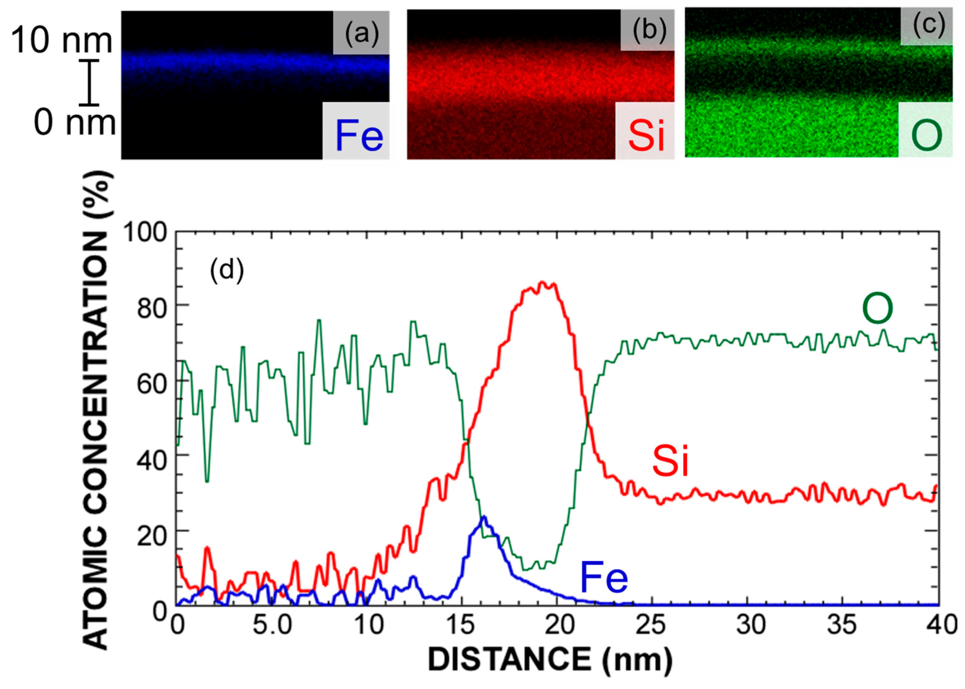
3. Formation of Ultrathin Si/Fe-Silicide/Si Structures
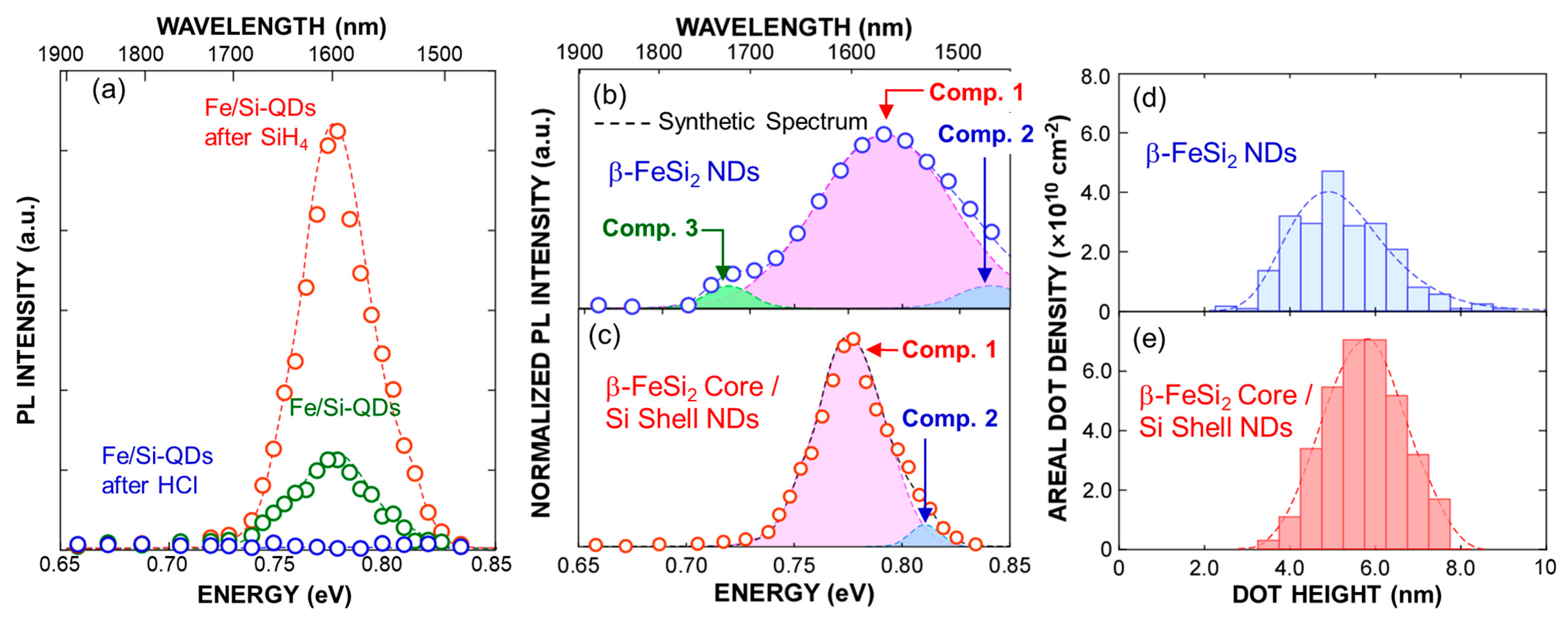
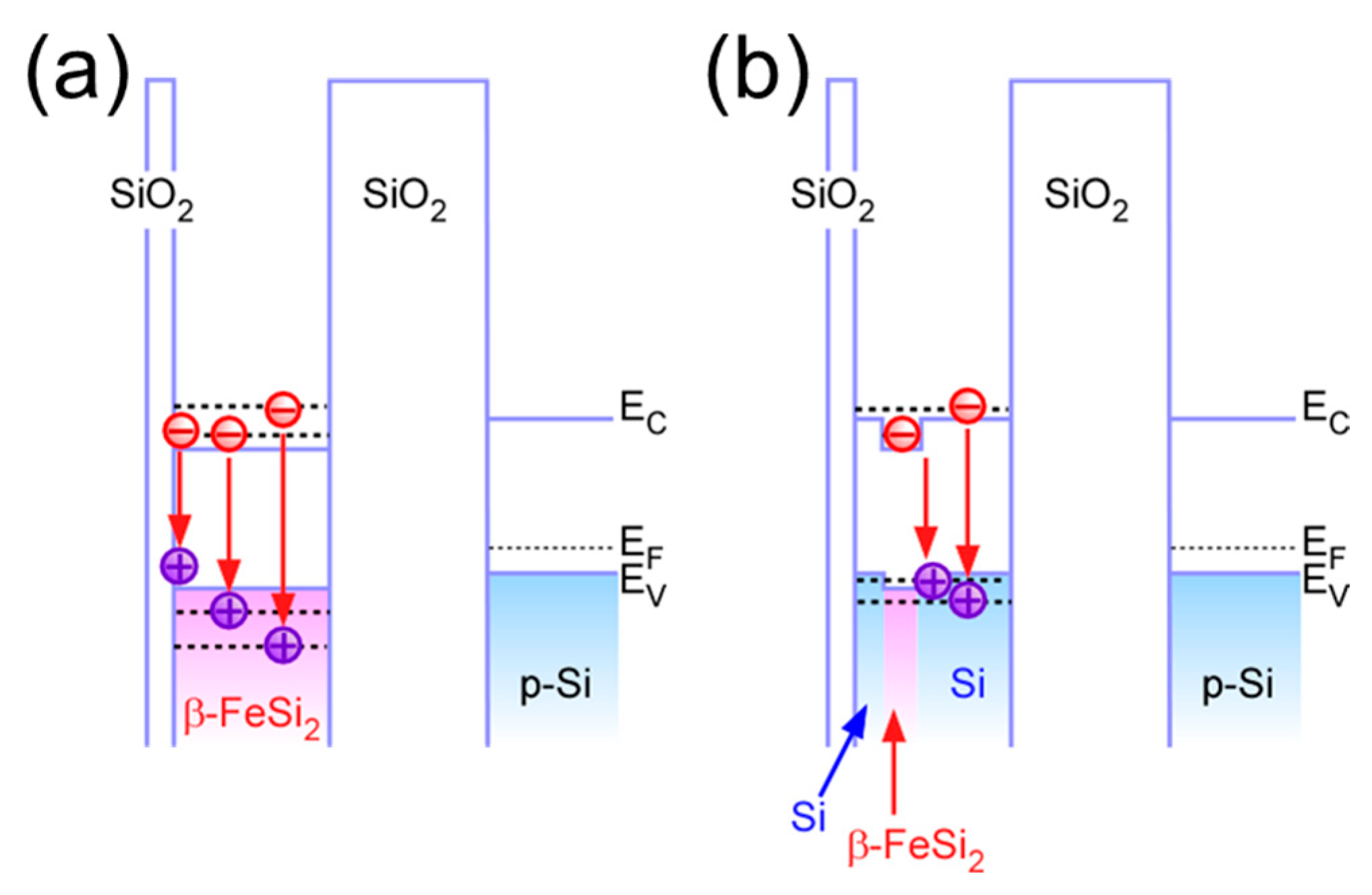
4. Formation and Light Emission Properties of Fe-Silicide Core/Si-Shell Quantum Dots
5. Conclusions
Author Contributions
Funding
Data Availability Statement
Acknowledgments
Conflicts of Interest
References
- Soref, R.A.; Lorenzo, J.P. Single-crystal silicon: A new material for 1.3 and 1.6 μm integrated-optical components. Electron. Lett. 1985, 21, 953–954. [Google Scholar] [CrossRef]
- Schmidtchen, J.; Splett, A.; Schüppert, B.; Petermann, K.; Burbach, G. Low loss singlemode optical waveguides with large cross-section in silicon-on-insulator. Electron. Lett. 1991, 27, 1486–1488. [Google Scholar] [CrossRef]
- Weiss, B.L.; Reed, G.T.; Toh, S.K.; Soref, R.A.; Namavar, F. Optical waveguides in SIMOX structures. IEEE Photonics Technol. Lett. 1991, 3, 19–21. [Google Scholar] [CrossRef] [PubMed]
- Liu, A.; Jones, R.; Liao, L.; Samara-Rubio, D.; Rubin, D.; Cohen, O.; Nicolaescu, R.; Paniccia, M. A high-speed silicon optical modulator based on a metal–oxide–semiconductor capacitor. Nature 2004, 427, 615–618. [Google Scholar] [CrossRef]
- Liao, L.; Samara-Rubio, D.; Morse, M.; Liu, A.; Hodge, D.; Rubin, D.; Keil, U.D.; Franck, T. High speed silicon mach-zehnder modulator. Opt. Express 2005, 13, 3129–3135. [Google Scholar] [CrossRef]
- Liao, L.; Liu, A.; Rubin, D.; Basak, J.; Chetrit, Y.; Nguyen, H.; Cohen, R.; Izhaky, N.; Paniccia, M. 40 Gbit/s silicon optical modulator for high-speed applications. Electron. Lett. 2007, 43, 1196–1197. [Google Scholar] [CrossRef]
- Dehlinger, G.; Koester, S.J.; Schaub, J.D.; Chu, J.O.; Ouyang, Q.C.; Grill, A. High-speed Germanium-on-SOI lateral PIN photodiodes. IEEE Photonics Technol. Lett. 2004, 16, 2547–2549. [Google Scholar] [CrossRef]
- Ahn, D.; Hong, C.-Y.; Liu, J.; Giziewicz, W.; Beals, M.; Kimerling, L.C.; Michel, J.; Chen, J.; Kärtner, F.X. High performance, waveguide integrated Ge photodetectors. Opt. Express 2007, 15, 3916–3921. [Google Scholar] [CrossRef]
- Shekhar, S.; Bogaerts, W.; Chrostowski, L.; Bowers, J.E.; Hochberg, M.; Soref, R.; Shastri, B.J. Roadmapping the next generation of silicon photonics. Nat. Commun. 2024, 10, 751. [Google Scholar] [CrossRef]
- Zakharov, N.D.; Talalaev, V.G.; Werner, P.; Tonkikh, A.A.; Cirlin, G.E. Room-temperature light emission from a highly strained Si/Ge superlattice. Appl. Phys. Lett. 2003, 83, 3084–3086. [Google Scholar] [CrossRef]
- Jambois, O.; Rinnert, H.; Devaux, X.; Vergnat, M. Photoluminescence and electroluminescence of size-controlled silicon nanocrystallites embedded in SiO2 thin films. J. Appl. Phys. 2005, 98, 046105. [Google Scholar] [CrossRef]
- Sun, K.W.; Sue, S.H.; Liu, C.W. Visible photoluminescence from Ge quantum dots. Phys. E Low-Dimens. Syst. Nanostruct. 2005, 28, 525–530. [Google Scholar] [CrossRef]
- del Pino, A.P.; Gyorgy, E.; Marcus, I.C.; Roqueta, J.; Alonso, M.I. Effects of pulsed laser radiation on epitaxial self-assembled Ge quantum dots grown on Si substrates. Nanotechnology 2011, 22, 295304. [Google Scholar] [CrossRef] [PubMed]
- Gassenq, A.; Guilloy, K.; Pauc, N.; Hartmann, J.-M.; Dias, G.O.; Rouchon, D.; Tardif, S.; Escalante, J.; Duchemin, I.; Niquet, Y.-M.; et al. Study of the light emission in Ge layers and strained membranes on Si substrates. Thin Solid Films 2016, 613, 64–67. [Google Scholar] [CrossRef]
- Schlykow, V.; Zaumseil, P.; Schubert, M.A.; Skibitzki, O.; Yamamoto, Y.; Klesse, W.M.; Hou, Y.; Virgilio, M.; De Seta, M.; Di Gaspare, L.; et al. Photoluminescence from GeSn nano-heterostructures. Nanotechnology 2018, 29, 415702. [Google Scholar] [CrossRef]
- Thai, Q.M.; Pauc, N.; Aubin, J.; Bertrand, M.; Chrétien, J.; Delaye, V.; Chelnokov, A.; Hartmann, J.-M.; Reboud, V.; Calvo, V. GeSn heterostructure micro-disk laser operating at 230 K. Opt. Express 2018, 26, 32500–32508. [Google Scholar] [CrossRef]
- Von den Driesch, N.; Stange, D.; Rainko, D.; Breuer, U.; Capellini, G.; Hartmann, J.-M.; Sigg, H.; Mantl, S.; Grützmacher, D.; Buca, D. Epitaxy of Si-Ge-Sn-based heterostructures for CMOS-integratable light emitters. Solid-State Electron. 2019, 155, 139–143. [Google Scholar] [CrossRef]
- Chrétien, J.; Pauc, N.; Pilon, F.A.; Bertrand, M.; Thai, Q.-M.; Casiez, L.; Bernier, N.; Dansas, H.; Gergaud, P.; Delamadeleine, E.; et al. GeSn Lasers Covering a Wide Wavelength Range Thanks to Uniaxial Tensile Strain. ACS Photonics 2019, 6, 2462–2469. [Google Scholar] [CrossRef]
- Armand Pilon, F.T.; Lyasota, A.; Niquet, Y.-M.; Reboud, V.; Calvo, V.; Pauc, N.; Widiez, J.; Bonzon, C.; Hartmann, J.-M.; Chelnokov, A.; et al. Lasing in strained germanium microbridges. Nat. Commun. 2019, 10, 2724. [Google Scholar] [CrossRef]
- Fadaly, E.M.T.; Dijkstra, A.; Suckert, J.R.; Ziss, D.; van Tilburg, M.A.J.; Mao, C.; Ren, Y.; van Lange, V.T.; Korzun, K.; Kölling, S.; et al. Direct bandgap emission from hexagonal Ge and SiGe alloys. Nature 2020, 580, 205–209. [Google Scholar] [CrossRef]
- Ji, Z.-M.; Luo, J.-W.; Li, S.-S. Interface-engineering enhanced light emission from Si/Ge quantum dots. New J. Phys. 2020, 22, 093037. [Google Scholar] [CrossRef]
- Jannesari, R.; Schatzl, M.; Hackl, F.; Glaser, M.; Hingerl, K.; Fromherz, T.; Schäffler, F. Commensurate germanium light emitters in silicon-on-insulator photonic crystal slabs. Opt. Express 2014, 22, 25426–25435. [Google Scholar] [CrossRef] [PubMed]
- Petykiewicz, J.; Nam, D.; Sukhdeo, D.S.; Gupta, S.; Buckley, S.; Piggott, A.Y.; Vučković, J.; Saraswat, K.C. Direct Bandgap Light Emission from Strained Germanium Nanowires Coupled with High-Q Nanophotonic Cavities. Nano Lett. 2016, 16, 2168–2173. [Google Scholar] [CrossRef] [PubMed]
- Reboud, V.; Gassenq, A.; Hartmann, J.M.; Widiez, J.; Virot, L.; Aubin, J.; Guilloy, K.; Tardif, S.; Fédéli, J.M.; Pauc, N.; et al. Germanium based photonic components toward a full silicon/germanium photonic platform. Prog. Cryst. Growth Charact. Mater. 2017, 63, 1–24. [Google Scholar] [CrossRef]
- Walters, R.J.; Bourianoff, G.I.; Atwater, H.A. Field-effect electroluminescence in silicon nanocrystals. Nat. Mater. 2005, 4, 143–146. [Google Scholar] [CrossRef]
- Xu, X.; Tsuboi, T.; Chiba, T.; Usami, N.; Maruizumi, T.; Shiraki, Y. Silicon-based current-injected light emitting diodes with Ge self-assembled quantum dots embedded in photonic crystal nanocavities. Opt. Express 2012, 20, 14714–14721. [Google Scholar] [CrossRef]
- Xu, X.; Usami, N.; Maruizumi, T.; Shiraki, Y. Enhancement of light emission from Ge quantum dots by photonic crystal nanocavities at room-temperature. J. Cryst. Growth 2013, 378, 636. [Google Scholar] [CrossRef]
- Xu, X.; Maruizumi, T.; Shiraki, Y. Waveguide-integrated microdisk light-emitting diode and photodetector based on Ge quantum dots. Opt. Express 2014, 22, 3902–3910. [Google Scholar] [CrossRef]
- Zeng, C.; Ma, Y.; Zhang, Y.; Li, D.; Huang, Z.; Wang, Y.; Huang, Q.; Li, J.; Zhong, Z.; Yu, J.; et al. Single germanium quantum dot embedded in photonic crystal nanocavity for light emitter on silicon chip. Opt. Express 2015, 23, 22250–22261. [Google Scholar] [CrossRef]
- Makihara, K.; Kondo, K.; Ikeda, M.; Ohta, A.; Miyazaki, S. Photoluminescence Study of Si Quantum Dots with Ge Core. ECS Trans. 2014, 64, 365–370. [Google Scholar] [CrossRef]
- Yamada, K.; Kondo, K.; Makihara, K.; Ikeda, M.; Ohta, A.; Miyazaki, S. Effect of Ge Core Size on Photoluminescence from Si Quantum Dots with Ge Core. ECS Trans. 2016, 75, 695–700. [Google Scholar] [CrossRef]
- Kondo, K.; Makihara, K.; Ikeda, M.; Miyazaki, S. Photoluminescence study of high density Si quantum dots with Ge core. J. Appl. Phys. 2016, 119, 033103. [Google Scholar] [CrossRef]
- Makihara, K.; Ikeda, M.; Fujimura, N.; Yamada, K.; Ohta, A.; Miyazaki, S. Electroluminescence of superatom-like Ge-core/Si-shell quantum dots by alternate field-effect-induced carrier injection. Appl. Phys. Express 2018, 11, 011305. [Google Scholar] [CrossRef]
- Makihara, K.; Yamamoto, Y.; Imai, Y.; Taoka, N.; Schubert, M.A.; Tillack, B.; Miyazaki, S. Room Temperature Light Emission from Superatom–like Ge–core/Si–shell Quantum Dots. Nanomaterials 2023, 13, 1475. [Google Scholar] [CrossRef]
- Bost, M.C.; Mahan, J.E. Optical properties of semiconducting iron disilicide thin films. J. Appl. Phys. 1985, 58, 2696–2703. [Google Scholar] [CrossRef]
- Katsumata, H.; Makita, Y.; Kobayashi, N.; Shibata, H.; Hasegawa, M.; Aksenov, I.; Kimura, S.; Obara, A.; Uekusa, S.-I. Optical absorption and photoluminescence studies of β-FeSi2 prepared by heavy implantation of Fe+ ions into Si. J. Appl. Phys. 1996, 80, 5955–5962. [Google Scholar] [CrossRef]
- Leong, D.; Harry, M.; Reeson, K.J.; Homewood, K.P. A silicon/iron-disilicide light-emitting diode operating at a wavelength of 1.5 μm. Nature 1997, 387, 686–688. [Google Scholar] [CrossRef]
- Suemasu, T.; Negishi, Y.; Takakura, K.; Hasegawa, F.; Chikyow, T. Influence of Si growth temperature for embedding β-FeSi2 and resultant strain in β-FeSi2 on light emission from p-Si/β-FeSi2 particles/n-Si light-emitting diodes. Appl. Phys. Lett. 2001, 79, 1804–1806. [Google Scholar] [CrossRef]
- Nakamura, T.; Tatsumi, T.; Morita, K.; Kobayashi, H.; Noguchi, Y.; Kawakubo, Y.; Maeda, Y. Photoluminescence Property of Nano-Composite Phases of β-FeSi2 Nanocrystals Embedded in SiO2. JJAP Conf. Proc. 2015, 3, 011106. [Google Scholar] [CrossRef]
- Lourenco, M.A.; Butler, T.M.; Kewell, A.K.; Gwilliam, R.M.; Kirkby, K.J.; Homewood, K.P. Electroluminescence of β-FeSi2 Light Emitting Devices. Jpn. J. Appl. Phys. 2001, 40, 4041–4044. [Google Scholar] [CrossRef]
- Martinelli, L.; Grilli, E.; Guzzi, M.; Grimaldi, M.G. Room-temperature electroluminescence of ion-beam-synthesized β-FeSi2 precipitates in silicon. Appl. Phys. Lett. 2003, 83, 794. [Google Scholar] [CrossRef]
- Li, C.; Ozawa, Y.; Suemasu, T.; Hasegawa, F. Thermal Enhancement of 1.6 µm Electroluminescence from a Si-Based Light-Emitting Diode with β-FeSi2 Active Region. Jpn. J. Appl. Phys. 2004, 43, L1492. [Google Scholar]
- Sunohara, T.; Kobayashi, K.; Suemasu, T. Epitaxial growth and characterization of Si-based light-emitting Si/β-FeSi2 film/Si double heterostructures on Si(001) substrates by molecular beam epitaxy. Thin Solid Films 2006, 508, 371–375. [Google Scholar] [CrossRef]
- Miyazaki, S.; Hamamoto, Y.; Yoshida, E.; Ikeda, M.; Hirose, M. Control of Self-Assembling Formation of Nanometer Silicon Dots by Low Pressure Chemical Vapor Deposition. Thin Solid Films 2000, 369, 55–59. [Google Scholar] [CrossRef]
- Takami, H.; Makihara, K.; Ikeda, M.; Miyazaki, S. Characterization of Electroluminescence from One-dimensionally Self-Aligned Si-based Quantum Dots. Jpn. J. Appl. Phys. 2013, 52, 04CG08. [Google Scholar] [CrossRef]
- Yamada, T.; Makihara, K.; Ohta, A.; Ikeda, M.; Miyazaki, S. Study on electroluminescence from multiply-stacking valency controlled Si quantum dots. Thin Solid Films 2016, 602, 48–51. [Google Scholar] [CrossRef]
- Furuhata, H.; Makihara, K.; Shimura, Y.; Fujimori, S.; Imai, Y.; Ohta, A.; Taoka, N.; Miyazaki, S. Study on Silicidation Reaction of Fe-NDs with SiH4. Appl. Phys. Express 2022, 15, 055503. [Google Scholar] [CrossRef]
- Miyazaki, S.; Makihara, K. Formation and Characterization of Fe-Silicide Nanodots for Optoelectronic Application. ECS Trans. 2023, 112, 131–137. [Google Scholar] [CrossRef]
- Saito, H.; Makihara, K.; Taoka, N.; Miyazaki, S. Formation of β-FeSi2 NDs by SiH4-exposure to Fe-NDs. Jpn. J. Appl. Phys. 2024, 63, 02SP99. [Google Scholar] [CrossRef]
- Canali, C.; Majni, G.; Ottaviani, G.; Celotti, G. Phase diagrams and metal-rich silicide formation. J. Appl. Phys. 1979, 50, 255–258. [Google Scholar] [CrossRef]
- Ikarashi, N.; Masuzaki, K. Silicide formation process in ultra-thin Ni-silicide film for advanced semiconductor devices: Mechanism of NiSi2 formation at low temperature. J. Phys. Conf. Ser. 2011, 326, 012051. [Google Scholar] [CrossRef]


Disclaimer/Publisher’s Note: The statements, opinions and data contained in all publications are solely those of the individual author(s) and contributor(s) and not of MDPI and/or the editor(s). MDPI and/or the editor(s) disclaim responsibility for any injury to people or property resulting from any ideas, methods, instructions or products referred to in the content. |
© 2025 by the authors. Licensee MDPI, Basel, Switzerland. This article is an open access article distributed under the terms and conditions of the Creative Commons Attribution (CC BY) license (https://creativecommons.org/licenses/by/4.0/).
Share and Cite
Makihara, K.; Yamamoto, Y.; Schubert, M.A.; Mai, A.; Miyazaki, S. Processing and Characterization of High-Density Fe-Silicide/Si Core–Shell Quantum Dots for Light Emission. Nanomaterials 2025, 15, 733. https://doi.org/10.3390/nano15100733
Makihara K, Yamamoto Y, Schubert MA, Mai A, Miyazaki S. Processing and Characterization of High-Density Fe-Silicide/Si Core–Shell Quantum Dots for Light Emission. Nanomaterials. 2025; 15(10):733. https://doi.org/10.3390/nano15100733
Chicago/Turabian StyleMakihara, Katsunori, Yuji Yamamoto, Markus Andreas Schubert, Andreas Mai, and Seiichi Miyazaki. 2025. "Processing and Characterization of High-Density Fe-Silicide/Si Core–Shell Quantum Dots for Light Emission" Nanomaterials 15, no. 10: 733. https://doi.org/10.3390/nano15100733
APA StyleMakihara, K., Yamamoto, Y., Schubert, M. A., Mai, A., & Miyazaki, S. (2025). Processing and Characterization of High-Density Fe-Silicide/Si Core–Shell Quantum Dots for Light Emission. Nanomaterials, 15(10), 733. https://doi.org/10.3390/nano15100733