1. Introduction
Amorphous oxides (TaO
x, ZrO
x) [
1,
2,
3,
4,
5] and bulk phase change materials (VO
2/V
2O
5) [
6] are showing tremendous potential as active layer materials for resistive random access memory (ReRAM) materials. These oxides are compatible with existing complementary metal oxide semiconductor (CMOS) fabrication methods and have unique functional properties, such as the ability for in-memory analog computations, that could allow them to complement or replace conventional CMOS-based devices. For example, Ta
2O
5 has shown sub-nanosecond switching [
7], low switching voltage (~1 V), long state retention (>10 years), and high switching endurance (>10
10 cycles) [
2]. Arrays of Pd/TaO
x/Ta/Pd cross bar devices have demonstrated complex computational tasks with improved energy efficiency and throughput compared to digital systems [
8]. The resistive switching mechanisms in these materials are driven by oxygen migration and typically require an initial electroforming step, wherein the film is switched from a high-resistance to a low-resistance state. This electroforming step is not fully understood and has not been thoroughly replicated in computational models [
9], and is not always required for stable resistive switching [
10]. However, it is generally considered important for initiating the onset of oxygen motion in highly insulating oxide films. This oxygen motion can be driven both in and out of the plane of the TaO
x layer, where the mechanism and the resulting resistive switching IV characteristics were shown by Lee et al. [
2]. This mechanism shows a local movement of oxygen from the Ta
2O
5-x layer into a TaO
2-x layer, forming metallic filaments through the Ta
2O
5-x layer and a buildup of oxygen at the Ta
2O
5-x/TaO
2-x interface [
2]. This process can be seen in the IV characteristics of the material and is typically seen as a sharp increase in current at the set voltage (V
set) where the metallic filaments are formed. Lee et al. subsequently demonstrated the effect that the active layers [
2] and electrode materials have on the device characteristics [
3]. In situ transmission electron microscopy (TEM) was used to image the oxygen motion in the active layers and showed that, by decreasing the interface roughness between the top electrode and the Ta
2O
5-x layer, the device behavior transitions from being dominated by filament formation to behavior that is dictated by the buildup of interfacial oxygen [
3]. This suggests that rough interfaces can enable localization of the electric field and drive filament formation. The effects of silicon doping of TaO
x was studied by Kim et al., [
11] where the doped devices showed higher on/off ratios, suggesting a larger depletion gap between the filament and electrode. This larger depletion gap was attributed to a higher oxygen mobility in the Si-doped tantalum oxide compared to the undoped oxide. This increase in oxygen motion was rationalized by the induction of oxygen mobility channels generated by stronger bonding in the Si-O bond relative to Ta-O.
Ta:ZrO systems, deposited by atomic layer deposition (ALD), have also been investigated by Kukli et al. [
12], finding that the chemistry with a low zirconium concentration (Zr:Ta atomic ratio of 0.2) exhibited the largest hysteresis and most consistent switching. This chemistry showed the highest crystallization temperature (800 °C) forming a δ-Ta
2O
5 phase. Crystallization eliminated all hysteretic behavior for each chemistry studied, suggesting that the mechanism for resistive switching in these Zr
xTa
1−xO
y chemistries requires vacancy-driven ion movement, which requires less energy in amorphous systems. Kukli et al. [
12] showed that hysteresis is dependent on the Zr:Ta ratio and that this hysteresis requires an amorphous structure, suggesting that modulating the Zr:Ta ratio has an effect on the vacancy concentration of the oxide layer.
Combinatorial synthesis of Y:Zr
xTa
1−xO
y by pulsed laser deposition (PLD) was conducted by Kiyota et al. [
13]. The system consisted of a consistent 10 atomic % YO
x and a compositional gradient of Ta and Zr. A minimum in the dielectric constant (k) of 18 was found at 30% ZrO
2 and then steadily increased to 22 with increasing Ta
2O
5. However, the leakage current also steadily increased with increasing Ta
2O
5. Zrinski et al. [
14] investigated a combinatorial system of Ta
xHf
1−xO
y deposited by magnetron sputtering and a subsequent wet electrochemical anodization process to oxidize the topmost 20 nm of the film. Current-voltage measurements revealed that the high-Hf concentration zone exhibited poor resistive switching behavior, while the low-Hf zone did not show any improvements compared to Ta
2O
5. Ratios between 50 and 70 atomic % Hf showed on/off ratios of eight orders of magnitude with device endurance reaching one million cycles. This region exhibited unipolar switching compared to the high and low Hf regions, which exhibited bipolar switching. This unipolar switching was driven by HfO
2 crystallites present in the otherwise amorphous oxide.
Doolittle et al. observed resistive switching that was attributed to charge trapping in defect states in Nb
2O
5-x films [
15]. These Nb
2O
5-x devices generated current-voltage hysteresis at low frequencies by increasing voltage over the onset voltage needed to transition from Schottky emission to tunneling transport through the highly charged interface layer of the film. This topmost layer causes the turn on voltage to be dictated by the Schottky barrier height. Beyond the turn-on voltage, the devices transition to a Fowler–Nordheim (FN) tunneling/Poole–Frenkel (PF) mechanism that dictates the hysteretic behavior. Kim et al. also produced charge trapping-based Nb
2O
5-x memristors, but in order to stabilize the high and low-resistance states, Ta
2O
5 and Al
2O
3-y capping layers were inserted between the Nb
2O
5-x active layer and Pt and Ti electrodes, respectively [
16]. The Ta
2O
5 layer prevented the discharge of energized trap states in the active layer to the Pt electrode, stabilizing the low-resistance state (LRS). The Al
2O
3-y layer prevented charge migration from the Ti electrode to empty trap states in the active layer, thus stabilizing the high-resistance state (HRS). Similarly, electroforming-free hysteretic current-voltage behavior was shown by Yoon et al. [
17] using a Pt/Ta
2O
5/HfO
2-x/TiN device stack that employed ALD to deposit the Ta
2O
5 and HfO
2-x active layers.
Reservoir computing (RC) has emerged as a powerful and energy-efficient paradigm for processing time-dependent information by utilizing the dynamics of nonlinear electrical systems. Unlike traditional recurrent neural networks, RC fixes the internal reservoir weights and trains only the output layer, greatly simplifying the training process while maintaining high computational capability for tasks such as pattern recognition, classification, and temporal prediction. Recent advances have demonstrated that volatile memristive devices are excellent candidates for physical reservoir computing because of their intrinsic short-term memory behavior and nonlinear, history-dependent conductance modulation. Ju et al. implemented an 8-bit reservoir computing system using volatile ITO/ZrO
x/TaN memristors, exploiting gradual interface-type resistive switching and current decay phenomena to achieve high-dimensional temporal mapping and efficient multi-level data storage [
18]. A similar approach has also been reported using Pt/BFO/SRO/STO ferroelectric devices [
19], highlighting the critical role of volatile resistive switching in constructing scalable, energy-efficient, and neuromorphic-compatible reservoir architectures.
This work leverages combinatorial thin-film sputtering to rapidly explore the ReRAM properties of mixed valence transition metal oxide active layers, where co-sputtering Ta and Zr metal targets in an Ar-O2 ambient generates a compositional gradient of mixed oxidation states. Chemical composition and valence state were correlated to local current-voltage measurements via X-ray photoelectron spectroscopy (XPS) and time-of-flight secondary ion mass spectrometry (ToF-SIMS) to elucidate the resistive switching mechanisms operative in the ZrxTa1−xOy system.
2. Materials and Methods
Plane-wave density functional theory (DFT) calculations were carried out using Vienna Ab initio Simulation Package (VASP), version 6.5, and the projector-augmented wave (PAW) pseudopotentials for electron–ion interactions [
20]. Exchange–correlation interactions were accounted for using the generalized gradient approximation (GGA) functional of Perdew–Burke–Ernzerhof (PBE) [
21]. A previous model was used for amorphous tantalum oxide. That model was based on a super cell of crystalline Ta
2O
5, containing 168 atoms (Ta
48O
120 [
22,
23]) with optimized lattice constants of
x = 14.635 Å,
y = 12.377 Å, and
z = 11.761 Å. During structural optimization, the atoms and cell volume relaxed until the residual forces fell below 0.02 eV/Å, with a cutoff energy of 520 eV and Gamma-point k-point sampling. To generate an amorphous structure, ab-initio molecular dynamics (AIMD) simulations were used in a melt-and-quench approach. This model and its oxygen vacancy derivatives has shown very good agreement with experimental cathode luminescence (CL), electron energy loss spectroscopy (EELS), and scanning microwave impedance microscopy (SMIM) [
24]. In this study, starting with amorphous Ta
48O
119, AIMD was run using a Nose–Hoover thermostat at room temperature and used the mean square displacement (MSD) of O via Einstein’s relation to find the respective diffusion coefficients. Following this simulation protocol, Zr was doped into the model following Zr
xTa
1−xO
y; with x = 5, 15, 20 which corresponds to 10%, 31%, and 42% Zr doping. The largest MSD for oxygen and subsequently the highest diffusion coefficient was found to occur at a doping level of 31% Zr (see
Supplemental Figure S1).
A 5 nm Ti adhesion layer was deposited using DC magnetron sputtering onto a thermally grown SiO
2 (500 nm)-coated silicon substrate. The bottom 40 nm Pt electrode was subsequently deposited on the Ti adhesion layer via magnetron sputtering. Ta(20 nm)/Zr
xTa
1−xO
y(10–15 nm) active layers were deposited on top of the Pt(40 nm) bottom electrode. The metallic Ta layer was deposited with an applied power of 100 W DC for 1 min 50 s with substrate rotation on to realize a uniform film thickness. The combinatorial Zr
xTa
1−xO
y layer was deposited with an applied power of 38 W DC on the Ta target and 100 W DC on the Zr target with a 25/5.2 sccm Ar/O
2 flow rate ratio and 5 mTorr pressure for 5 min and 50 s with the substrate stationary to realize the combinatorial gradient. X-ray reflectometry (XRR) was used to measure the center thickness of the deposited layers (see
Supplemental Figure S2) and energy dispersive spectroscopy (EDS) was used to verify the composition gradient of the film across the 100 mm substrate. Grazing incidence X-ray diffraction (GIXRD) was used to confirm the amorphous structure of the film (see
Supplemental Figure S3). A PANalytical X’Pert Pro MRD equipped with a proportional Xenon counter was used for the XRR measurement and GIXRD, while a Zeiss Merlin SEM was used for the EDS measurement. XPS was also used to measure the composition and elucidate the bonding/valence characteristics in the films as the cation ratio varies across the sample. Films with pure Ta
2O
5 and ZrO
2 were also fabricated using the same parameters but with substrate rotation on to reduce thickness gradients.
Then, 100 mm diameter, 40 nm thick top Pt electrode pads were DC magnetron sputter-deposited via a photolithographically patterned lift-off process. Electrical cycling measurements were performed by biasing the Pt top electrodes with a Keithley 2400 source measure unit (SMU) while the continuous bottom Pt electrode was grounded. The electrical measurements were conducted along the Zr
xTa
1−xO
y composition gradient at various electrode positions representative of various stoichiometries. Each DC electrical cycle had a constant 1 min cycle time and consisted of 400 voltage increments where the voltage increment varied based on the voltage range studied. The leakage current behavior over time was measured using a Keithley 4200A-SCS parameter analyzer, manufactured by Tektronix (Beaverton, OR, USA). All electrical measurements utilized a Form Factor Cascade CM300xi probe station. A diagram of the film stack along with the corresponding band diagram is illustrated in
Figure 1. Also shown in
Figure 1 is the estimated cation composition gradient and thickness across the 100 mm diameter substrate.
Time-of-flight secondary ion mass spectrometry (ToF-SIMS) system, ToF.SIMS 5 by
iONTOF (Münster, Germany), was used to profile pristine and cycled devices. An alternating sputter of Cs
+ and Bi
3+ was used to profile and image the device. A 1 keV Cs
+ ion beam was rastered in a 500 × 500 µm
2 area to form a sputtered crater for 20 frames. Four frames of a 30 keV Bi
3+ ion beam were used to raster a 100 × 100 µm
2 area. An electron flood gun was used to mitigate charging during profiling.
Figure S4a,c,e,f show images of the CsPt
+ ion count in order to show the relative position of the device centered in the ion beam raster.
Figure S4b,d,f,h show the areas of interest that were used for the depth profiles to isolate ions from the device and exclude ions from the native film in the corners of the 100 × 100 µm
2 scan.
3. Results and Discussion
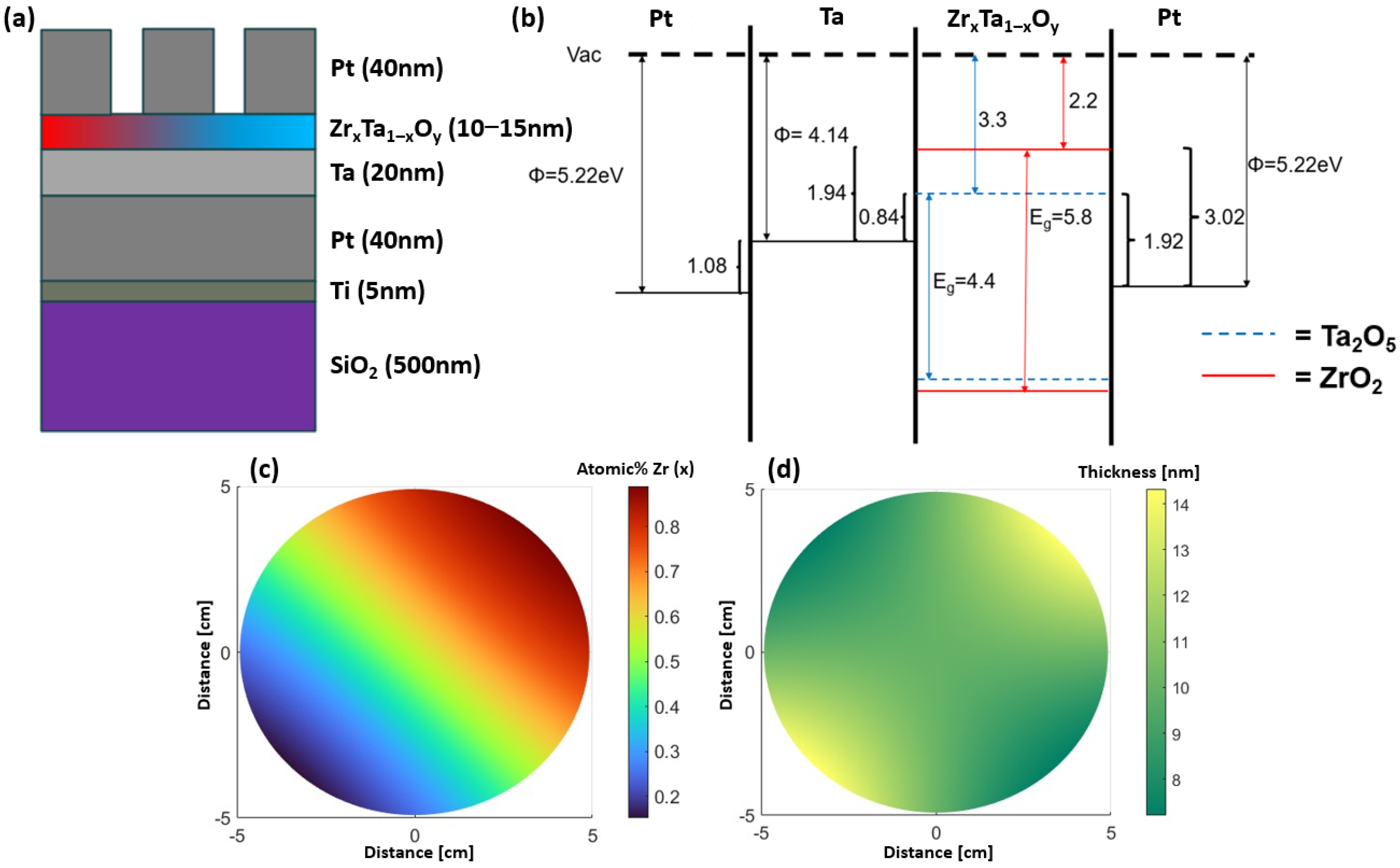
The device film stack geometry can be found below in
Figure 1a, alongside the theoretical band diagram (
Figure 1b). The band diagram of the film stack illustrates the large barrier to charge injection from the top Pt electrode as compared to injection from the bottom Pt/Ta electrode. The predicted cation concentration (
Figure 1c) and thickness (
Figure 1d) of the memristive oxide layers were simulated across the wafer; many of the parameters that are relevant for the sputtering system were experimentally determined in the previous work [
25].
Figure 1.
Schematic of the (
a) thin film stack and (
b) the expected band diagram of the devices. Schematic of (
c) simulated cation atomic % Zr (note that atomic % Ta is 1−atomic % Zr), and (
d) thickness of the combinatorial Zr
xTa
1−xO
y layer. The ZrO
2 bandgap was taken from Li et al. [
26], Ta
2O
5 bandgap from Zhuo et al. [
27], while Pt and Ta work functions were taken from Mechtly [
28].
Figure S2 shows a XRR thickness measurement at the center of the combinatorial wafer while
Figure S5 compares the measured (EDS) and simulated [
25] Ta and Zr cation atomic percentage measured along the centerline of the substrate, which are in good agreement. For the results presented below, the cation compositions were estimated from the simulated sputtering model. Calculated mean square displacement (MSD) values were determined at various Ta/Zr ratios and showed an increase in oxygen mobility around 30% Zr. The MSD plot of oxygen for three different Zr doping concentrations is shown in
Figure S1.
Figure 2a–d are XPS spectra for the Ta 4f (and Zr 4p), Ta 3d, O 1s, and the valence band energy regions, respectively. As can be observed, all of the spectra shift to lower binding energy with increasing Zr content. The shifts in the Ta, Zr, and O core levels (b–d) are consistent with observations of Tewg et al. that were attributed to charge transfer mechanisms affecting all three elements in the film [
29]. Namely, as Zr concentration is increased, the positive charge of the cation Ta and Zr decreases and the negative anion charge on the oxygen increases. As noted in the Ta 4f spectra, the Ta
4+ peak increases with increasing Zr, which affirms the decrease in the overall charge on the Ta cations. Interestingly, the valence band also shifts to lower binding energy with increasing Zr content, which is not consistent with the band diagram pictured in
Figure 1. This suggests that perhaps the electron affinity of the Ta
2O
5 is slightly larger or the ZrO
2 is slightly smaller than the diagram suggests; in either case, the conduction band barrier height difference between the ZrO
2 and Ta
2O
5 would be larger than the 1.1 eV represented in
Figure 1.
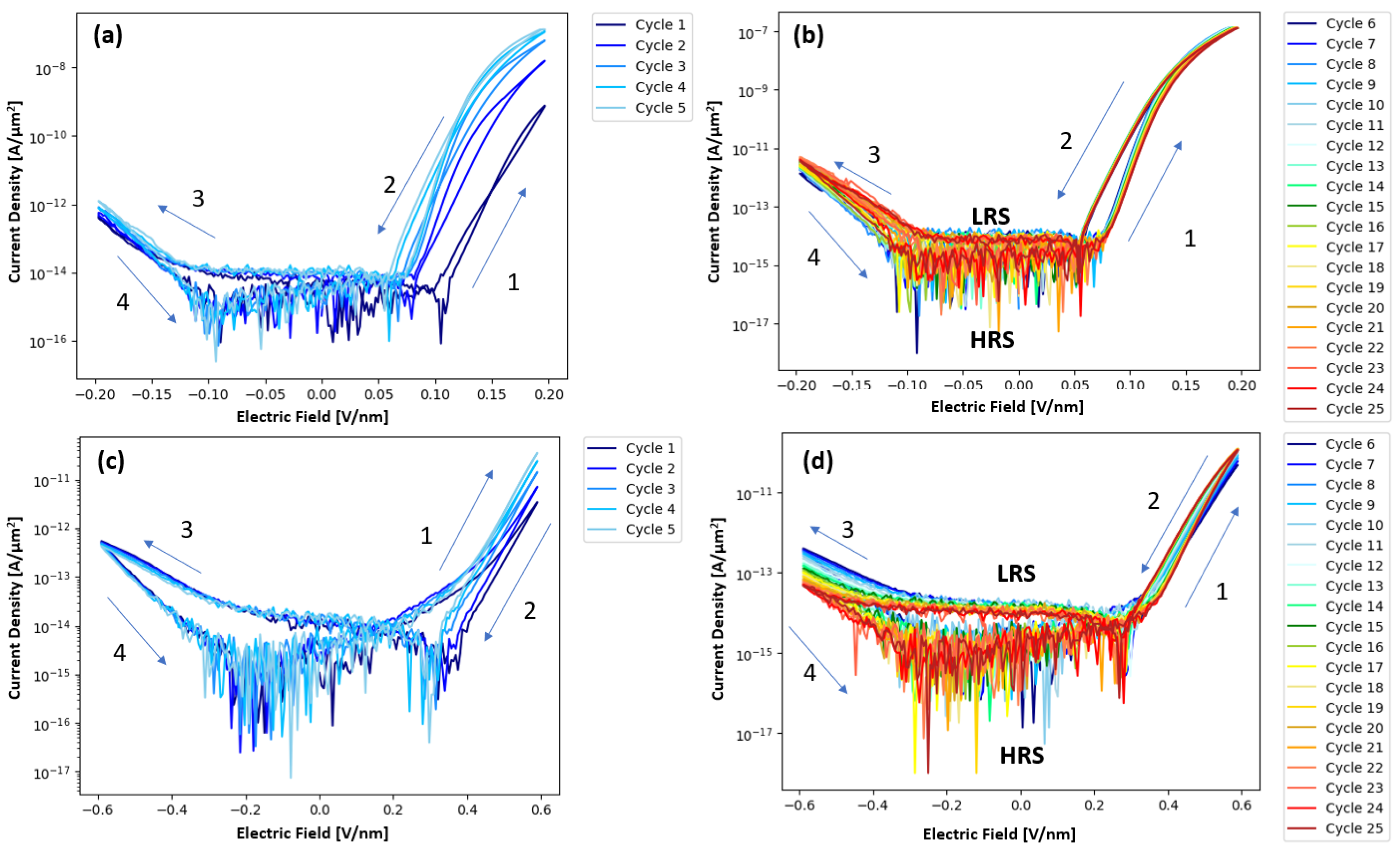
Figure 3a,b illustrate the current density electric field measurements of the pure Ta
2O
5 devices, which revealed a “wake-up” behavior of about five cycles at +/− 0.2 V/nm. After these wakeup cycles, cycles 6–25 showed consistent resistive switching where the devices switch from the HRS to the LRS upon the forward and reverse positive voltage cycle. The post wake-up behavior of both devices shows a distinct turn-on voltage. Arrangement of the probes indicates that the positive voltage cycle is due to electron injection from the Ta interlayer bottom electrode of the device, which is consistent with the lower work function and barrier height for the Ta/Ta
2O
5 interface. The negative voltage sweep for injection from the Pt/Ta
2O
5 top electrode has a much higher barrier height and consequently higher turn-on field and, thus, rectifying behavior. In contrast to the Ta
2O
5 devices,
Figure 3c,d show that the pure ZrO
2 devices exhibit a longer wake up period of about 15 cycles, after which the ZrO
2 devices also exhibit resistive switching from HRS to LRS. Plots showing cycles 6–10, 11–15, 16–20, and 21–25 for a pristine ZrO
2 device can be seen in
Figure S6. During the initial cycling, the ZrO
2 devices exhibit switching from an LRS to an HRS, before slowly transitioning to high-to-low resistance state switching. This transition from LRS/HRS switching to HRS/LRS switching is attributed to a shift from charge capture-controlled PF conduction, where charge capture rate is above the charge emission rate, to emission-controlled PF conduction. This shift is caused by a decrease in trap depth with increased cycling, effectively increasing the charge emission rate. The ZrO
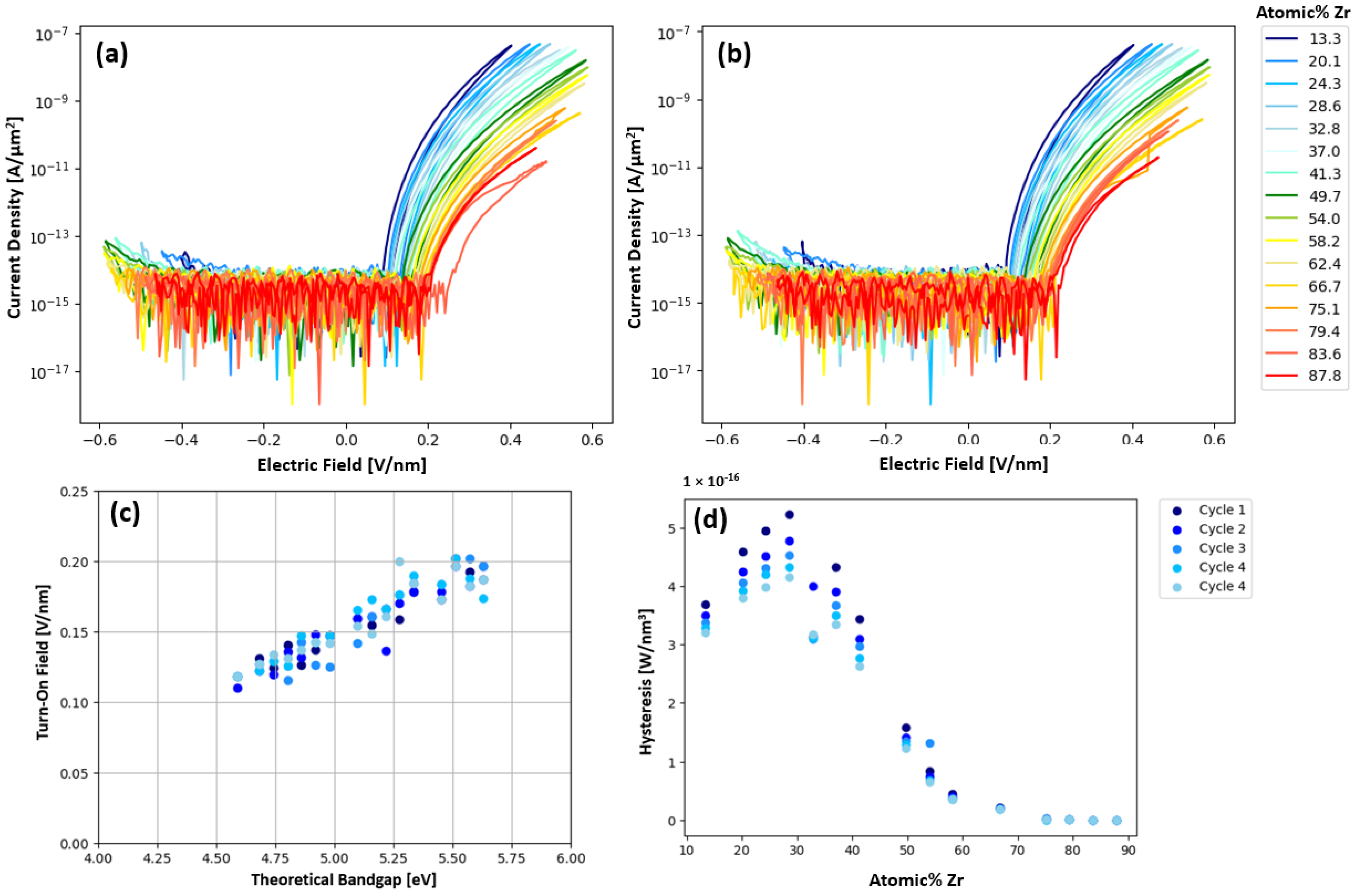
2 devices also show decreasing current (higher resistance) during subsequent negative sweeps and this negative polarity switching did not saturate up to 25 sweeps. When measuring Zr
xTa
1−xO
y combinatorial devices, the wakeup period is not as pronounced compared to the pure Ta
2O
5 or ZrO
2 devices. The current density versus electric field for Zr
xTa
1−xO
y is plotted as a function of the composition (normalized by the thickness gradient from
Figure 1d in
Figure 4a,b for cycle 1 and 5, respectively, where a composition range of 0.133 < x < 0.878 was measured. The turn-on field was defined as the field where the current begins to increase above the low voltage noise.
Figure 4c shows the expected trend, that the turn-on field increases linearly with the theoretical bandgap. The theoretical bandgap was calculated assuming the bandgap scales linearly with Zr content.
Figure 4d shows that hysteresis increases up to about 30% Zr then steadily decreases with increasing Zr. This maximum hysteresis at 30% Zr matches the concentration (30% Zr) found by Kiyota et al. to have the minimum dielectric constant in a Y:Zr
xTa
1−xO
y system [
13]. This maximum hysteresis concentration is also closest to the concentration (Zr:Ta atomic ratio of 0.2) found by Kukli et al. [
12] to have the largest hysteresis and most consistent switching behavior. The AIMD simulations presented in
Figure S1 also show the highest MSD for oxygen at a Zr concentration of 30 atomic percent. This result suggests that ionic motion could also be contributing to the increased hysteresis around 30% Zr region.
To understand the mechanisms responsible for the hysteresis observed in the Zr
xTa
1−xO
y system, various current injection mechanisms that can be operative in metal–insulator–metal (MIM) devices were explored. The current density electric field behavior is similar to what was observed by Doolittle et al. for memristive Nb
2O
5 devices, where Schottky emission was determined to be the primary conduction mechanism prior to the turn-on voltage [
15]. This is supported by
Figure 4c, showing the linear increase in the turn-on field with increasing zirconium content. After current onset, trap-assisted Fowler–Nordheim (FN) tunneling dominates current injection through the highly charged layer at the electrode/Zr
xTa
1−xO
y interface, while Poole–Frankel (PF) charge trapping and emission is responsible for conduction through the remainder of the amorphous Zr
xTa
1−xO
y film. During the reverse sweeps, hysteresis occurs because the emission rate is higher than the charge capture rate, which allows for higher conductivity in the reverse sweep relative to the forward sweep. It is also suspected that a portion of the trap states remain filled during the reverse sweep, effectively increasing the charge emission/capture ratio. This current limited electron capture process is dependent on the emission rate by trap states (
ee),
and charge capture rates (
ce),
where
vth is the carrier thermal velocity,
σn is the electron capture cross section,
n is the density of available electrons,
Nt is density of traps,
Nc is the effective density of states and
Ec−
Et is the trap depth. In this case, the primary charge carrier for this mechanism is electron motion.
This temperature-driven inequality of emission and capture of charge is confirmed in
Figure 5a, where measurements were conducted across a range of temperatures and show that the calculated hysteresis (
Figure S7a) increases with increasing temperature for the five cycles measured. An increase in the maximum current density with temperature is demonstrated in
Figure 5a, which could be explained by an increase in thermal carrier velocity and the number of trap states. This increase in current and hysteresis with temperature also suggests a possible ionic motion contribution to the conduction mechanism. A similar combination of Schottky emission at low voltages and tunneling/PF conduction at higher voltages was observed by Doolittle et al. [
15]. PF conduction is observed at voltages above the turn on voltage while Schottky emission is driven by a highly charged layer at the electrode/active layer interface. Poole–Frankel conduction is described by
where
q is elemental charge,
µ is electron mobility,
N0 is defect concentration,
E is electric field,
ΦD is defect trap energy,
ε is the high-frequency dielectric constant. As shown in
Figure S7b, the defect trap energy (
ΦD) of a device with Zr
3Ta
7O
y was determined to be 1.16 eV from the intercept of a plot of the activation energy versus the square root of electric field (
Figure 5b). This trap energy is significantly higher compared to the trap energy found by Doolittle et al. in Nb
2O
5 (0.22 eV) [
15]. These values for Nb
2O
5 and Zr
xTa
1−xO
y are qualitatively consistent considering Zr
xTa
1−xO
y exhibited a higher onset field (0.125 V/nm versus 0.005–0.09 V/nm in Nb
2O
5). The negative bias portion of the IV cycling shows significantly lower current due to a higher Schottky barrier height at the Pt/oxide interface.
Similar plots for the Ta
2O
5 devices are shown in
Figure S8. The Ta
2O
5 injection shows a decrease in PF trap activation energy with increasing field with a zero-field trap depth of 0.93 eV. The increased trap depth of the Zr
3Ta
7O
y film compared to the pure Ta
2O
5 and ZrO
2 films is attributed to the increasing bandgap with the addition of ZrO
2 to Ta
2O
5 and thus deeper trap states. The increased trap depth also suggests that the conduction mechanism of the mixed Ta/Zr cation film exhibits a similar conduction mechanism to the Ta
2O
5 devices, at least at modest amounts of Zr.
Figure S9 shows the current voltage behavior for the ZrO
2 injection along with the PF activation energy and trap depth calculations. Counter to the Ta
2O
5 injection, the ZrO
2 devices show an increasing PF trap activation energy with increasing field, generating a zero-field trap depth of 0.05 eV. The low trap depth of the ZrO
2 devices suggests that the PF trap-emission mechanism is not the dominate current transport mechanism in the pure ZrO
2 film.
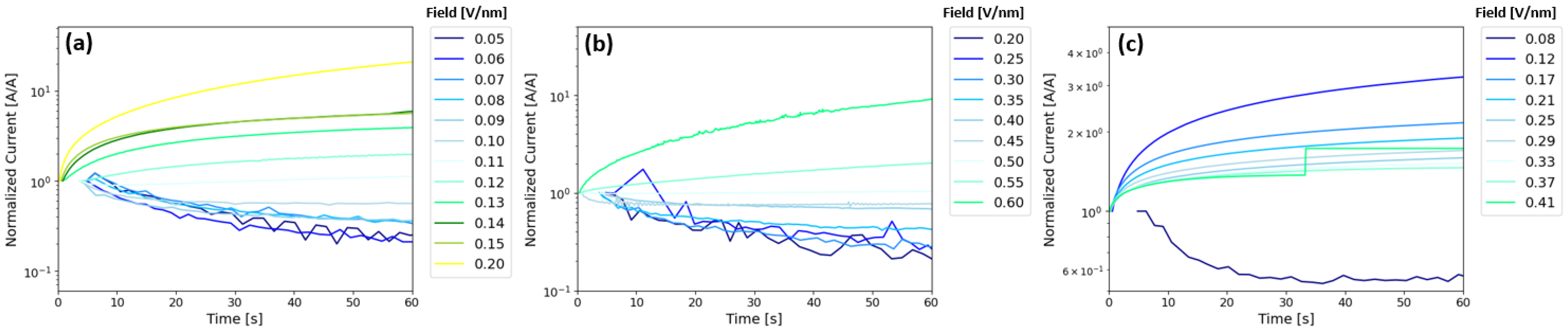
Following Doolittle et al.,
Figure 6 shows normalized current versus time as a function of bias voltage for Ta
2O
5 (
Figure 6a), ZrO
2 (
Figure 6b), and Zr
3Ta
7O
y (
Figure 6c), all poled such that electron injection is from the bottom Pt/Ta electrode (or positive voltage applied to the top Pt contact). See
Figures S10 and S11 for the corresponding absolute values of the current-time plots and initial current density values versus field for each active layer, respectively. The Ta
2O
5 injection shows a decrease in current versus time below the turn-on field (~0.11 V/nm) and a current increase above the turn-on field. This signature is consistent with a transition in the mechanism from Schottky emission below the turn-on field to trap-assisted tunneling and Poole–Frenkel trap hopping above the turn-on field. Similarly, the ZrO
2 device exhibits a shift from decreasing current versus time to increasing current versus time at the turn-on field around ~0.5 V/nm. The higher turn-on field is due to an increase in barrier height of the Ta/ZrO
2 interface. While the exact current transport mechanism above turn-on is not clear due to the temperature-dependent behavior observed in
Figure S9, it is interesting that the device also demonstrates a similar change in the current versus time below and above the turn-on field. The Zr
3Ta
7O
y device also demonstrated a rise in current above the turn-on field, similar to the Ta
2O
5 and ZrO
2 devices, and has a threshold in the behavior between 0.08 and 0.12 V/nm. While the rise in the normalized current in the Zr
3Ta
7O
y device above the turn-on field decreases in magnitude with increasing field, the absolute values of current are higher (see
Figure S10). Also note that the Zr
3Ta
7O
y device broke down (and reached 1 mA compliance) after 30 s at a field of 0.41 V/nm.
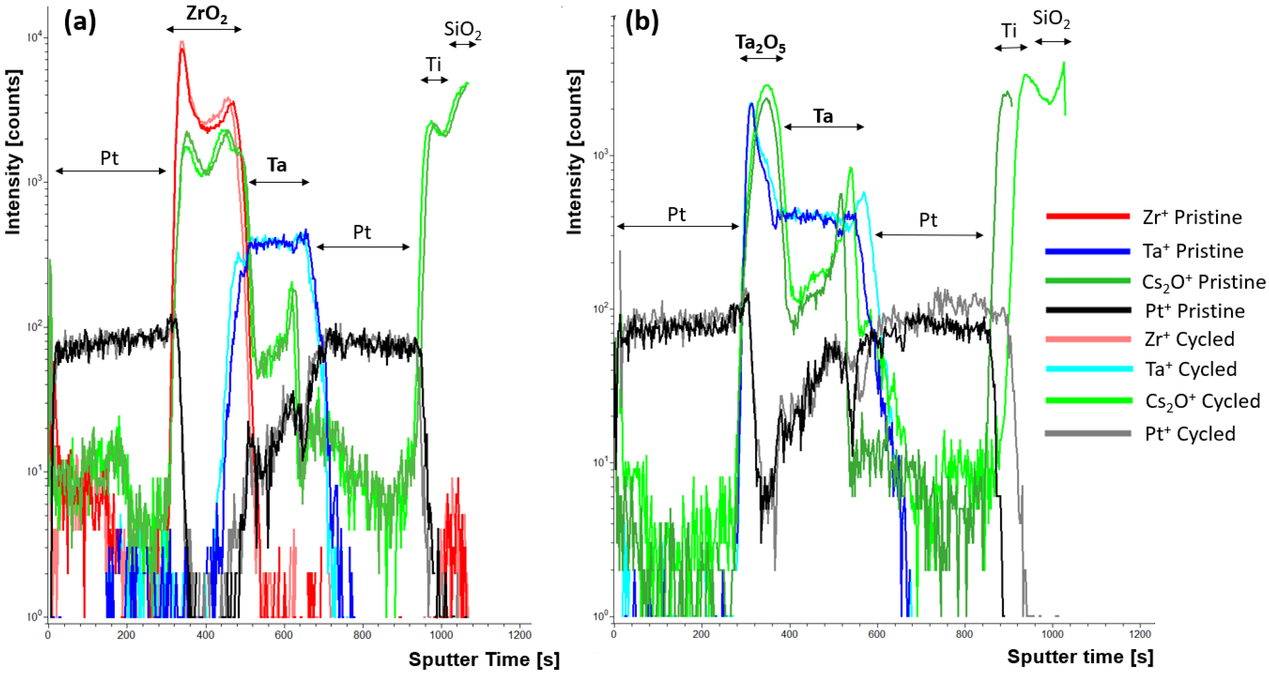
While the mechanisms proposed for the observed hysteresis are attributed to the PF conduction and trap-assisted tunneling, to elucidate whether ionic motion was participating in the observed wake-up behavior observed in the ZrO
2 and Ta
2O
5 devices, TOF-SIMS depth profiles were performed on pristine devices and compared to devices after 25 measurement cycles. The ToF-SIMS depth profiles, shown in
Figure 7a, show shifts in Cs
2O
+ (surrogate for oxygen), Ta
+ and Zr
+ signals at the top Pt/ZrO
2 and Ta/ZrO
2 interfaces after cycling the device 25×. This suggests that there is some oxygen motion within the active layer during this wake-up period. The corresponding current-voltage cycling can be found in
Figure S12. The relevant signals normalized to the total signal are shown in
Figures S13 and S14 for the ZrO
2 and Ta
2O
5 devices, respectively. In the ZrO
2 device, oxygen can be seen to migrate in the ZrO
2 layer toward the bottom Ta layer. This migration is tracked using the Cs
2O
+ signal. As Doolittle et al. [
15] suggests, a highly charged layer generated at the electrode/active layer interface can result in increased tunnel injection during the during the positive sweep. Thus, the observed oxygen buildup observed at the ZrO
2/Ta interface could be inducing a highly charged layer or oxidizing the interface and thus locally increasing the electric field, which is consistent with the observed maximum current increase observed with increasing cycle number during positive poling. Tracking the Zr
+ signal shows a concomitant migration of Zr
+ at the Ta interface. This could be due to slight densification during the wake-up or demixing at the ZrO
2/Ta interface. In the Ta
2O
5 devices shown in
Figure 7b, minimal change is observed in the Cs
2O
+ signal and the Ta
+ signal. This is likely due to the smaller fields required to operate and wake the device up. The spike in Ta
+ count at the Pt/Ta
2O
5 interface is attributed to the matrix effect generating increased ionization rates at interfaces due to variation in bonding compared to the bulk of the film [
30,
31]. It is interesting that there is a slight expansion of the Ta layer observed, along with a buildup of oxygen bottom Ta/Pt interface (though note that the scale is logarithmic, so a low concentration relative the Ta
2O
5 layer concentration). These changes at the Ta/Pt interface are not expected to substantially change the conduction mechanism in the Ta
2O
5 devices as a majority of the voltage drop should be across the Ta
2O
5 layer. The shift in Pt
+ at in the Ta
2O
5 device is attributed to thickness variation across the sample in the bottom Pt layer and is not expected to affect device performance.


 ,
, 

