
Investigation of Gas Sensing Performance of CuO/Cu2O Thin Films as a Function of Au-NP Size for CO, CO2, and Hydrocarbons Mixtures

 , ,
, ,
Abstract

1. Introduction
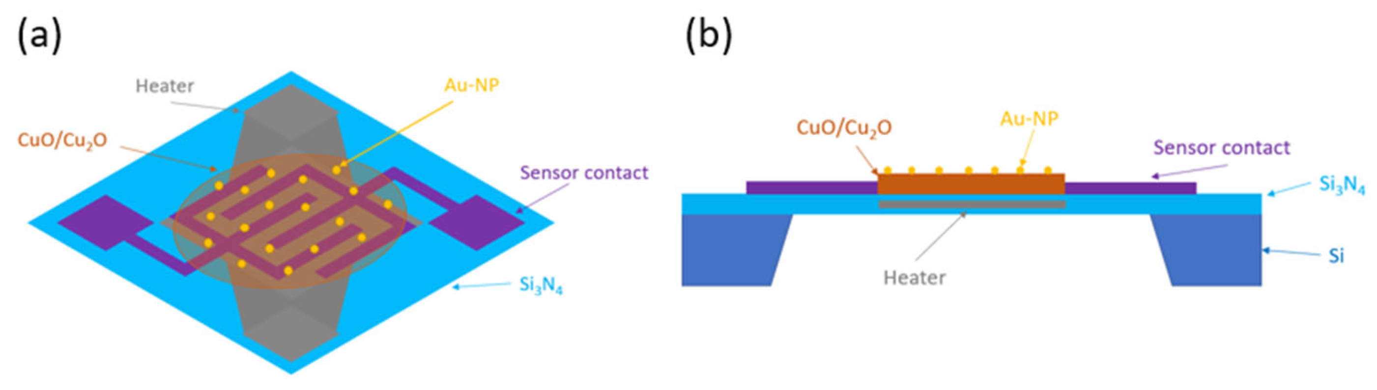
2. Sensor Fabrication
3. Synthesis of Au-Nanoparticles
4. Sensor Functionalization and Sensor Device
5. Sensor Characterisation
6. Results
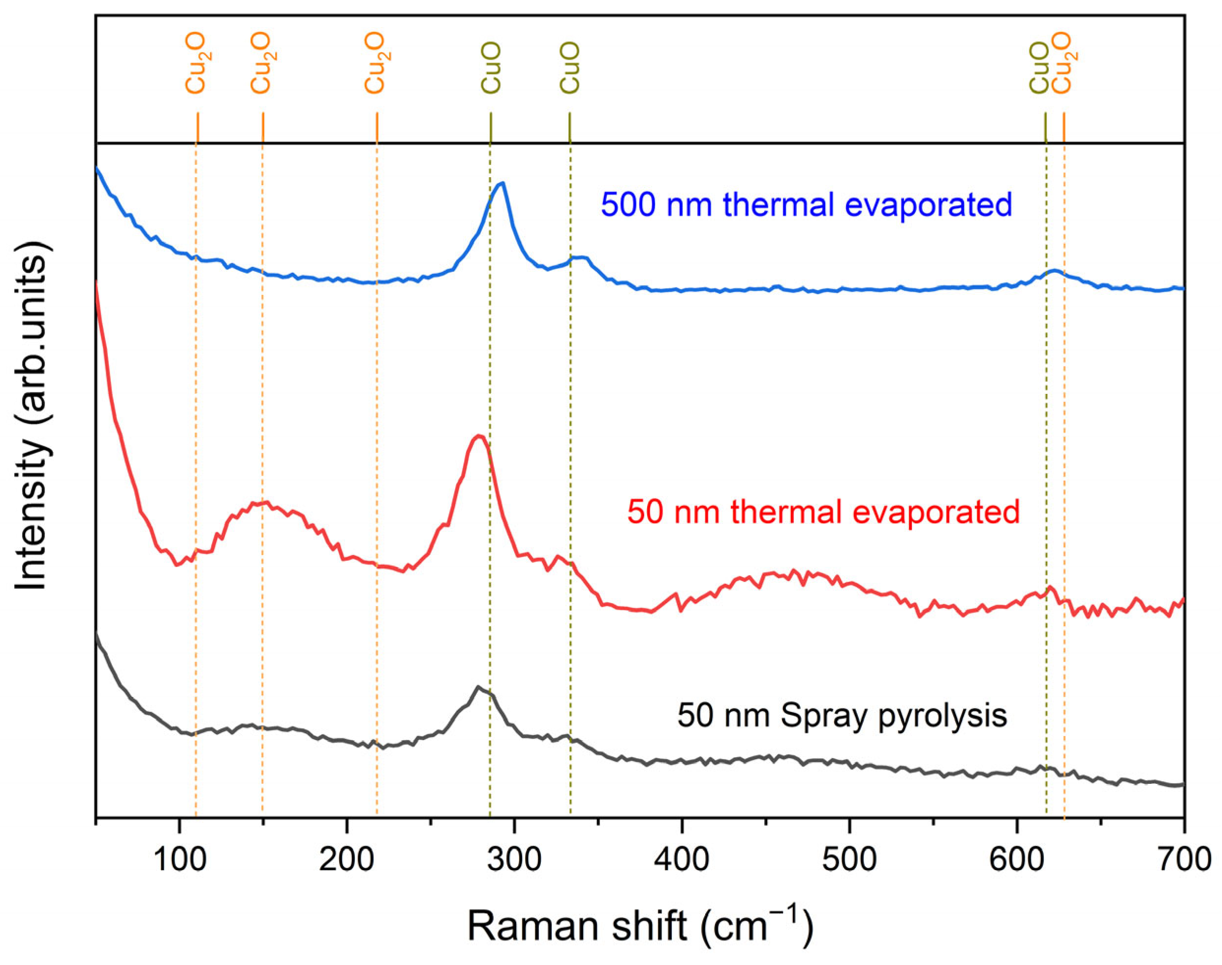
6.1. Raman Investigations
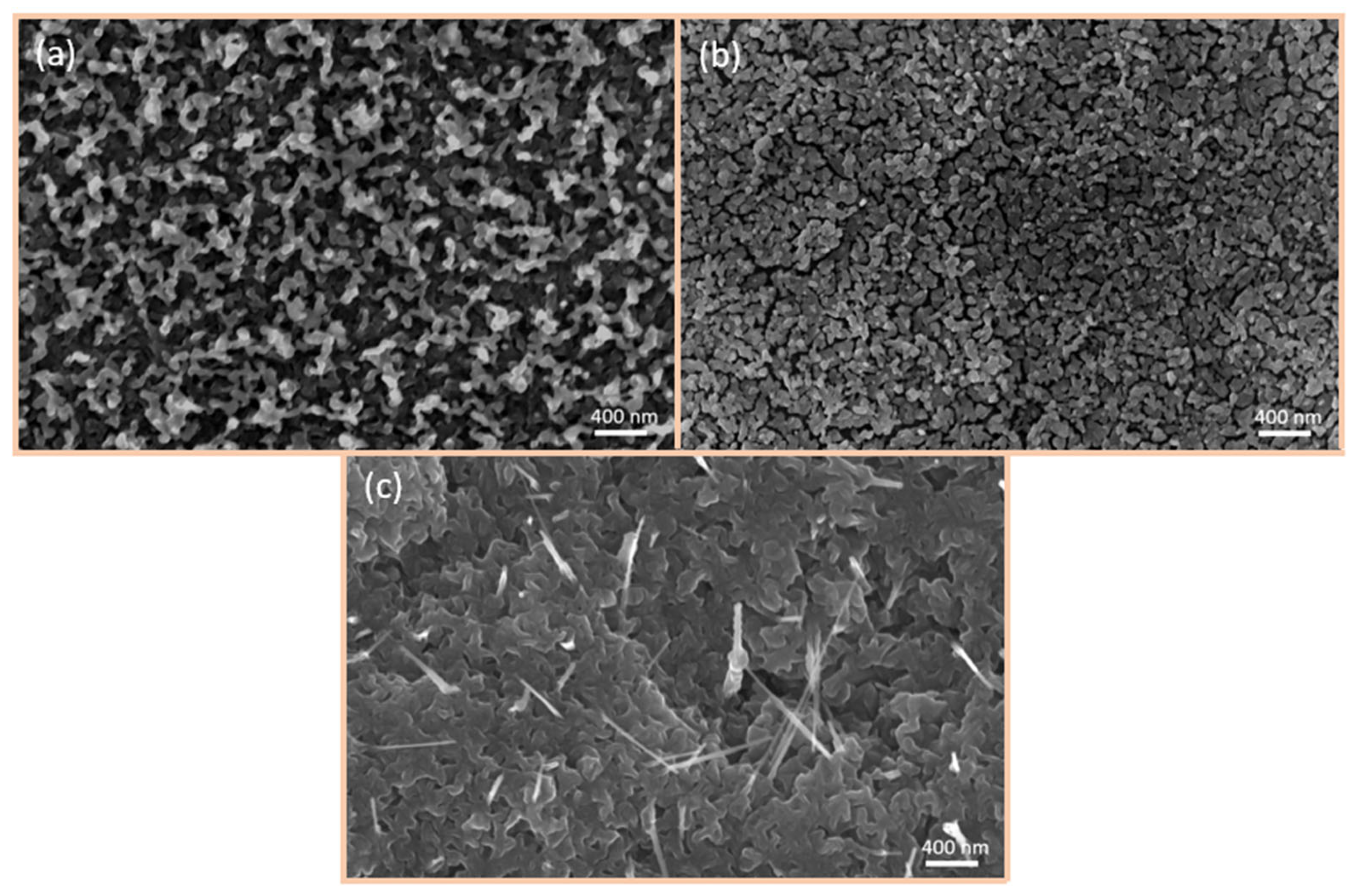
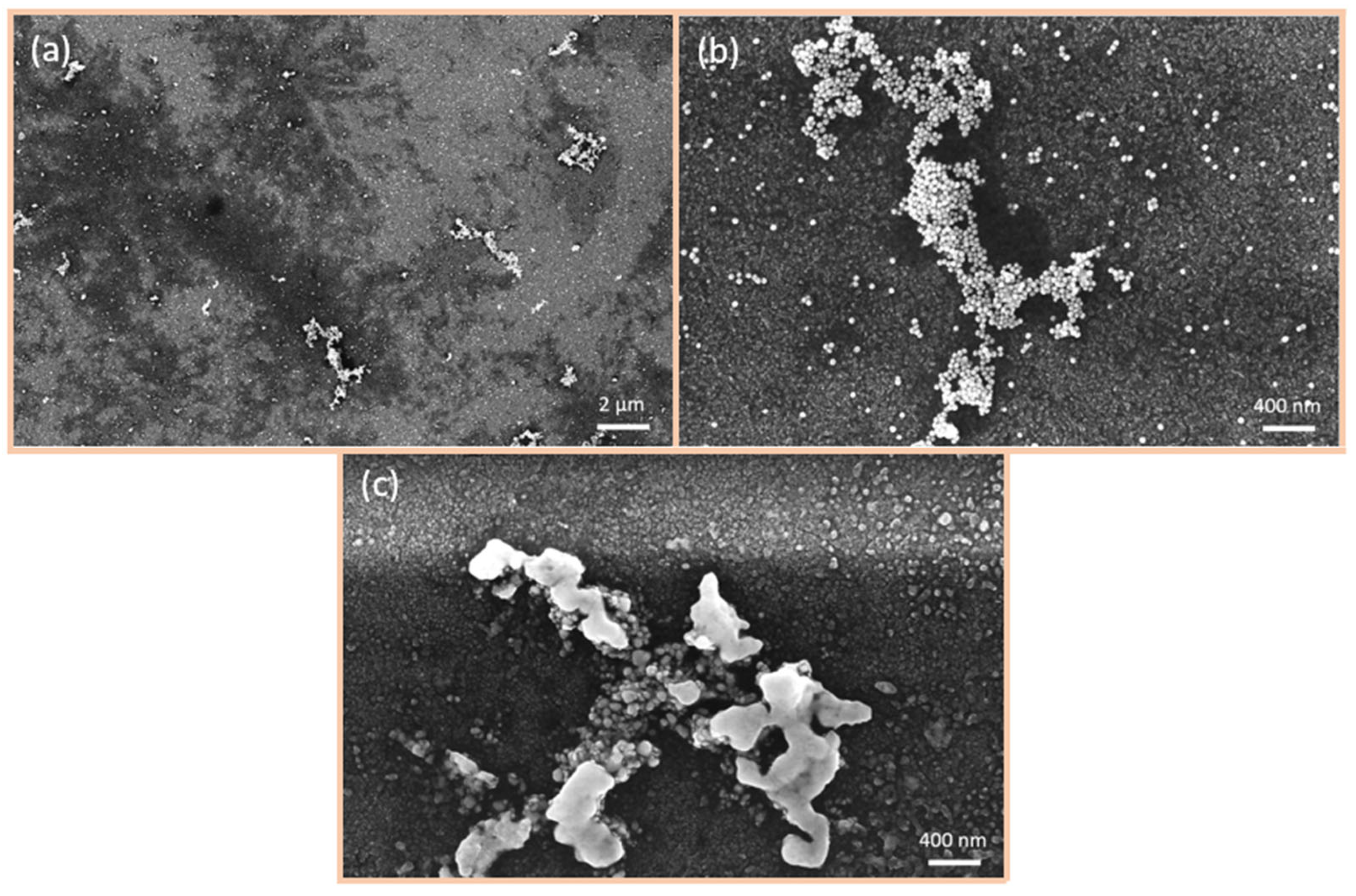
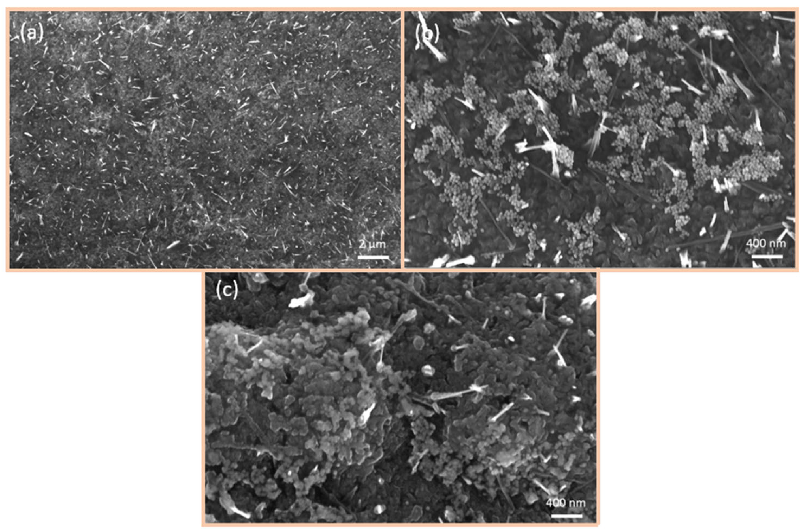
6.2. SEM Investigations
6.3. Sensor Performance
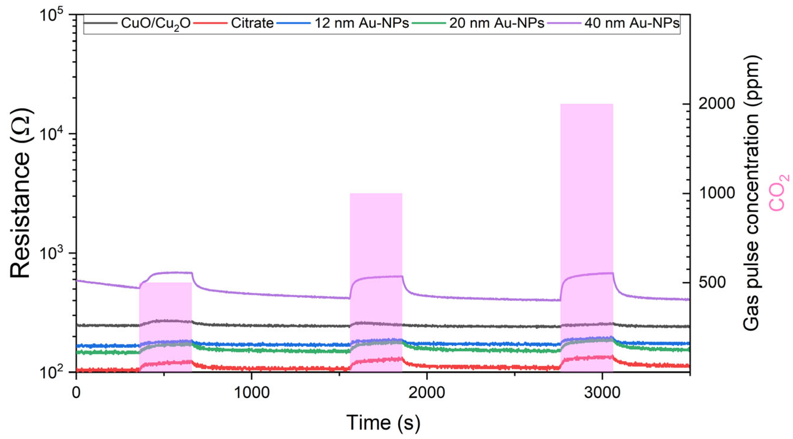
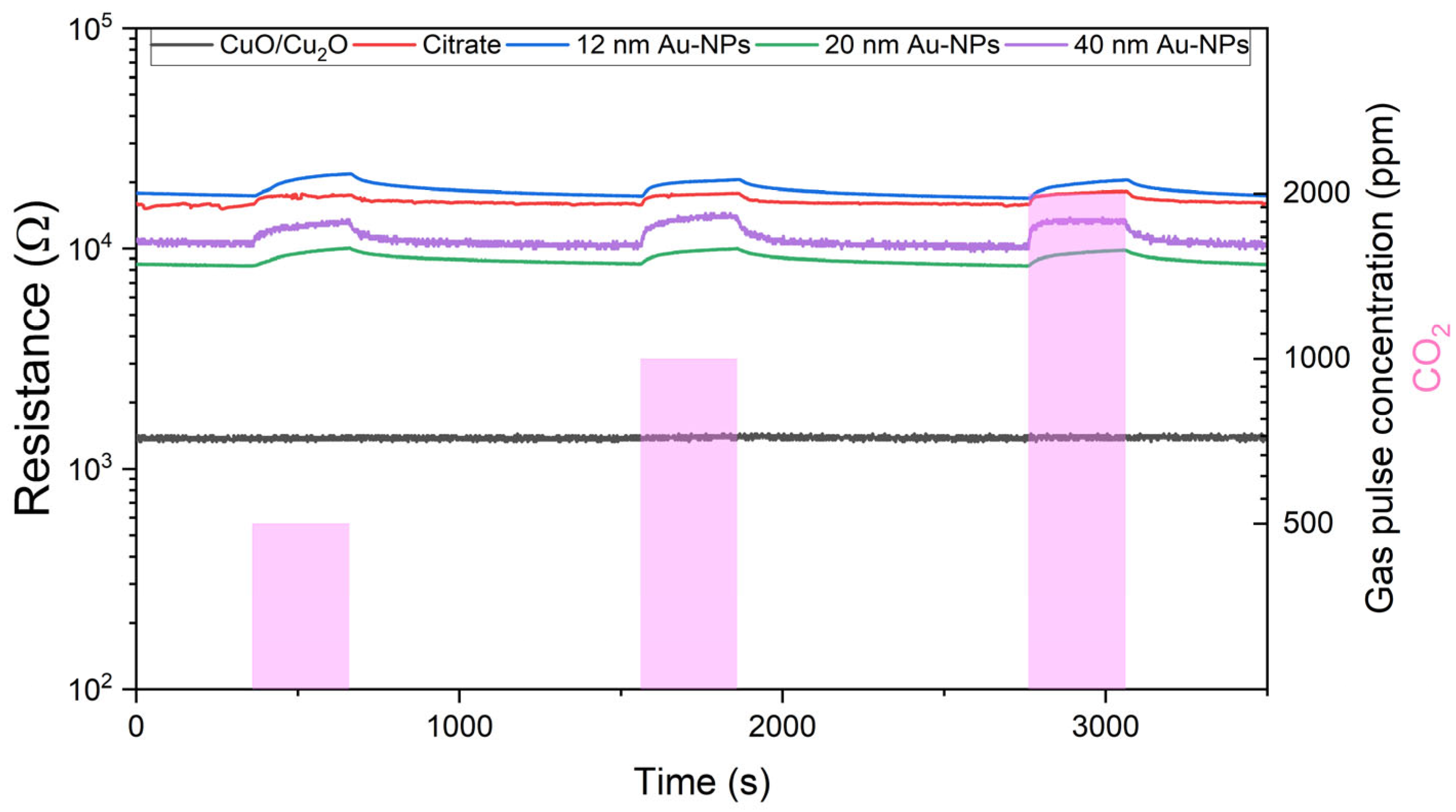
6.3.1. Resistance Measurements
6.3.2. Response and Recovery Time
6.3.3. Sensor Response
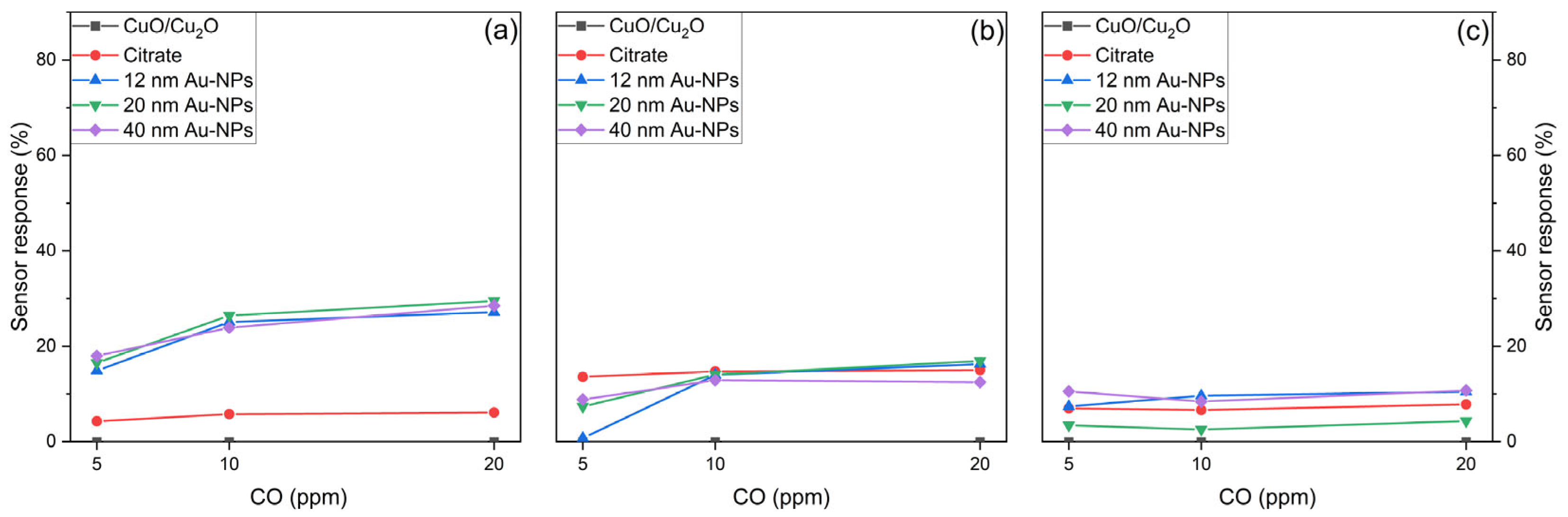
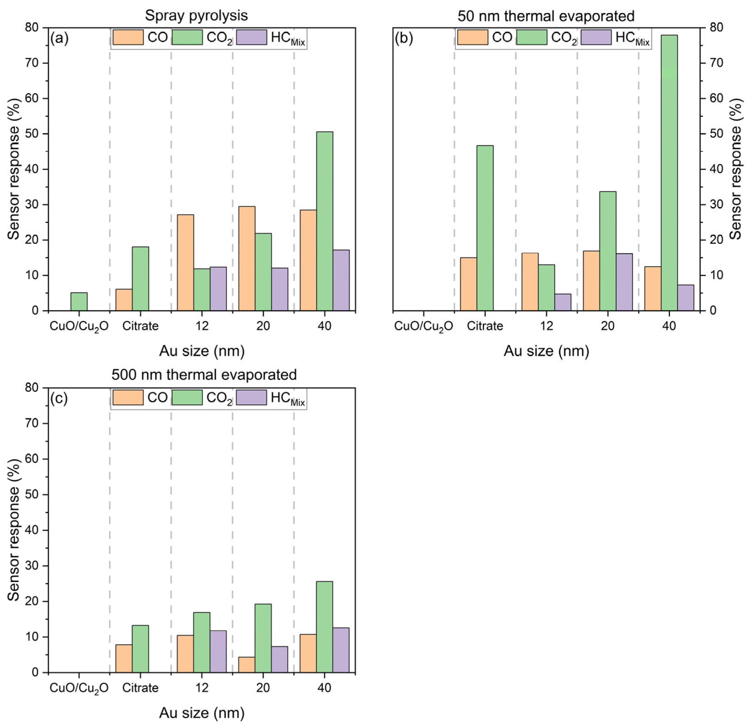
- Sensing performance for CO
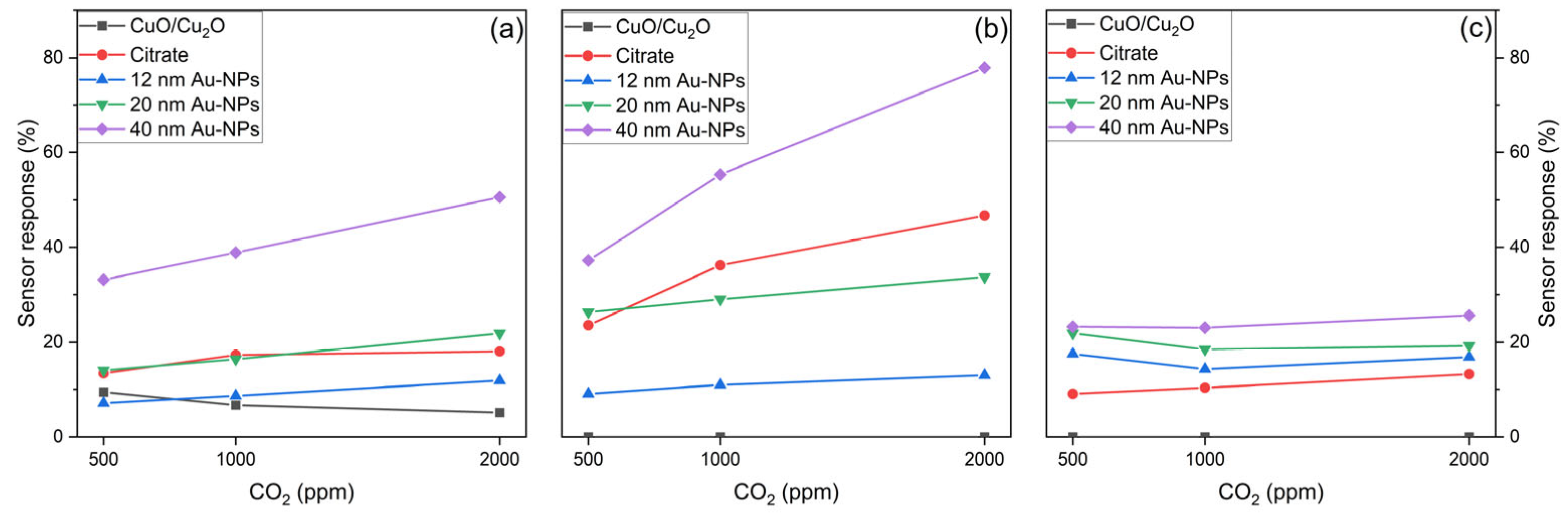
- Sensing performance for CO2
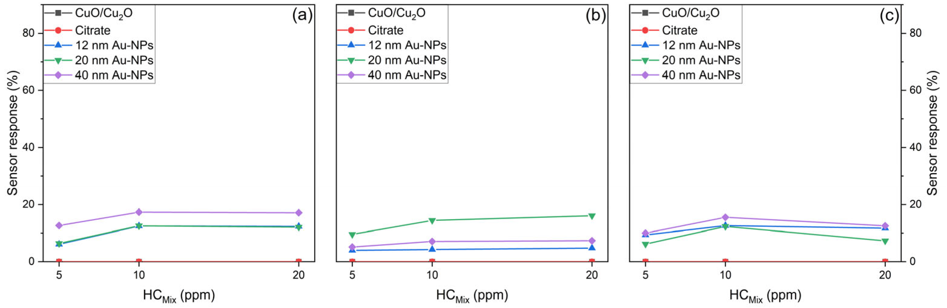
- Sensing performance for HCMix
6.3.4. Comparison of Sensor Response
7. Summary and Discussion
Author Contributions
Funding
Data Availability Statement
Acknowledgments
Conflicts of Interest
References
- Neri, G. First Fifty Years of Chemoresistive Gas Sensors. Chemosensors 2015, 3, 1–20. [Google Scholar] [CrossRef]
- Krishna, K.G.; Parne, S.; Pothukanuri, N.; Kathirvelu, V.; Gandi, S.; Joshi, D. Nanostructured metal oxide semiconductor-based gas sensors: A comprehensive review. Sens. Actuators A Phys. 2022, 341, 113578. [Google Scholar] [CrossRef]
- Xu, M.; Tian, W.; Lin, Y.; Xu, Y.; Tao, J. Development of a Compact NDIR CO2 Gas Sensor for a Portable Gas Analyzer. Micromachines 2024, 15, 1203. [Google Scholar] [CrossRef] [PubMed]
- Khorramifar, A.; Karami, H.; Lvova, L.; Kolouri, A.; Łazuka, E.; Piłat-Rożek, M.; Łagód, G.; Ramos, J.; Lozano, J.; Kaveh, M.; et al. Environmental Engineering Applications of Electronic Nose Systems Based on MOX Gas Sensors. Sensors 2023, 23, 5716. [Google Scholar] [CrossRef] [PubMed]
- Kulkarni, S.; Ghosh, R. Investigation of Surface Affinity and Desorption Kinetics of Mixture of Volatile Organic Compounds on CuO-Based Resistive Gas Sensors. IEEE Sens. Lett. 2024, 8, 1–4. [Google Scholar] [CrossRef]
- Steinhauer, S. Gas Sensors Based on Copper Oxide Nanomaterials: A Review. Chemosensors 2021, 9, 51. [Google Scholar] [CrossRef]
- Sihag, S.; Dahiya, R.; Rani, S.; Berwal, P.; Jatrana, A.; Sisodiya, A.K.; Sharma, A.; Kumar, V. Low ppm NO2 detection through advanced ultrasensitive copper oxide gas sensor. Discov. Nano 2024, 19, 107. [Google Scholar] [CrossRef]
- Duan, X.; Jiang, Y.; Liu, B.; Duan, Z.; Zhang, Y.; Yuan, Z.; Tai, H. Enhancing the carbon dioxide sensing performance of LaFeO3 by Co doping. Sens. Actuators B Chem. 2024, 402, 135136. [Google Scholar] [CrossRef]
- Maier, C.; Egger, L.; Köck, A.; Reichmann, K. A Review of Gas Sensors for CO2 Based on Copper Oxides and Their Derivatives. Sensors 2024, 24, 5469. [Google Scholar] [CrossRef]
- Dulmaa, A.; Vrielinck, H.; Khelifi, S.; Depla, D. Sputter deposition of copper oxide films. Appl. Surf. Sci. 2019, 492, 711–717. [Google Scholar] [CrossRef]
- Mahana, D.; Mauraya, A.K.; Singh, P.; Muthusamy, S.K. Evolution of CuO thin films through thermal oxidation of Cu films prepared by physical vapour deposition techniques. Solid State Commun. 2023, 366–367, 115152. [Google Scholar] [CrossRef]
- Bellal, Y.; Bouhank, A.; Serrar, H.; Tüken, T.; Sığırcık, G. A Copper Oxide (CuO) Thin Films Deposited by Spray Pyrolysis Method. MATEC Web Conf. 2019, 253, 3002. [Google Scholar] [CrossRef]
- Krishna, M.G.; Murthy, M.N.; Sreelatha, C.J.; Kumar, K.R.; Chandrakala, G. Sol-Gel Synthesized Copper Oxide (Cuo) Nanoparticles And Their Photocatalysts And Antibacterial Applications. Rasayan J. Chem. 2023, 16, 2256–2260. [Google Scholar] [CrossRef]
- Salim, E.; Abaas, R.; Mahdi, R. A sight of view on hydrothermal synthesis of copper oxide. Eng. Technol. J. 2023, 41, 592–602. [Google Scholar] [CrossRef]
- Maier, C.; Egger, L.; Köck, A.; Reichmann, K. Investigation of the Influence of Adhesion Layers on the Gas Sensing Performance of CuO/Cu2O Thin Films. Chemosensors 2025, 13, 80. [Google Scholar] [CrossRef]
- Maier, C.; Leitgeb, V.; Egger, L.; Köck, A. Size-Dependent Thresholds in CuO Nanowires: Investigation of Growth from Microstructured Thin Films for Gas Sensing. Nanomaterials 2024, 14, 5469. [Google Scholar] [CrossRef]
- John, R.A.B.; Ruban, K.A. A review on resistive-based gas sensors for the detection of volatile organic compounds using metal-oxide nanostructures. Inorg. Chem. Commun. 2021, 133, 108893. [Google Scholar] [CrossRef]
- Abideen, Z.U.; Kim, J.-H.; Lee, J.-H.; Kim, J.-Y.; Mirzaei, A.; Kim, H.W.; Kim, S.S. Electrospun Metal Oxide Composite Nanofibers Gas Sensors: A Review. J. Korean Ceram. Soc. 2017, 54, 366–379. [Google Scholar] [CrossRef]
- Navale, S.; Shahbaz, M.; Mirzaei, A.; Kim, S.S.; Kim, H.W. Effect of Ag Addition on the Gas-Sensing Properties of Nanostructured Resistive-Based Gas Sensors: An Overview. Sensors 2021, 21, 6454. [Google Scholar] [CrossRef]
- Velmathi, G.; Mohan, S.; Henry, R. Analysis of Factors for Improving Functionality of Tin Oxide Gas Sensor. IETE Tech. Rev. 2016, 33, 122–129. [Google Scholar] [CrossRef]
- Egger, L.; Sosada-Ludwikowska, F.; Steinhauer, S.; Singh, V.; Grammatikopoulos, P.; Köck, A. SnO2-Based CMOS-Integrated Gas Sensor Optimized by Mono-, Bi-, and Trimetallic Nanoparticles. Chemosensors 2025, 13, 59. [Google Scholar] [CrossRef]
- Korotcenkov, G.; Brinzari, V.; Gulina, L.B.; Cho, B.K. The influence of gold nanoparticles on the conductivity response of SnO2-based thin film gas sensors. Appl. Surf. Sci. 2015, 353, 793–803. [Google Scholar] [CrossRef]
- Wimmer-Teubenbacher, R.; Sosada-Ludwikowska, F.; Travieso, B.; Defregger, S.; Tokmak, O.; Niehaus, J.; Deluca, M.; Köck, A. CuO Thin Films Functionalized with Gold Nanoparticles for Conductometric Carbon Dioxide Gas Sensing. Chemosensors 2018, 6, 56. [Google Scholar] [CrossRef]
- Maier, C.; Egger, L.; Köck, A.; Becker, S.; Niehaus, J.S.; Reichmann, K. Investigation of the gas-sensing performance of CuO sensors functionalized with different stabilized Au nanoparticles. J. Sens. Sens. Syst. 2025, 14, 55–65. [Google Scholar] [CrossRef]
- Lee, J.-S.; Katoch, A.; Kim, J.-H.; Kim, S.S. Effect of Au nanoparticle size on the gas-sensing performance of p-CuO nanowires. Sens. Actuators B Chem. 2016, 222, 307–314. [Google Scholar] [CrossRef]
- Zhussupbekova, A.; Zhussupbekov, K.; Verre, R.; Caffrey, D.; Shiel, K.; Shvets, I.V.; Fleischer, K. An In Situ Study of Precursor Decomposition via Refractive Index Sensing in p-Type Transparent Copper Chromium Oxide. Chem. Mater. 2022, 34, 3020–3027. [Google Scholar] [CrossRef]
- Oliveira, A.E.F.; Pereira, A.C.; Resende, M.A.C.; Ferreira, L.F. Gold Nanoparticles: A Didactic Step-by-Step of the Synthesis Using the Turkevich Method, Mechanisms, and Characterizations. Analytica 2023, 4, 250–263. [Google Scholar] [CrossRef]
- Maier, C.; Egger, L.; Köck, A.; Becker, S.; Niehaus, J. OT5. 154—Gas Sensing Performance of CuO Sensors Functionalized with Different Stabilized Au-NP. In Proceedings of the EUROSENSORS XXXVI, Debrecen, Hungary, 1–4 September 2024; AMA Service GmbH, Von-Münchhausen-Str. 49, 31515 Wunstorf. 2024; pp. 119–120. [Google Scholar]
- Yevdokymenko, V.Y.; Dobrozhan, O.; Pshenychnyi, R.; Opanasyuk, A.; Gnatenko, Y.; Bukivskii, A.; Bukivskij, P.; Gamernyk, R.; Klymov, O.; Muñoz-Sanjosé, V.; et al. The effect of annealing treatment on the structural and optical properties of nanostructured CuxO films obtained by 3D printing. Mater. Sci. Semicond. Process. 2023, 161, 107472. [Google Scholar] [CrossRef]
- Debbichi, L.; Marco de Lucas, M.C.; Pierson, J.F.; Krüger, P. Vibrational Properties of CuO and Cu4O3 from First-Principles Calculations, and Raman and Infrared Spectroscopy. J. Phys. Chem. C 2012, 116, 10232–10237. [Google Scholar] [CrossRef]
- Purusottam-Reddy, B.; Sivajee-Ganesh, K.; Jayanth-Babu, K.; Hussain, O.M.; Julien, C.M. Microstructure and supercapacitive properties of rf-sputtered copper oxide thin films: Influence of O2/Ar ratio. Ionics 2015, 21, 2319–2328. [Google Scholar] [CrossRef]
- Murthy, P.S.; Venugopalan, V.P.; Das, D.A.; Dhara, S.; Pandiyan, R.; Tyagi, A.K. Antibiofilm activity of nano sized CuO. In Proceedings of the International Conference on Nanoscience, Engineering and Technology (ICONSET 2011), Chennai, India, 28–30 November 2011; IEEE: Piscataway, NJ, USA, 2011; pp. 580–583, ISBN 978-1-4673-0074-2. [Google Scholar]
- Robin, C.; Neha, K.; Amit, K.; Banerjee, D. Chemical Synthesis of Copper Oxide Nanoparticles Study of its Optical and Electrical Properties. Int. J. Eng. Res. Technol. 2020, 9, 258–261. [Google Scholar] [CrossRef]
- Xu, J.F.; Ji, W.; Shen, Z.X.; Li, W.S.; Tang, S.H.; Ye, X.R.; Jia, D.Z.; Xin, X.Q. Raman spectra of CuO nanocrystals. J. Raman Spectrosc. 1999, 30, 413–415. [Google Scholar] [CrossRef]
- Mohamed, S.H.; Al-Mokhtar, K.M. Characterization of Cu2O/CuO nanowire arrays synthesized by thermal method at various temperatures. Appl. Phys. A 2018, 124, 493. [Google Scholar] [CrossRef]
- Sumangala, T.P.; Thimont, Y.; Baco-Carles, V.; Presmanes, L.; Bonningue, C.; Pasquet, I.; Tailhades, P.; Barnabé, A. Study on the effect of cuprite content on the electrical and CO2 sensing properties of cuprite-copper ferrite nanopowder composites. J. Alloys Compd. 2017, 695, 937–943. [Google Scholar] [CrossRef]
- IEEE Reliability Society. In Proceedings of the 2nd International Symposium on Physics and Technology of Sensors (ISPTS 2015). Pune, India, 7–10 March 2015; IEEE: Piscataway, NJ, USA, 2015. ISBN 9781467380195. [Google Scholar]
- Tanvir, N.B.; Yurchenko, O.; Laubender, E.; Pohle, R.; Sicard, O.; Urban, G. Zinc peroxide combustion promoter in preparation of CuO layers for conductometric CO2 sensing. Sens. Actuators B Chem. 2018, 257, 1027–1034. [Google Scholar] [CrossRef]
- Sun, Y.-F.; Liu, S.-B.; Meng, F.-L.; Liu, J.-Y.; Jin, Z.; Kong, L.-T.; Liu, J.-H. Metal oxide nanostructures and their gas sensing properties: A review. Sensors 2012, 12, 2610–2631. [Google Scholar] [CrossRef]
- Chang, J.F.; Kuo, H.H.; Leu, I.C.; Hon, M.H. The effects of thickness and operation temperature on ZnO: Al thin film CO gas sensor. Sens. Actuators B 2002, 84, 258–264. [Google Scholar] [CrossRef]


| Response Time [s] | ||||
|---|---|---|---|---|
| Method | Citrate | 12 nm Au-NPs | 20 nm Au-NPs | 40 nm Au-NPs |
| Spray pyrolysis of 50 nm | 32.4 | 70.2 | 62.1 | 66.7 |
| Thermal evaporation of 50 nm | 87.5 | 37.3 | 99.8 | 107.9 |
| Thermal evaporation of 500 nm | 49.5 | 146.7 | 125.9 | 40.6 |
| Recovery Time [s] | ||||
| Method | Citrate | 12 nm Au-NPs | 20 nm Au-NPs | 40 nm Au-NPs |
| Spray pyrolysis of 50 nm | 96.9 | 38.5 | 84.1 | 61.5 |
| Thermal evaporation of 50 nm | 128.8 | 65.9 | 133.3 | 129.7 |
| Thermal evaporation of 500 nm | 137.4 | 199.5 | 184.2 | 135.31 |
| Morphology | Method | Operating Temperature (°C) | Relative Humidity (%) | CO2 (ppm) | Sensor Response | References |
|---|---|---|---|---|---|---|
| CuO/CuFe2O4 Thick film | Co-precipitation (paste) | 350 | 0 | 5000 | 10% | [36] |
| SnO2/CuO with 0.5 wt% Ag Nanospheres | Hydrothermal process | 300 | Not defined | 10,000 | 72% | [37] |
| CuO-NPs with ZnO | Drop coating | 300 | 30 | 1000 | 12% | [38] |
| CuO with Au | Drop coating | 300 | 50 | 2000 | 78% | This work |
Disclaimer/Publisher’s Note: The statements, opinions and data contained in all publications are solely those of the individual author(s) and contributor(s) and not of MDPI and/or the editor(s). MDPI and/or the editor(s) disclaim responsibility for any injury to people or property resulting from any ideas, methods, instructions or products referred to in the content. |
© 2025 by the authors. Licensee MDPI, Basel, Switzerland. This article is an open access article distributed under the terms and conditions of the Creative Commons Attribution (CC BY) license (https://creativecommons.org/licenses/by/4.0/).
Share and Cite
Maier, C.; Egger, L.; Köck, A.; Becker, S.; Niehaus, J.S.; Reichmann, K. Investigation of Gas Sensing Performance of CuO/Cu2O Thin Films as a Function of Au-NP Size for CO, CO2, and Hydrocarbons Mixtures. Nanomaterials 2025, 15, 705. https://doi.org/10.3390/nano15100705
Maier C, Egger L, Köck A, Becker S, Niehaus JS, Reichmann K. Investigation of Gas Sensing Performance of CuO/Cu2O Thin Films as a Function of Au-NP Size for CO, CO2, and Hydrocarbons Mixtures. Nanomaterials. 2025; 15(10):705. https://doi.org/10.3390/nano15100705
Chicago/Turabian StyleMaier, Christian, Larissa Egger, Anton Köck, Sören Becker, Jan Steffen Niehaus, and Klaus Reichmann. 2025. "Investigation of Gas Sensing Performance of CuO/Cu2O Thin Films as a Function of Au-NP Size for CO, CO2, and Hydrocarbons Mixtures" Nanomaterials 15, no. 10: 705. https://doi.org/10.3390/nano15100705
APA StyleMaier, C., Egger, L., Köck, A., Becker, S., Niehaus, J. S., & Reichmann, K. (2025). Investigation of Gas Sensing Performance of CuO/Cu2O Thin Films as a Function of Au-NP Size for CO, CO2, and Hydrocarbons Mixtures. Nanomaterials, 15(10), 705. https://doi.org/10.3390/nano15100705