Article

Synthesis and Characterization of SiO2-Based Graphene Nanoballs Using Copper-Vapor-Assisted APCVD for Thermoelectric Application

by
Nurkhaizan Zulkepli
1,2,
Jumril Yunas
1,*,
Muhammad Aniq Shazni Mohammad Haniff
1,
Dedi
3,
Mohamad Shukri Sirat
1,
Muhammad Hilmi Johari
1,
Nur Nasyifa Mohd Maidin
1,
Aini Ayunni Mohd Raub
1 and
Azrul Azlan Hamzah
1,*
1
Institute of Microengineering and Nanoelectronic (IMEN), Universiti Kebangsaan Malaysia (UKM), Bangi 46300, Selangor, Malaysia
2
Centre of Foundation Studies, Universiti Teknologi MARA, Cawangan Selangor, Kampus Dengkil, Dengkil 43800, Selangor, Malaysia
3
Research Center for Advanced Materials, National Research and Innovation Agency (BRIN), South Tangerang 15314, Banten, Indonesia
*
Authors to whom correspondence should be addressed.
Nanomaterials 2024, 14(7), 618; https://doi.org/10.3390/nano14070618
Submission received: 31 May 2023 / Revised: 23 June 2023 / Accepted: 10 July 2023 / Published: 1 April 2024

Abstract

:
This study describes a method by which to synthesize SiO2-based graphene nanoballs (SGB) using atmospheric pressure chemical vapor deposition (APCVD) with copper vapor assistance. This method should solve the contamination, damage, and high costs associated with silica-based indirect graphene synthesis. The SGB was synthesized using APCVD, which was optimized using the Taguchi method. Multiple synthesis factors were optimized and investigated to find the ideal synthesis condition to grow SGB for thermoelectric (TE) applications. Raman spectra and FESEM-EDX reveal that the graphene formed on the silicon nanoparticles (SNP) is free from copper. The prepared SGB has excellent electrical conductivity (75.0 S/cm), which shows better results than the previous report. Furthermore, the SGB nanofillers in bismuth telluride (Bi2Te3) nanocomposites as TE materials exhibit a significant increment in Seebeck coefficients (S) compared to the pure Bi2Te3 sample from 109 to 170 μV/K at 400 K, as well as electrical resistivity decrement. This approach would offer a simple strategy to improve the TE performance of commercially available TE materials, which is critical for large-scale industrial applications.

1. Introduction

It is becoming more critical to comprehend the synthesis and characteristics of low-dimensional carbon nanomaterials such as graphene, carbon nanotubes (CNTs), and fullerenes on semiconductor materials owing to their synergetic effects [1,2,3]. The combination of these heterogeneous materials has broad potential applications, from environmental studies and construction materials to portable electronic devices, highlighting the tremendous potential implementation of graphene-based nanocomposite for future power generation [4] On top of that, graphene, CNTs, fullerenes, and their derivatives have garnered worldwide attention in the past decade, offering enormous potential in biosensors [5,6,7], flexible pressure sensors [8], nanocomposite electrodes [9,10], tunable absorbers [11,12], and photocatalysts [13,14], as well as energy generation [15].
Interest in the direct growth of graphene on semiconductors has been intriguing in recent years due to the impressive improvements of graphene–semiconductor interfaces, which have contributed to synergetic effects in hybrid devices. As a result, researchers began investigating more innovative approaches for directly growing graphene on silicon surfaces, including via hydrothermal carbonization [16], pulsed laser ablation [17], and dispersion polymerization technique [18]. On the other hand, many research groups continue their work on graphene–silicon nanocomposites synthesis for lithium-ion batteries using spray pyrolysis [19] and high-energy ball milling [20].
Chen et al. [21] reported their study on growing high-quality polycrystalline graphene on quartz by chemical vapor deposition (CVD). By using this technique, no post-growth transfer procedure is required, while remaining compatible with existing silicon manufacturing processes. Despite the extensive research efforts to directly grow graphene on silicon surfaces, the primary obstacles remain the mass production of high-quality graphene with few or no impurities or defects and the ability to produce graphene with a large grain size at a reasonable cost [22].
After all, CVD is one of the most cost-effective and scalable techniques for producing graphene with high crystallinity [22]. In the CVD process, there are two types of total reaction pressure: low-pressure CVD (LPCVD) [23] and atmospheric-pressure CVD (APCVD). Pumping systems are eliminated in APCVD, making it an attractive solution for low-cost graphene synthesis [24]. CVD methods have been extensively investigated in the literature to synthesize graphene on SiO2, as shown in Table 1.
The use of metals as catalysts to effectively accelerate the decomposition of carbon sources, such as copper or nickel, is common. Vaporous copper atoms were evaporated from copper foil owing to the temperature commonly used in the annealing process (1000 °C) being slightly lower than the melting point of copper (1085 °C) [25]. The floating copper atoms operate as catalysts, allowing processes that would otherwise be prevented or hindered by a kinetic barrier in direct catalysis on oxide surfaces to proceed. The distant metal-catalyzed decomposition of hydrocarbons resulted in the formation of graphene with minimal defects and amorphous carbons. Providing optimal copper particles may result in more successful reactant collisions, boosting the efficiency of carbon feedstock decomposition in the gas phase.
As shown in Table 1, studies on graphene growth on SNP by the CVD method are lacking in the main literature. CVD methods were successfully exploited by Son et al. [26] to grow graphene on SNP. Graphene balls, consisting of 3D graphene layers surrounded by a SiOx nanoparticle, were reported, which are composed of graphene and silicon nanoparticles at its centre. They demonstrated the CVD process by utilizing a fixed-bed vertical tube reactor, demanding high precision and complexity. Recently, Zhao et al. [27] displayed graphene ball potential to improve the properties of stress sensors by dispersing it with graphene oxide through a one-step hydrothermal reduction self-assembly method.
Graphene synthesis by CVD is influenced by a wide range of variables, including temperature [28], pressure [29], and growth and annealing time [30]. As a result, setting up the ideal conditions with numerous factors is very time-consuming. Taguchi method offers a practical and systematic strategy for optimizing the system in such conditions [31]. Using orthogonal arrays, it is possible to analyze many variables with a short number of trials using an empirical method that combines mathematical and statistical approaches [32]. Primary parameters may thus be thoroughly studied, while secondary ones can be pushed aside. As a result, valuable time, energy, and resources may be spared. This method has been previously applied to optimize the production of graphene from various carbon sources such as methane, ethanol, plastic waste [33], and oil palm fibre [34].
Graphene has been widely utilized in electronic applications due to its high electrical conductivity (106 S/cm). TE materials should exhibit both high electrical conductivity and extremely low thermal conductivity values in order to qualify as good TE materials [35]. Integrating graphene with SNP preserves unique traits of the two-dimensional system, including a large specific surface area, elasticity, and high conductivity, while retaining excellent characteristics of SNP that are stable chemically and easy to modify, high-temperature resistance, and low cytotoxicity [36]. Applying uniform graphene coating to the SNP using a CVD method can potentially increase electrical conductivity while preserving low thermal conductivity values.
In this work, the SGB was directly grown on SiO2 nanopowder (SNP) and optimized using the Taguchi method for TE applications. The SGB was grown using the APCVD process with copper vapor as the catalyst. The key characteristic of the proposed method is hydrocarbon breakdown through floating metal catalysis. Then, the optimized SGB were uniformly mixed in TE material nanocomposites, and its effect on the TE properties was evaluated.
Table 1. Growth of graphene on SiO2 with the CVD method.
SiO2 SurfaceGasFlowPressureTemperatureGrowth TimeCatalystRef.
(sccm)(Torr)(°C)(min)
Flat substrateAr/H2/CH465:50:14Atmospheric1100180O2[21] 2011
Flat substrateAr/H2/CH4230:5:30Atmospheric100030Cu[37] 2012
Flat substrate 300 nmH2/CH420:305100030Cu[38] 2013
Flat substrate QuartzAr/H2/CH4100:20:5060–360950–11005Ni[25] 2014
Nanoparticles 20–30 nmCH450Atmospheric100060-[26] 2017
Flat substrate Si 500 μmH2/CH4100:50.007110060Cu[39] 2018
Nanoparticles 20–30 nmAr/CH4200:25Atmospheric100020-[27] 2019
Flat substrate 300 nmAr/CH3OH 0.15102030Cu[40] 2019
Flat substrate 300 nmH2/CH425:150.0000795060-[41] 2020
Nanoparticles 20–30 nmAr/H2/CH478:2:50Atmospheric100060CuThis work

2. Experimental Section

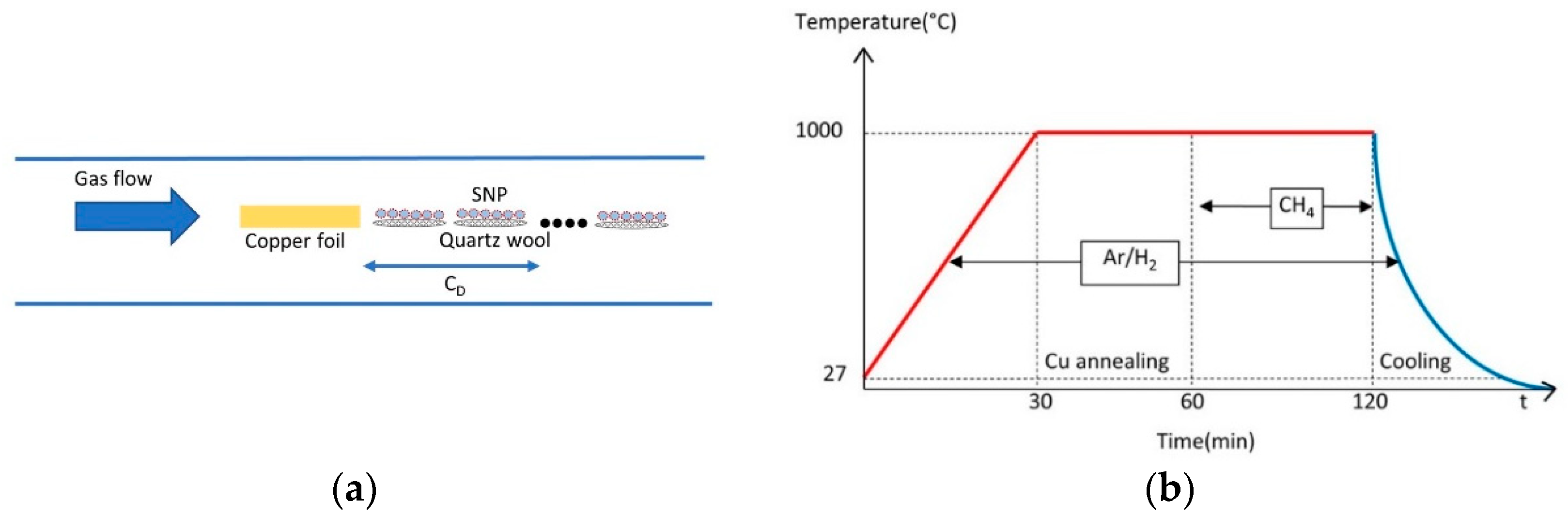
2.1. Graphene Growth

SGB was directly grown by using the APCVD method. Copper foil, CS (99.9% purity; 50 µm thick) varied in size, is initially sonicated in ethanol for 5 min, distilled water and IPA for 5 min, and lastly blown dry with nitrogen. The sample is immediately deposited on a porcelain boat and placed into a horizontal quartz tube with an inner diameter of 25.4 mm and a length of 800 mm at room temperature. Over 0.1 g of quartz wool (QW) and SNP (average diameter: 20–30 nm, Alfa Aesar, Haverhill, MA, USA) were placed into the same porcelain boat. The amount of SNP that was loaded into each batch was 0.01 g. The distance between copper foil and SNP, CD, was varied as shown in Figure 1a.
The quartz tube was sealed and purged with 80 sccm Ar/H2 for 30 min at atmospheric pressure before graphene growth could begin. This step was to flush the air from the quartz tube. While Ar/H2 gas flowed through the system, it was heated to 1000 °C at a ramping rate of 33 °C/min. The copper foil was annealed at 1000 °C for 30 min under Ar/H2 atmosphere to improve the copper grain size and to assure the elimination of native oxide and a smooth copper surface. Graphene was then grown by exposing it to an Ar/H2 and CH4 mixture at varying flow rates, ΦCH4, for 60 min. After growth, CH4 was shut off for the cooling step. As demonstrated in the growth protocol in Figure 1b, the samples were cooled from 1000 °C to room temperature in an Ar/H2 ambient.
A design of experiment (DOE) was conducted using Minitab 17 and the Taguchi Method to find the best synthesis parameter. This study evaluated the most relevant factors in the copper-catalysed synthesis of graphene. Three major parameters were reported to be the most influential: (1) methane flow rate (ΦCH4); (2) copper foil size (CS); and (3) copper distance (CD) [42]. The considered factors and their levels are shown in Table 2. Orthogonal arrays reduce the number of experiments by allowing randomized runs. The analysis aimed to obtain a low ID/IG ratio of SGB.

2.2. Characterization

The SGB was characterized using room temperature confocal micro-Raman imaging spectroscopy (DXR2Xi, Thermo Scientific, Waltham, MA, USA) to confirm the existence of graphene on SNP. The excitation wavelength was 532 nm, while the exposure time was 0.1 s. These measurements were conducted directly on the SGB. Three discrete points were investigated to characterize each sample and exclude potential spatial inhomogeneities correctly. The spectra were then averaged, normalized, and analyzed using spectroscopic analysis software. The morphological and cross-sectional views of the SGB were observed by field emission scanning electron microscopy (FESEM, Zeiss Merlin, Jena, Germany) and transmission electron microscopy (TEM, Thermo Scientific, Talos L120C, 120 kV). X-ray photoelectron spectroscopy (XPS) was carried out using an ULVAC-PHI Quantera II instrument with an Al-Kα monochromatic source (hv = 1486.6 eV) operating at 15 kV and 50 W. A Hall-effect measuring instrument (Ecopia, HMS-5300, Anyang, Republic of Korea) was utilized to characterize the electrical conductivity and charge mobility of the SGB for the electrical experiments. Electrical characterization was performed on a 0.5 cm × 0.5 cm sample size using a typical van der Pauw method under ambient air at 300 K by a Hall effect measurement system. The SGB was suspended in ethanol and was drop-casted on the surface of a glass substrate. The electrical resistivity, ρ, and Seebeck coefficient, S, of the SGB and TE material nanocomposites were tested using the LSR-4/800 (Linseis, Bayern, Germany) under low pressure (10−2 torr). Rectangular bars cut from 12 mm pellets with dimensions of 11.5 mm × 2.4 mm × 2.4 mm were tested at numerous temperature points ranging from room temperature to 500 K.

3. Results and Discussion

3.1. Optimization of SGB Synthesis Process

The important characteristic of the synthesized graphene layer is the ID/IG ratio, which is determined through Raman spectroscopy analysis on the sample. Initially, nine samples were synthesized using the copper-vapor-assisted APCVD method, and the extracted ID/IG ratio was calculated. As shown in Figure 2a, a small ID/IG ratio via Raman spectroscopy determines the good crystallinity of carbon-based materials as it indicates a low defect density [43].
To find the optimum process parameter, the ID/IG ratio by the nine synthesized samples was analyzed using Taguchi analysis. The experimental data were converted into a signal-to-noise ratio (SNR) to study each factor’s effect on SGB crystalline quality. In this work, the SNR was determined based on the “smaller is better” model in order to decrease the defect density in the graphitic lattice. The factor with the highest SNR value influences the considered output the most [32,44].
Figure 2b shows the mean of SNR ratios for each factor. According to the Taguchi analysis, the CD had the most significant impact on defectiveness in SGB, while ΦCH4 was the second most influential. The SGB synthesized under the conditions at ΦCH4 = 50 sccm, CS = 2 × 3 cm, and CD = 5 cm had the highest SNR, specifying the optimum process conditions for SGB synthesis. All these optimum values are indicated by the red circles. This study determines the best SGB synthesis factors for the lowest defect density.

3.2. Characterization of the Optimized SGB

3.2.1. Raman Analysis

The Raman spectra of SGB grown using the copper-vapor-assisted APCVD method are shown in Figure 3a. A combination of three prominent peaks can be seen in the Raman spectra of graphene: (1) The D-band, around 1350 cm−1, gives an excellent indication for measuring the level of disorder present in the sample; (2) the G-band, around 1580 cm−1, is related to the in-plane vibration of sp2-hybridized carbon atoms; and (3) the 2D band, roughly situated at 2680 cm−1, represents the thickness of graphene [45]. The analysis of the ID/IG ratio is a well-known method for evaluating the defect density of a graphene sample, whereas the I2D/IG ratio provides information on the number of layers present in a graphene sample. The method enables the differentiation of graphene from graphite and the assessment of the quality and thickness of graphene [46]. Defects in graphene may impair charge carrier mobility and hence electrical conductivity, which is detrimental to electronics applications [47].
In this work, the 2D band of SGB centred at 2684 cm−1. The ID/IG ratio indicates that the deposited SGB were mostly made of defective graphene layers. Defects are frequently associated with Stone–Wales defects, the presence of five or seven rings that alter the regular six-ring structure in a graphene lattice [47]. The I2D/IG ratio of the SGB indicates the development of graphene multilayers.
A series of experimental studies were conducted to determine the effect that copper played in the formation of graphene on SNP. For example, removing copper or replacing copper with Ni in the growth results in either amorphous carbon or a higher defect density of graphene on the SNP. As shown in Figure 3b, Ni is known to have a much higher melting point (mp = 1455 °C) than copper (mp = 1084 °C); hence, replacing copper ith Ni results in a higher defect density of graphene, as indicated by higher ID/IG ratios. Figure 3c shows that the exact process without copper foil produces no graphene. Compared to the process with the Cu catalyst, there are no clear 2D peaks observed. This observation proves that the distantly given copper vapor does indeed cause graphene growth, as shown in Figure 3c.
A high-temperature system is required for the growth process since evaporated copper is required to form graphene on SNP. Due to its high vapor pressure, copper foil rapidly evaporates to give off copper vapor at a growth temperature of 1000 °C [37]. Subsequently, copper vapor interacts with methane precursors adsorbed on the SNP, resulting in the nucleation of graphene formation in the lateral direction. The optimal ratio of copper vapor to methane gas (Cuvapor/CH4) seems to have contributed a significant role in the effective synthesis of SGB.

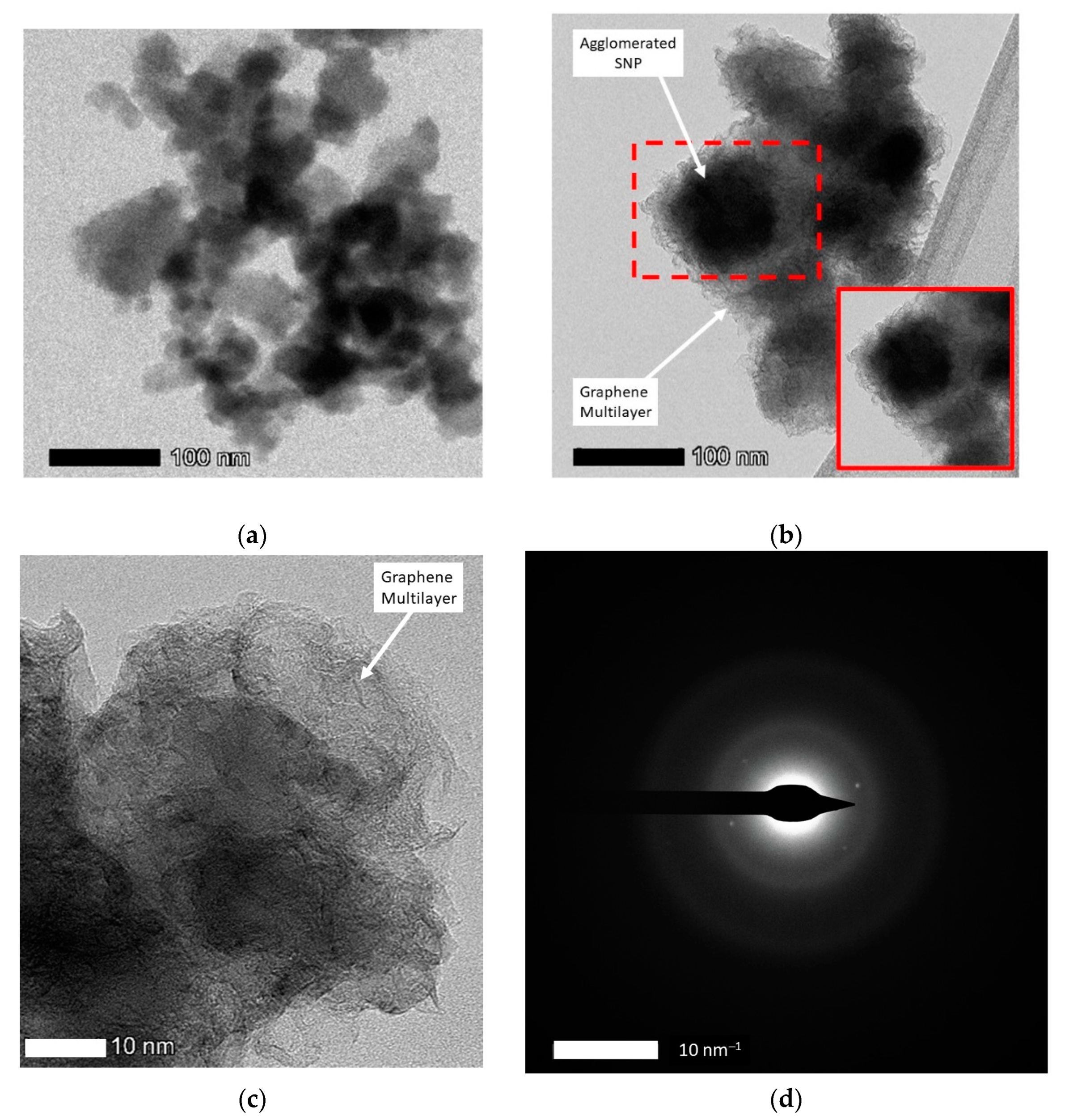
3.2.2. Morphology Analysis

Another essential requirement for the copper vapor-assisted CVD process is that the final SGB be copper-free. For this purpose, energy-dispersive X-ray (EDX) spectroscopy was employed to detect the amount of copper residue present in the graphene grown on SNP. To further ascertain that graphene growth is uniformly distributed on SNP, FESEM-EDX elemental mapping analysis of SGB has been carried out. Figure 4a shows FESEM images of SGB and the elemental maps of silicon, oxygen, and carbon, along with the corresponding overlay shown in Figure 4b. The SGB was composed of three elements: 45.1% of C; 23.6% of O; and 31.3% of Si, where C refers to graphene and O and Si correspond to SNP. These images reveal that graphene is uniformly distributed on SNP. Neither the EDX nor the FESEM-EDX elemental mapping analysis of SGB showed the presence of copper residues within the detection limit. This finding suggests that no copper-related chemical species are detected in the samples, suggesting that the copper acts as a catalyst in the synthesis process but is not integrated into the SGB [48].
The morphologies of the SGB are shown in Figure 5. Figure 5a represents SNP before graphene growth, while Figure 5b illustrates the SGB after the graphene growth process. The TEM micrographs of SNP in Figure 5a show that they were spherical-shaped particles, about 20–30 nm in size, and prone to aggregation. Graphene as a transparent sheet can be seen in Figure 5b, and the thickness of these layers is approximately 20–40 nm. The figure shows distinguished multilayers of graphene and SNP. An interesting point to note here is that the 3D sheet morphology is visible in Figure 5c. The graphene that enwraps the spherical SNP surface is revealed as being transparent multilayers, which is further confirmed by the selected area of electron diffraction (SAED) pattern, as shown in Figure 5d.

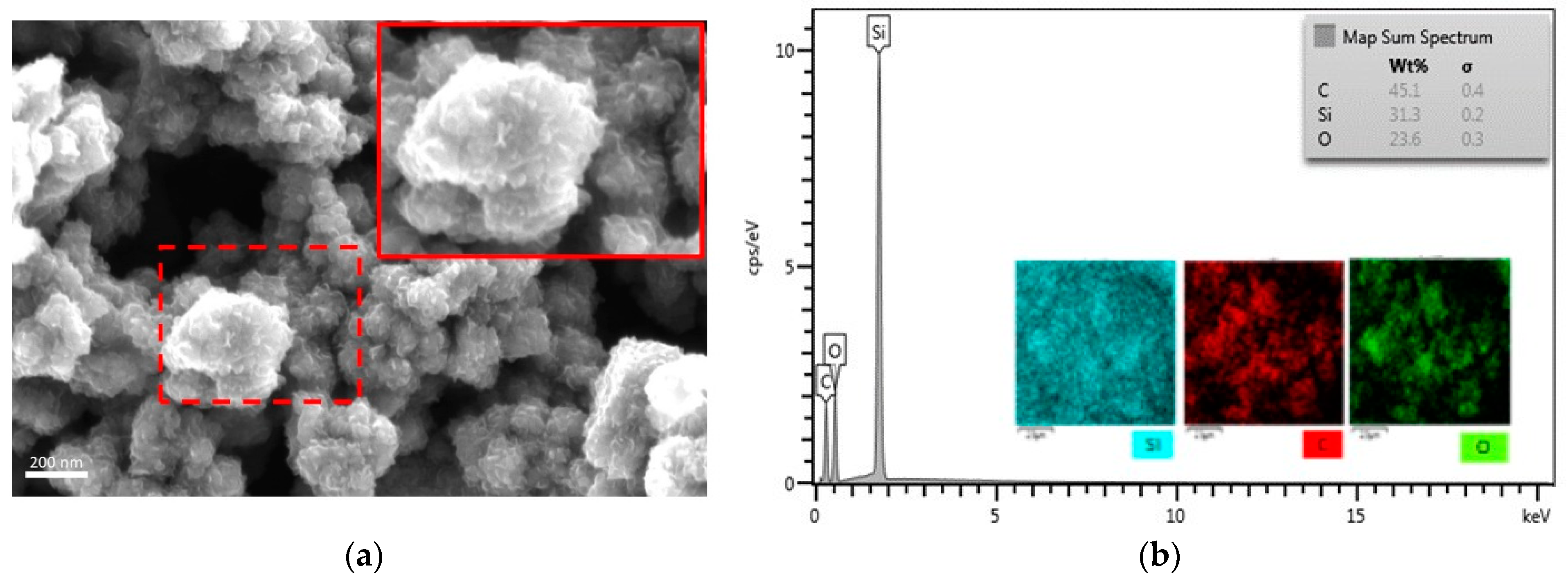
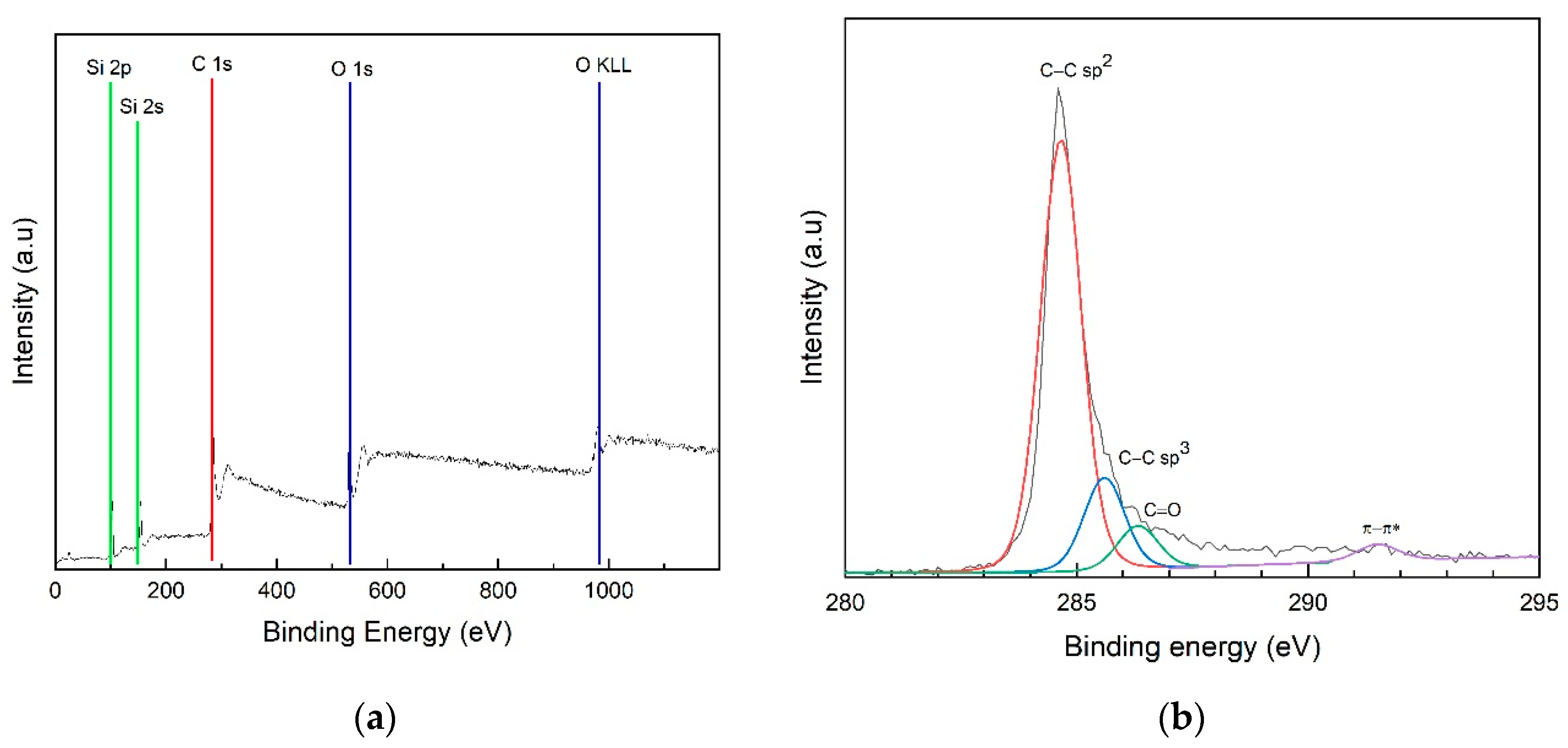
3.2.3. Chemical Composition

XPS measurements were performed to determine the chemical composition of the synthesized GBS at optimum conditions. Figure 6a shows the survey spectrum of SGB in which the presence of elements C 1s, Si 2p 2s, and O 1s can be observed. Figure 6b shows high-resolution XPS spectra for C sp2, sp3. Figure 6b shows the XPS analysis of graphene grown on the surface of SNPs. The presence of graphene was confirmed at the peak of 284.5 eV in the C–C characteristic group, indicating sp2 carbon bonding [26]. This XPS analysis aims to confirm that the SGB has graphene atomic bonds. Since graphene has high electrical conductivity, it is important to confirm that the SGB has an sp2 C–C bond.

3.2.4. Electrical Characterization of SGB

The Hall mobility (μHall) of the SGB reaches up to 550 cm2/Vs, with an average Hall effect coefficient (RHall) of 4.89 cm3/C and electrical conductivity of 75 S/cm. The positive value of the average RHall indicates that holes are the predominant charge carriers in the SGB. The RHall value is comparable to graphene grown on metal catalysts [25,40]. For comparison with the previous CVD method, our SGB exhibits a much higher average electrical conductivity compared to those of SGB grown via CH4 as the only gas during the growth process (∼40 S cm−1) [26] and graphene nanoballs grown with 20 min growth time (∼1 S cm−1) [27].

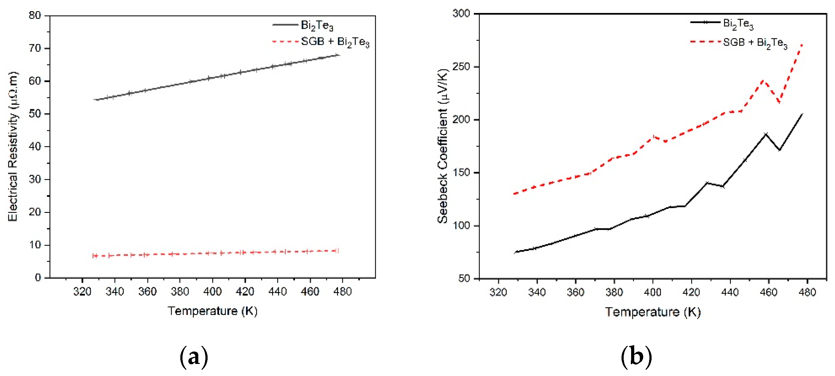
3.3. Material Evaluation for TE Application

In this work, the performance of SGB as nanofillers to improve the TE properties of TE generators was studied. TE generators’ efficiency is determined by the material’s performance, which is directly connected to the figure of merit, ZT = S 2 T / ρ κ , where S, ρ, κ, and T denote the Seebeck coefficient, electrical resistivity, thermal conductivity, and absolute temperature, respectively. Bi2Te3-based compounds have been widely commercialized as the best-performing room-temperature TE material.
The SGB were uniformly mixed in Bi2Te3 powder (0.5:99.5), and its effect on the TE properties of bulk nanocomposites was evaluated. Carbon burial sintering was used to prepare the bulk nanocomposites samples, as previously reported by [49]. Under the pressure of 40 MPa, the sample was cold-pressed in a stainless-steel die with a diameter of 12 mm and a thickness of 2–3 mm. Then, the sample was put in the alumina crucible surrounded by carbon powders and sintered at 474 K for 6 h.
The temperature dependence of the electrical resistivity for the samples is shown in Figure 7a. The electrical resistivity of pure Bi2Te3 (indicated by the black line) increases as the temperature increases from 320 K to 480 K, which indicates that the bulk materials exhibit a temperature dependence of the electrical resistivity described by metal-like or degenerated semiconductor behavior [50]. A significant drop in the electrical resistivity can be observed in the nanocomposite compared to the pure Bi2Te3 sample. This observation meets the statement made by Kaleem et al., who reported that graphene in SGB may account for the decrease in electrical resistance [51]. Figure 7b illustrates the Seebeck coefficients, S, for the samples. A significant increment in S is observed in the nanocomposite compared to the pure Bi2Te3 sample. It is more likely that the increase in the Seebeck coefficients, S, is due to the addition of SiO2 in SGB, which provides new barriers for charge carriers to overcome [52]. These early results suggest that this material has potential in optimizing TE properties for TE energy harvesters.

4. Conclusions

We successfully demonstrated an easy and fast method to directly grow graphene on SNP, called SGB, through a copper-vapor-assisted APCVD process. The detailed formation mechanisms for the SGB were proposed and investigated. Raman measurements support the existence of the sp2 carbon network. The morphology of the SGB is observed by FESEM as well as TEM. Although copper vapor is involved in the formation of SGB, the resulting SGB does not contain copper metal, as confirmed by FESEM-EDX. The investigation of the TE properties of the SGB as nanofillers in Bi2Te3 nanocomposites reveals significant improvements in the electrical resistivity and Seebeck coefficient as the temperature rises from 320 K to 480 K. We anticipate that our findings will spur additional research into using nanocomposites as a cost-effective strategy for significantly improving TE material performance at low operating temperatures.

Author Contributions

Conceptualization, N.Z., J.Y. and A.A.H.; methodology, N.Z., M.A.S.M.H., M.S.S., M.H.J. and D.; validation, M.A.S.M.H. and D.; formal analysis, N.Z., N.N.M.M. and A.A.M.R.; writing—original draft preparation, N.Z.; writing—review and editing, J.Y. and A.A.H.; supervision, J.Y. and A.A.H.; project administration, J.Y. and A.A.H.; funding acquisition, J.Y. and A.A.H. All authors have read and agreed to the published version of the manuscript.

Funding

This research was funded by the Dana Impak Perdana (DIP-2022-016) and Dana Pecutan Penerbitan (PP-IMEN-2203) research fund from the Ministry of Education, Malaysia.

Data Availability Statement

Data are contained within the article.

Acknowledgments

The authors would like to thank Dedi and Mohammad Dani Al Qori from Thermoelectric Lab, Badan Riset dan Inovasi Nasional (BRIN), Bandung, Indonesia for their contributions on thermoelectric material characterization.

Conflicts of Interest

The authors declare no conflict of interest.

References

  1. Handayani, M.; Nafi’ah, N.; Nugroho, A.; Rasyida, A.; Prasetyo, A.B.; Febriana, E.; Sulistiyono, E.; Firdiyono, F. The Development of Graphene/Silica Hybrid Composites: A Review for Their Applications and Challenges. Crystals 2021, 11, 1337. [Google Scholar] [CrossRef]
  2. Lee, J.H.; Kang, S.G.; Jang, H.S.; Moon, J.Y.; Whang, D. Graphene on Group-IV Elementary Semiconductors: The Direct Growth Approach and Its Applications. Adv. Mater. 2019, 31, 1803469. [Google Scholar] [CrossRef]
  3. Ding, L.P.; McLean, B.; Xu, Z.; Kong, X.; Hedman, D.; Qiu, L.; Page, A.J.; Ding, F. Why Carbon Nanotubes Grow. J. Am. Chem. Soc. 2022, 144, 5606–5613. [Google Scholar] [CrossRef]
  4. Mowlaei, R.; Lin, J.; Basquiroto de Souza, F.; Fouladi, A.; Habibnejad Korayem, A.; Shamsaei, E.; Duan, W. The Effects of Graphene Oxide-Silica Nanohybrids on the Workability, Hydration, and Mechanical Properties of Portland Cement Paste. Constr. Build. Mater. 2021, 266, 121016. [Google Scholar] [CrossRef]
  5. Selvarajan, R.S.; Rahim, R.A.; Majlis, B.Y.; Gopinath, S.C.B.; Hamzah, A.A. Ultrasensitive and Highly Selective Graphene-Based Field-Effect Transistor Biosensor for Anti-Diuretic Hormone Detection. Sensors 2020, 20, 2642. [Google Scholar] [CrossRef] [PubMed]
  6. Yang, N.; Chen, X.; Ren, T.; Zhang, P.; Yang, D. Carbon Nanotube Based Biosensors. Sens. Actuators B Chem. 2015, 207, 690–715. [Google Scholar] [CrossRef]
  7. Li, X.; Wang, R.; Wang, L.; Li, A.; Tang, X.; Choi, J.; Zhang, P.; Jin, M.L.; Joo, S.W. Scalable Fabrication of Carbon Materials Based Silicon Rubber for Highly Stretchable E-Textile Sensor. Nanotechnol. Rev. 2020, 9, 1183–1191. [Google Scholar] [CrossRef]
  8. Mohammad Haniff, M.A.S.; Muhammad Hafiz, S.; Wahid, K.A.A.; Endut, Z.; Wah Lee, H.; Bien, D.C.S.; Abdul Azid, I.; Abdullah, M.Z.; Ming Huang, N.; Abdul Rahman, S. Piezoresistive Effects in Controllable Defective HFTCVD Graphene-Based Flexible Pressure Sensor. Sci. Rep. 2015, 5, 14751. [Google Scholar] [CrossRef] [PubMed]
  9. Nurdin, M.; Agusu, L.; Putra, A.A.M.; Maulidiyah, M.; Arham, Z.; Wibowo, D.; Muzakkar, M.Z.; Umar, A.A. Synthesis and Electrochemical Performance of Graphene-TiO2-Carbon Paste Nanocomposites Electrode in Phenol Detection. J. Phys. Chem. Solids 2019, 131, 104–110. [Google Scholar] [CrossRef]
  10. Kothandam, G.; Singh, G.; Guan, X.; Lee, J.M.; Ramadass, K.; Joseph, S.; Benzigar, M.; Karakoti, A.; Yi, J.; Kumar, P.; et al. Recent Advances in Carbon-Based Electrodes for Energy Storage and Conversion. Adv. Sci. 2023, 10, 2301045. [Google Scholar] [CrossRef]
  11. Ye, Z.; Wu, P.; Wang, H.; Jiang, S.; Huang, M.; Lei, D.; Wu, F. Multimode Tunable Terahertz Absorber Based on a Quarter Graphene Disk Structure. Results Phys. 2023, 48, 106420. [Google Scholar] [CrossRef]
  12. Kuzhir, P.; Celzard, A.; Chen, X. Microwave Absorption by Carbon-Based Materials and Structures. J. Appl. Phys. 2022, 131, 200401. [Google Scholar] [CrossRef]
  13. Ahmadipour, M.; Hamzah, A.A.; Pang, A.L.; Thi Le, A.; Chiam, S.L.; Ahmad, Z.A.; Rajitha, B.; Pung, S.Y. Photodegradation of Rhodamine B-Dye Pollutant Using CaCu3Ti4O12-Multiwall Carbon Nanotube Nanocomposites. J. Environ. Chem. Eng. 2021, 9, 105185. [Google Scholar] [CrossRef]
  14. Li, X.; Yu, J.; Wageh, S.; Al-Ghamdi, A.A.; Xie, J. Graphene in Photocatalysis: A Review. Small 2016, 12, 6640–6696. [Google Scholar] [CrossRef]
  15. Hatta, F.F.; Mohammad Haniff, M.A.S.; Mohamed, M.A. A Review on Applications of Graphene in Triboelectric Nanogenerators. Int. J. Energy Res. 2021, 46, 544–576. [Google Scholar] [CrossRef]
  16. Tao, T.; Li, G.; He, Y.; Yang, X. 3-D Magnetic Graphene Balls as Sorbents for Cleaning Oil Spills. Nanomater. Nanotechnol. 2019, 9, 184798041985737. [Google Scholar] [CrossRef]
  17. Solati, E.; Savadkoohi, M.; Dorranian, D. Nonlinear Optical Response of Graphene/Silicon Nanocomposites. Opt. Quantum Electron. 2018, 50, 268. [Google Scholar] [CrossRef]
  18. Ye, W.; Zhang, L.; Li, C. Facile Fabrication of Silica-Polymer-Graphene Collaborative Nanostructure-Based Hybrid Materials with High Conductivity and Robust Mechanical Performance. RSC Adv. 2015, 5, 25450–25456. [Google Scholar] [CrossRef]
  19. Ho, S.; Kang, Y.C. Fe3O4-Decorated Hollow Graphene Balls Prepared by Spray Pyrolysis Process for Ultrafast and Long Cycle-Life Lithium Ion Batteries. Carbon N. Y. 2014, 79, 58–66. [Google Scholar] [CrossRef]
  20. Chen, D.; Yi, R.; Chen, S.; Xu, T.; Gordin, M.L.; Wang, D. Facile Synthesis of Graphene—Silicon Nanocomposites with an Advanced Binder for High-Performance Lithium-Ion Battery Anodes. Solid State Ionics 2014, 254, 65–71. [Google Scholar] [CrossRef]
  21. Chen, J.; Wen, Y.; Guo, Y.; Wu, B.; Huang, L.; Xue, Y.; Geng, D.; Wang, D.; Yu, G.; Liu, Y. Oxygen-Aided Synthesis of Polycrystalline Graphene on Silicon Dioxide Substrates. J. Am. Chem. Soc. 2011, 133, 17548–17551. [Google Scholar] [CrossRef] [PubMed]
  22. Saeed, M.; Alshammari, Y.; Majeed, S.A.; Al-Nasrallah, E. Chemical Vapour Deposition of Graphene—Synthesis, Characterisation, and Applications: A Review. Molecules 2020, 25, 3856. [Google Scholar] [CrossRef] [PubMed]
  23. Jafari, A.; Ghoranneviss, M.; Hantehzadeh, M.R. Morphology Control of Graphene by LPCVD. J. Fusion Energy 2015, 34, 532–539. [Google Scholar] [CrossRef]
  24. Madito, M.J.; Matshoba, K.S.; Mongwaketsi, N.; Mtshali, C.B.; Fabiane, M.; Manyala, N. Nickel-Copper Graphene Foam Prepared by Atmospheric Pressure Chemical Vapour Deposition for Supercapacitor Applications. Surf. Coat. Technol. 2020, 383, 125230. [Google Scholar] [CrossRef]
  25. Yen, W.C.; Chen, Y.Z.; Yeh, C.H.; He, J.H.; Chiu, P.W.; Chueh, Y.L. Direct Growth of Self-Crystallized Graphene and Graphite Nanoballs with Ni Vapor-Assisted Growth: From Controllable Growth to Material Characterization. Sci. Rep. 2014, 4, 4739. [Google Scholar] [CrossRef]
  26. Son, I.H.; Park, J.H.; Park, S.; Park, K.; Han, S.; Shin, J.; Doo, S.G.; Hwang, Y.; Chang, H.; Choi, J.W. Graphene Balls for Lithium Rechargeable Batteries with Fast Charging and High Volumetric Energy Densities. Nat. Commun. 2017, 8, 1561. [Google Scholar] [CrossRef]
  27. Zhao, B.; Sun, T.; Zhou, X.; Liu, X.; Li, X.; Zhou, K.; Dong, L.; Wei, D. Three-Dimensional Graphene Composite Containing Graphene-SiO2 Nanoballs and Its Potential Application in Stress Sensors. Nanomaterials 2019, 9, 438. [Google Scholar] [CrossRef]
  28. Zainal Ariffin, N.H.; Mohammad Haniff, M.A.S.; Syono, M.I.; Ambri Mohamed, M.; Hamzah, A.A.; Hashim, A.M. Low-Temperature Nitrogen Doping of Nanocrystalline Graphene Films with Tunable Pyridinic-N and Pyrrolic-N by Cold-Wall Plasma-Assisted Chemical Vapor Deposition. ACS Omega 2021, 6, 23710–23722. [Google Scholar] [CrossRef]
  29. Fauzi, F.B.; Ismail, E.; Syed Abu Bakar, S.N.; Ismail, A.F.; Mohamed, M.A.; Md Din, M.F.; Illias, S.; Ani, M.H. The Role of Gas-Phase Dynamics in Interfacial Phenomena during Few-Layer Graphene Growth through Atmospheric Pressure Chemical Vapour Deposition. Phys. Chem. Chem. Phys. 2020, 22, 3481–3489. [Google Scholar] [CrossRef]
  30. Wang, S.; Hibino, H.; Suzuki, S.; Yamamoto, H. Atmospheric Pressure Chemical Vapor Deposition Growth of Millimeter-Scale Single-Crystalline Graphene on the Copper Surface with a Native Oxide Layer. Chem. Mater. 2016, 28, 4893–4900. [Google Scholar] [CrossRef]
  31. Mohamad, N.R.; Wee, M.F.M.R.; Mohamed, M.A.; Hamzah, A.A.; Menon, P.S. Multi-Response Optimization of Chromium/Gold-Based Nanofilm Kretschmann-Based Surface Plasmon Resonance Glucose Sensor Using Finite-Difference Time-Domain and Taguchi Method. Nanomater. Nanotechnol. 2020, 10, 1–15. [Google Scholar] [CrossRef]
  32. Freddi, A.; Salmon, M. Introduction to the Taguchi Method. In Design Principles and Methodologies; Springer Tracts in Mechanical Engineering; Springer: Cham, Switzerland, 2019; pp. 159–180. ISBN 9783319953427. [Google Scholar]
  33. Papon, R.; Pierlot, C.; Sharma, S.; Shinde, S.M.; Kalita, G.; Tanemura, M. Optimization of CVD Parameters for Graphene Synthesis through Design of Experiments. Phys. Status Solidi Basic Res. 2017, 254, 1600629. [Google Scholar] [CrossRef]
  34. Tahir, N.A.M.; Bin Abdollah, M.F.; Tamaldin, N.; Zin, M.R.B.M.; Amiruddin, H. Optimisation of Graphene Grown from Solid Waste Using CVD Method. Int. J. Adv. Manuf. Technol. 2020, 106, 211–218. [Google Scholar] [CrossRef]
  35. Nolas, G.S.; Sharp, J.; Goldsmid, J. Thermoelectrics: Basic principles and new materials developments. In Science and Technology; Springer Science & Business Media: Berlin/Heidelberg, Germany, 2013; Volume 45, p. 228. ISBN 9781461257080. [Google Scholar]
  36. Ma, M.; Li, H.; Xiong, Y.; Dong, F. Rational Design, Synthesis, and Application of Silica/Graphene-Based Nanocomposite: A Review. Mater. Des. 2021, 198, 109367. [Google Scholar] [CrossRef]
  37. Teng, P.Y.; Lu, C.C.; Akiyama-Hasegawa, K.; Lin, Y.C.; Yeh, C.H.; Suenaga, K.; Chiu, P.W. Remote Catalyzation for Direct Formation of Graphene Layers on Oxides. Nano Lett. 2012, 12, 1379–1384. [Google Scholar] [CrossRef] [PubMed]
  38. Kim, H.; Song, I.; Park, C.; Son, M.; Hong, M.; Kim, Y.; Kim, J.S.; Shin, H.-J.; Baik, J.; Choi, H.C. Copper-Vapor-Assisted Chemical Vapor Deposition for High-Quality and Metal-Free Single-Layer Graphene on Amorphous SiO2 Substrate. ACS Nano 2013, 7, 6575–6582. [Google Scholar] [CrossRef]
  39. Zhang, W.; Zhang, L.; Zhang, H.; Song, L.; Ye, Q.; Cai, J. Synthesize Monolayer Graphene on SiO2/Si Substrate with Copper-Vapor-Assisted CVD Method. Mater. Res. Express 2018, 5, 125601. [Google Scholar] [CrossRef]
  40. Zhou, L.; Wei, S.; Ge, C.; Zhao, C.; Guo, B.; Zhang, J.; Zhao, J. Ultrafast Growth of Uniform Multi-Layer Graphene Films Directly on Silicon Dioxide Substrates. Nanomaterials 2019, 9, 964. [Google Scholar] [CrossRef]
  41. Li, Y.; Li, Z.; Li, Q.; Tian, M.; Li, C.; Sun, L.; Wang, J.; Zhao, X.; Xu, S.; Yu, F. Direct Synthesis of Graphene Dendrites on SiO2/Si Substrates by Chemical Vapor Deposition. Nanoscale Res. Lett. 2020, 15, 1–10. [Google Scholar] [CrossRef]
  42. Ren, S.; Rong, P.; Yu, Q. Preparations, Properties and Applications of Graphene in Functional Devices: A Concise Review. Ceram. Int. 2018, 44, 11940–11955. [Google Scholar] [CrossRef]
  43. Ferrari, A.C. Raman Spectroscopy of Graphene and Graphite: Disorder, Electron–Phonon Coupling, Doping and Nonadiabatic Effects. Solid State Commun. 2007, 143, 47–57. [Google Scholar] [CrossRef]
  44. Rushforth, R.J. Review of Design Experiments Using the Taguchi Approach: 16 Steps to Product and Process Improvement; American Society for Testing and Materials: West Conshohocken, PA, USA, 2001; Volume 29, ISBN 978-0-471-36101-5. [Google Scholar]
  45. Childres, I.; Jauregui, L.A.; Park, W.; Caoa, H.; Chena, Y.P. Raman Spectroscopy of Graphene and Related Materials. New Dev. Phot. Mater. Res. 2013, 1, 403–418. [Google Scholar]
  46. Malard, L.M.; Pimenta, M.A.; Dresselhaus, G.; Dresselhaus, M.S. Raman Spectroscopy in Graphene. Phys. Rep. 2009, 473, 51–87. [Google Scholar] [CrossRef]
  47. Vicarelli, L.; Heerema, S.J.; Dekker, C.; Zandbergen, H.W. Controlling Defects in Graphene for Optimizing the Electrical Properties of Graphene Nanodevices. ACS Nano 2015, 9, 3428–3435. [Google Scholar] [CrossRef] [PubMed]
  48. Ma, Y.; Jang, H.; Kim, S.J.; Pang, C.; Chae, H. Copper-Assisted Direct Growth of Vertical Graphene Nanosheets on Glass Substrates by Low-Temperature Plasma-Enhanced Chemical Vapour Deposition Process. Nanoscale Res. Lett. 2015, 10, 308. [Google Scholar] [CrossRef]
  49. Kristiantoro, T.; Dedi; Fauzia, V. Synthesis and Characterization of Bi2Te3 Thermoelectric Material Using the Cold Pressing and Sintering Method. IOP Conf. Ser. Mater. Sci. Eng. 2019, 553, 012033. [Google Scholar] [CrossRef]
  50. Zhu, Y.K.; Wu, P.; Guo, J.; Zhou, Y.; Chong, X.; Ge, Z.H.; Feng, J. Achieving a Fine Balance in Mechanical Properties and Thermoelectric Performance in Commercial Bi2Te3 Materials. Ceram. Int. 2020, 46, 14994–15002. [Google Scholar] [CrossRef]
  51. Ahmad, K.; Wan, C.; Zong, P.A. Thermoelectric Properties of BiSbTe/Graphene Nanocomposites. J. Mater. Sci. Mater. Electron. 2019, 30, 11923–11930. [Google Scholar] [CrossRef]
  52. Nozariasbmarz, A.; Krasinski, J.S.; Vashaee, D. N-Type Bismuth Telluride Nanocomposite Materials Optimization for Thermoelectric Generators in Wearable Applications. Materials 2019, 12, 1529. [Google Scholar] [CrossRef] [PubMed]
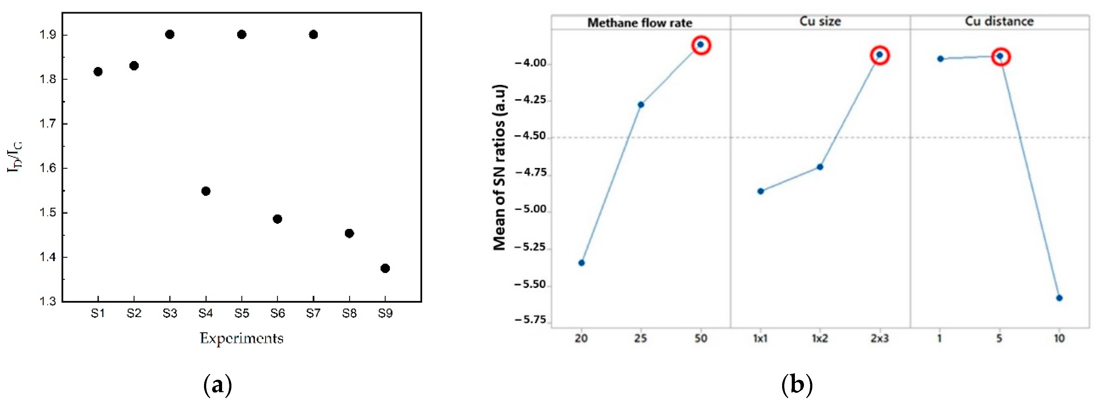
Figure 1. (a) Distance-dependent growth of SGB. Arrow shows the distance between copper foil and SNP. (b) Experimental protocol of SGB synthesis using APCVD. Arrow shows the duration of the gasses exposed during graphene growth.
Nanomaterials 14 00618 g001
Figure 2. (a) ID/IG derived from Raman spectra. (b) Main effects plot for SN ratios of SGB growth. The red circle shows the maximum value of Mean of SN ratios, therefore the value is the optimum parameter for SGB growth process.
Nanomaterials 14 00618 g002
Figure 3. Raman spectra: (a) SGB at optimum condition; (b) comparison between SGB growth with copper and nickel as catalysts; (c) comparison between SGB growth with and without copper as catalysts.
Nanomaterials 14 00618 g003
Figure 4. SGB at optimum condition: (a) FESEM image, the red lined shows zoomed specified spot shown by the small box with red dash line; (b) EDX spectra.
Nanomaterials 14 00618 g004
Figure 5. TEM micrographs of SNP and SGB at the optimum condition: (a) initial SNP; (b) SNP after coated with graphene; (c) SGB 3D sheet morphology; (d) the selected area of electron diffraction (SAED) pattern, obtained at 120 kV.
Nanomaterials 14 00618 g005
Figure 6. X-ray photoelectron spectroscopy (XPS) spectrum of SGB at the optimum condition: (a) the survey spectrum; (b) curve fit of C1s peak.
Nanomaterials 14 00618 g006
Figure 7. Temperature dependence of (a) electrical resistivity, ρ, and (b) Seebeck coefficient, S, of SGB/Bi2Te3 nanocomposites and pure Bi2Te3.
Nanomaterials 14 00618 g007
Table 2. Taguchi-designed trial experiment for SGB APCVD.
ExperimentsFactors
Methane Flow Rate, ΦCH4 (sccm)Copper Foil Size, CS
(cm)
Copper Distance, CD
(cm)
S1201 × 11
S2201 × 25
S3202 × 310
S4251 × 15
S5251 × 210
S6252 × 31
S7501 × 110
S8501 × 21
S9502 × 35
Disclaimer/Publisher’s Note: The statements, opinions and data contained in all publications are solely those of the individual author(s) and contributor(s) and not of MDPI and/or the editor(s). MDPI and/or the editor(s) disclaim responsibility for any injury to people or property resulting from any ideas, methods, instructions or products referred to in the content.

