Abstract
InAs quantum wells (QWs) are promising material systems due to their small effective mass, narrow bandgap, strong spin–orbit coupling, large g-factor, and transparent interface to superconductors. Therefore, they are promising candidates for the implementation of topological superconducting states. Despite this potential, the growth of InAs QWs with high crystal quality and well-controlled morphology remains challenging. Adding an overshoot layer at the end of the metamorphic buffer layer, i.e., a layer with a slightly larger lattice constant than the active region of the device, helps to overcome the residual strain and provides optimally relaxed lattice parameters for the QW. In this work, we systematically investigated the influence of overshoot layer thickness on the morphological, structural, strain, and transport properties of undoped InAs QWs on GaAs(100) substrates. Transmission electron microscopy reveals that the metamorphic buffer layer, which includes the overshoot layer, provides a misfit dislocation-free InAs QW active region. Moreover, the residual strain in the active region is compressive in the sample with a 200 nm-thick overshoot layer but tensile in samples with an overshoot layer thicker than 200 nm, and it saturates to a constant value for overshoot layer thicknesses above 350 nm. We found that electron mobility does not depend on the crystallographic directions. A maximum electron mobility of 6.07 × 105 cm2/Vs at 2.6 K with a carrier concentration of 2.31 × 1011 cm−2 in the sample with a 400 nm-thick overshoot layer has been obtained.
1. Introduction
InAs and high In-content InGaAs/InAlAs quantum wells (QWs) are attractive material systems due to their small effective mass, narrow bandgap, strong spin–orbit coupling, large g-factor, and transmissive interface to superconductors [1,2,3,4,5]. Recent studies have shown that InAs is an excellent candidate for high-speed electronic devices, optoelectronics, spintronics, quantum computing, and topological superconducting circuits [4,5,6,7,8,9,10,11,12]. Furthermore, InAs-based two-dimensional electron gases (2DEGs) with an in situ deposited Al epitaxial layer led to the observation of conductance quantization in quantum point contacts [4,11], to the realization of Josephson junctions with tunable supercurrent [11], and the observation of Andreev bound states that may host Majorana zero modes [4,12].
One of the fundamental issues of scalability with the growth of high-quality and high-mobility InAs and high In-content InGaAs/InAlAs QWs is the large lattice mismatch with commonly available substrates. The only lattice-matched substrates for growing InAs and high In-content InGaAs/InAlAs QWs are InAs and GaSb. Since InAs substrates are conductive, they are not suitable for electronic applications. On the other hand, GaSb substrates are very expensive, and tellurium rather than silicon must be used to dope the AlGaSb barriers [13,14]. To overcome these issues, researchers have implemented step-graded metamorphic buffer layers (MBLs) of InGaAs or InAlAs on GaAs and InP substrates [3,4,5,15,16,17,18,19,20]. Step-graded MBLs allow the achievement of virtually strain-free and dislocation-free QWs by producing misfit dislocations at compositional steps in the metamorphic buffer layer far from the active region of the structure. Recently, Benali et al. [16] and Hatke et al. [4] reported the highest-ever mobility of 7 × 105 cm2/Vs and 1 × 106 cm2/Vs at 4.2 K for InAs/InGaAs QWs on GaAs(001) and InP(100) substrates, respectively. For quantum computing and superconducting applications, GaAs substrates are more attractive due to the high resistivity shown and, therefore, this work has been devoted to the study of MBLs on GaAs substrates.
High electron mobility is an important requisite to investigate the fundamental properties of materials. Therefore, it is crucial to determine the factors limiting electron mobility. A lot of work has already been performed, and in this process, the properties of these materials [3,4,5,15,16,17,18,19,20] have been improved. Ionized impurity and alloy disorder scattering are the main scattering mechanisms affecting mobility at low temperatures [3,4,15,21]. Recently, Hatke [4] et al. and Shabani et al. [22] experimentally confirmed that unintentional impurities limit the mobility of undoped InAs/InGaAs QWs. Another interesting result is that InAs/InGaAs and InGaAs QWs grown on standard GaAs(100) wafers are reported to show an anisotropy in mobility [3,5,20,21,23]. The mobility was found to be higher along the direction compared to the [110] direction [3,20,21,23]. This effect was attributed to several reasons, such as interface roughness, indium concentration modulation, asymmetric strain relaxation, anisotropic ordering effects, and anisotropic growth of dislocations [3,5,20,21,23,24].
In this work, we investigate undoped InAs/In0.81Ga0.19As QWs grown using solid source Molecular Beam Epitaxy (MBE) on semi-insulating GaAs(100) substrates. We systematically investigated their morphological, structural, strain, and transport properties. First, we studied the evolution of surface morphology by performing atomic force microscopy (AFM). Then, a study of the structural quality was performed in cross-section using transmission electron microscopy (TEM). The residual strain was determined using X-ray diffraction (XRD) rocking curves and reciprocal space maps (RSMs). To derive the sheet carrier density and mobility of samples at 4.2 K, we first performed Hall measurements in the van der Pauw configuration. Then, the electron mobility in and [110] directions was determined via Hall bars (HBs) at 2.6 K. This study allowed us to demonstrate that optimizing the residual strain of the buffer layer provides an efficient way to achieve excellent electrical properties of InAs 2DEGs. Moreover, within error bars, the electron mobility is independent of crystallographic directions due to the strong confinement of the wave function of the carriers inside the binary InAs QW.
2. Experimental Details
The QWs studied in this paper were grown on semi-insulating GaAs(100) substrates via solid source Molecular Beam Epitaxy (MBE) in a Riber compact 21 DZ system (Riber, Paris, France). A schematic of our heterostructure adapted from Refs. [15,16] is shown in Figure 1. The sequence of the layer structure in all samples, starting from the substrate, is as follows: a 200 nm GaAs layer, a 100 nm GaAs/AlGaAs superlattice (SL), a 200 nm GaAs layer, a 1250 nm step-graded InxAl1−xAs metamorphic buffer layer with x increasing from 0.15 to 0.81, an overshoot layer with In concentration x = 0.84, and an active region with In concentration x = 0.81. The buffer layer consists of two regions with different misfit gradients df/dt. The first region is composed of twelve 50 nm steps with x ramping from 0.15 to 0.58, corresponding to a misfit gradient of 5.1% μm−1. The second region is composed of twelve 50 nm steps with x ramping from 0.58 to 0.81, corresponding to a misfit gradient around 3.1% μm−1. The flux of Al was kept constant during the buffer layer growth, while the In cell temperature was increased at each step without growth interruptions. The active part of the sample from the buffer layer to the free surface is composed of a 50 nm In0.81Al0.19As barrier, a 9 nm In0.81Ga0.19As layer, a 7 nm InAs QW, a 9 nm In0.81Ga0.19As layer, a 117 nm In0.81Al0.19As barrier, and a 3 nm In0.81Ga0.19As capping layer. The buffer layer and the active part were grown at optimized substrate temperatures of (320 ± 5) °C and (480 ± 5) °C, respectively. The arsenic flux was adjusted during the growth to keep a group V/III beam flux ratio of 8 throughout the growth. A growth rate of about 1.3 μm/h was used for the active region. Although nominally undoped, electronic charge in the quantum well is due to a deep-level donor state in the InAlAs barrier band gap, whose energy lies within the InGaAs/InAlAs conduction band discontinuity [25]. A series of samples with different overshoot layer thicknesses was grown to study the effect of strain relaxation on the transport properties of the InAs QWs. The samples presented in this study have different overshoot layer thicknesses (tOS) of 200 nm, 250 nm, 300 nm, 350 nm, and 400 nm and are labeled as A, B, C, D, and E, respectively.
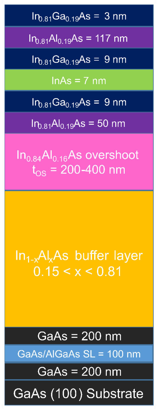
Figure 1.
A schematic of the layer structure (not to scale).
The surface morphology of the grown samples was studied using a Bruker Dimension Icon atomic force microscope (AFM) (Bruker, Köln, Germany). The scans were performed in the air using the ScanAsyst operative mode (NanoScope, 9.1), which is a non-resonance tapping mode. The tip is made of silicon nitride and has a radius of < 10 nm and a height of 2.5–8 µm. To investigate different regions of the sample, we performed scans of 10 × 10 μm2, 20 × 20 μm2, and 50 × 50 μm2 areas.
Samples for TEM observations were prepared in both plan-view and cross-section using the standard mechano-chemical thinning procedure. The useful thickness for electron transparency was obtained with final thinning in the GATAN 691 Precision Ion Polishing System (PIPS) (Pleasanton, CA, USA). The samples were observed in both conventional TEM and High-Angle Annular Dark-Field scanning TEM (HAADF-STEM) imaging modes in an analytical JEOL 2200FS UHR (Tokyo, Japan) field emission microscope, using standard rules for dislocation contrast optimization.
X-ray diffraction (XRD) measurements were performed to investigate the In concentration and residual strain in the QWs using a QC3 Bruker (Bruker, Migdal Ha’Emek, Israel) high-resolution diffractometer. The X-ray tube consists of a tungsten filament and a copper anode, operating at a voltage of 40 kV and a current of 40 mA. The X-ray optics consist of a parabolic graded multilayer mirror and a channel-cut collimator with a 2-bounce Ge(004) crystal. The parabolic mirror parallelizes the beam with a divergence of 0.1°, while the 2-bounce Ge(004) monochromator selects the Cu Kα1 wavelength (1.54059 Å). Symmetric (004) and asymmetric (115) ω-2θ scans were performed to calculate the out-of-plane and in-plane lattice constants of lattice-mismatched epilayers grown on top of the GaAs(100) substrate. Reciprocal space maps (RSMs) of sample E were acquired with a Philips (Amsterdam, Netherlands) X-Pert high-resolution XRD equipped with a Bartels (Hamburg, Germany) four-crystal Ge(220) monochromator, using Cu Kα1 radiation with a 12 arcsec angular divergence. We have measured reciprocal lattice maps of (004) and (224) diffraction along [110] and scattering planes by setting the azimuthal angle φ to angles 0°/180° and 90°/270°.
Transport measurements of all samples were performed at 4.2 K on ~4 × 4 mm2 samples in van der Pauw geometry. A Hall-bar (HB) geometry was used to determine if any anisotropic mobility was present in sample E (the sample with the highest electron mobility) at 2.3 K. HBs of dimensions (L W) = 550 100 µm2 were fabricated along the and [110] directions via optical lithography and wet etching. Here, L is the length, and W is the width of the HB. Electrical contact to the 2DEG is guaranteed by alloyed Ni/Ge/Au Ohmic contacts. The distance between the longitudinal contacts was 250 µm.
3. Results and Discussion
The surface morphology of all samples with different overshoot layer thicknesses was investigated using AFM. The AFM micrographs were acquired on the free surface of the samples (the capping layer of the samples), which reflects the morphology of the buried InxAl1−xAs/InxGa1−xAs interfaces. As an example, we show AFM micrographs of samples A (200 nm-thick overshoot layer) and E (400 nm-thick overshoot layer) and corresponding line scans shown in Figure 2. All samples show a cross-hatched pattern oriented along the two orthogonal directions and [110]. The cross-hatched patterns are periodic undulations of surface morphology typical of lattice-mismatched heteroepitaxy. Such striations derive from an inhomogeneous strain relaxation process caused by interfacial misfit dislocations buried in the buffer layer [5,15,18,26]. For all samples, we find a similar two-dimensional root mean square (RMS) roughness of the sample surface, with a value of (3.2 ± 1) nm. The RMS value given above is the average from three images of size 20 × 20 μm2 acquired from different regions of each sample. Furthermore, we obtained the one-dimensional RMS roughness of the samples along the and [110] directions by analyzing line scans of 10 µm. The RMS roughness of sample A along the and [110] directions is (1.90 ± 0.3) nm and (2.50 ± 0.6) nm, respectively, while for sample E, it is (1.86 ± 0.3) nm and (1.92 ± 0.6) nm, respectively. Thus, no significant difference between the two orthogonal crystallographic directions was observed. On the other hand, the period of the surface oscillations does depend on the crystallographic direction. It is shorter in the [110] direction and longer in the direction. The average period of undulations for samples A and E in the [110] direction is (540 ± 140) nm and (505 ± 70) nm, respectively. In the direction, the average period of undulations for samples A and E is (1340 ± 225) nm and (1470 ± 250) nm, respectively. These AFM findings agree well with prior studies [15,16,18].
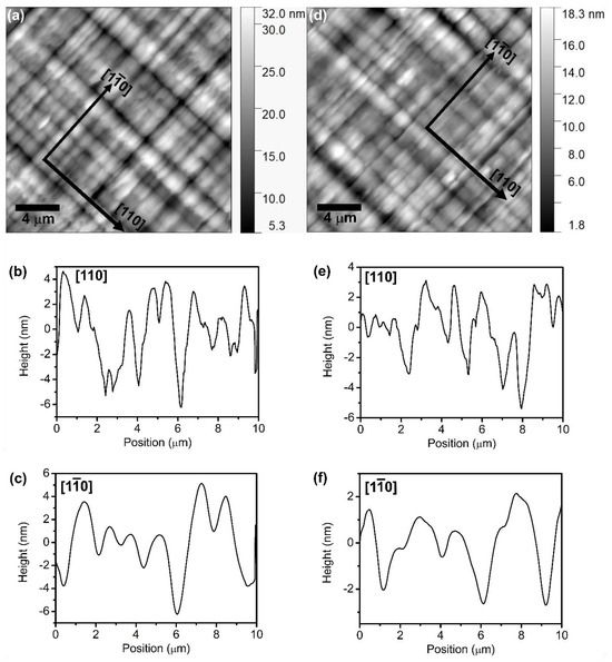
Figure 2.
(a) 20 × 20 μm2 AFM image showing the surface morphology of sample A. (b) Height profile along the [110] direction of sample A. (c) Height profile along the direction of sample A. (d) 20 × 20 μm2 AFM image showing the surface morphology of sample E. (e) Height profile along the [110] direction of sample E. (f) Height profile along the direction of sample E.
The distribution of dislocations across the metamorphic buffer layer was studied using TEM on sample C (300 nm overshoot layer thickness) and sample E (400 nm overshoot layer thickness), both in plan view and cross-section. The study of the planar sections was carried out in areas of tens of square microns throughout the electron-transparent zone (the maximum thickness for reliable observation is equal to approximately 500 nm from the sample surface). No misfit dislocations were observed in both samples. However, occasional threading dislocations emerging at the surface were observed, as shown in Figure 3a. Their density was estimated to be approximately 107 cm−2, without notable differences between the two samples. The poor statistics intrinsic to the technique make this estimate less precise. Figure 3a,b show cross-sectional dark field Scanning TEM images of samples C and E, respectively, taken along a <110> axis. TEM images were captured in areas up to 10 µm in length. The different regions of the layer structure are marked in the images. Two regimes are clearly observed in both samples: a region close to the substrate with a high density of misfit dislocations and a region near the surface where no misfit dislocations are observed, consistent with the plan-view investigations. All misfit dislocations are confined within the graded metamorphic buffer layer. The distance measured from the surface to the last misfit dislocation layer for samples C and E is (505 ± 10) nm and (625 ± 5) nm, respectively. The difference between the two samples is due to their different overshoot layer thickness, which, thus, does not contain any misfit dislocations. These results confirm that, by carefully choosing the design of the metamorphic buffer layer, the active region can be grown free from misfit dislocations.
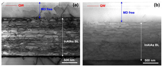
Figure 3.
Cross-sectional STEM-HAADF images of (a) sample C; and (b) sample E.
Figure 4a shows a high-resolution STEM-HAADF image of the In0.81Ga0.19As/InAs/In0.81Ga0.19As layers obtained from sample E. The InAs QW is indicated in the image. The InAs layer appears brighter and more clearly visible than the In0.81Ga0.19As layers due to its higher average atomic number with respect to the barriers. This allowed us to determine the thickness of the InAs QW as (7.5 ± 0.5) nm, which is in good agreement with the nominal thickness. The energy dispersive X-ray spectroscopy (EDS) line scan analysis using the Kα1 emission of Ga and the Lα1 emission of In along the red line marked in panel (a) confirmed that Ga is present only in the two layers bordering the InAs QW (Figure 4b). The broadening of the signal is due to the size of the characteristic X-ray generation volume, which is larger than the InAs QW.
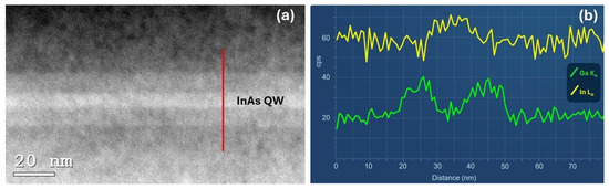
Figure 4.
(a) STEM-HAADF image of the In0.81Ga0.19As/InAs/In0.81Ga0.19As layers of sample E. (b) EDS line scan obtained along the red line in panel (a).
To measure the residual strain in the samples, we performed XRD measurements in triple-axis configuration along 0° and 180° azimuth in the vicinity of the (004) reflection. Figure 5a compares the ω-2θ scans of the series of samples with increasing overshoot layer thickness, measured under 0° azimuth. All spectra display three main peaks: the substrate peak, the active region (AR) peak, and the overshoot (OS) layer peak. The peak with the highest intensity is the substrate peak. The broad features in the range from -7000 arcsec to -1500 arcsec originate from the metamorphic buffer layer. Around -5000 arcsec, there is a small peak corresponding to an indium content of 0.58, which is associated with the accumulation of an InxAl1−xAs layer with x = 0.58, at which the slope of the indium profile in the structure changes. The similar position of this peak for all samples indicates that the buffer layer profiles are the same. Therefore, the changes in the strain relaxation of the active region can be uniquely associated with the differences in the thickness of the overshoot layers.
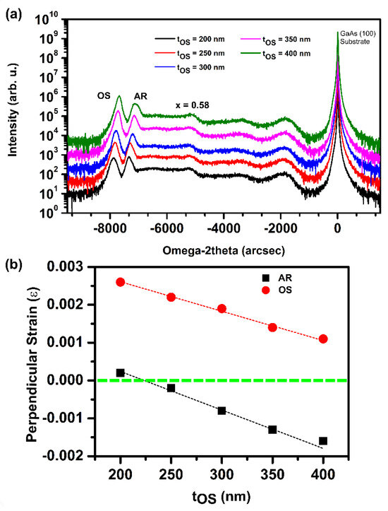
Figure 5.
(a) (004) ω-2θ scans obtained along the 0° azimuth from a series of InAs/In0.81Ga0.19As QW samples with different overshoot thicknesses tOS. (b) Residual perpendicular strain in the active region (x = 0.81, black) and in the overshoot layer (x = 0.84, red).
We observed that both the AR and the OS peaks shift to the right with increasing tOS due to different strain relaxation in these layers. We calculated the residual perpendicular strain in the active region and in the overshoot layer, assuming the nominal composition and using Vegard’s law. The residual strain of the samples is plotted in Figure 5b as a function of overshoot thickness tOS. The overshoot layers are compressively strained for all tOS, but with increasing tOS, the strain decreases. Instead, the strain in the active region switches from compressive to tensile and tends to saturate above 350 nm, where the overshoot layer is nearly relaxed. In summary, by varying the thickness of the overshoot layer, it is possible to tune the strain in the active region to achieve a virtual substrate that is lattice-matched to the active region.
Sample E is further investigated by measuring RSMs near symmetric (004) and asymmetric (224) nodes, with the diffracting plane inclined 35.26° with respect to the (001) nominal surface. The residual strain was measured in both and [110] directions by setting the azimuthal angle φ to angles 0°/180° and 90°/270°, respectively, corresponding to (2−24), (224), (−224), and (−2−24) diffracting planes. Figure 6 shows symmetric (004) RSMs of sample E with scattering planes parallel to and [110] directions. All maps show three different intense spots corresponding to the substrate, the AR, and the OS. The AR and OS peaks appear shifted with respect to the position of the substrate peak due to (a) the presence of small unintentional miscuts (α(1−10) = 0.32°; α (110) = 0.13°) of the crystal surface with respect to the (001) nominal orientation, and (b) due to lattice tilts of OS and AR with respect to the substrate lattice (α (1−10) = 0.10°; α (110) = 0.27°), due to unbalanced Burgers vector components of misfit dislocations perpendicular to the (001) surface [27]. Since such dislocations are buried in the buffer layer, the tilt is the same for both OS and AR. We also note larger mosaic spreads of OS and AR peaks in maps parallel to the [110] direction. This is an indication of a higher dislocation density, and hence a higher strain release, along the [110] direction. Consistent with this [28,29], the lattice tilt is also larger along this direction.
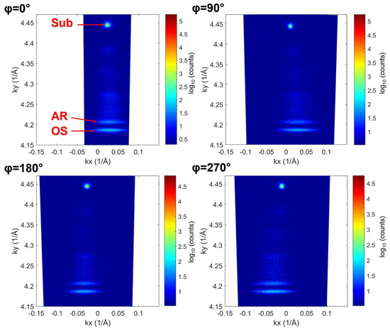
Figure 6.
Symmetric (004) RSMs of sample E at φ = 0°/180° and 90°/270° sample azimuths, with scattering planes parallel to and [110] directions, respectively.
We assess the strain state of the structure from the RSMs near the 224 asymmetric nodes. Figure 7 shows asymmetric (224) RSMs of sample E measured at azimuthal angles φ = 0° and φ = 90°, around (2–24) and (224) reciprocal lattice vectors, respectively. Figure 7 (left picture) shows the AR peak aligned along the (224) reciprocal lattice vector of the GaAs substrate, indicating a strain-free AR layer in the [110] direction. We also observe that (224) AR and OS peaks are vertically aligned, indicating a parallel lattice match between the AR and OS layers. We thus conclude that the OS layer is in a compressive state in this direction.
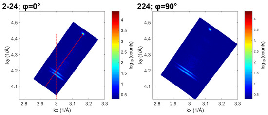
Figure 7.
Asymmetric (224) RSMs of sample E at φ = 0° and 90° sample azimuths, with scattering planes parallel to and [110] directions, respectively. In the φ = 0° RSM, the AR and substrate peaks are aligned along the (224) scattering vector (red arrow), and the AR and OS peaks are aligned along the vertical direction (dashed line).
We obtained the parallel and perpendicular lattice parameters apar and aperp from the kx (=kpar) and ky (=kperp) positions of the OS and AR peaks in the RSMs. The parallel and perpendicular strain εpar and εperp of AR and OS layers can then be calculated as ε par/perp = (a par/perp−arelaxed)/arelaxed. The substrate miscut and the epilayer tilt were corrected for by averaging the peak positions between RSMs measured with azimuthal angles differing by 180°. We calculated the relaxed lattice parameters using the InAs Poisson ratio ν = 0.352, according to arelaxed = aperp × (1 + ν)/(1 − ν) + apar × 2ν/(1 − ν), where apar was averaged between the [110] and directions. We also estimated the In fraction in both OS and AR following Vegard’s law. The results are consistent with the nominal values. The data are summarized in Table 1.

Table 1.
Lattice parameters a, residual strain ε, and In fraction xIn in Sample E.
Hence, anisotropy is observed in the strain relaxation of the AR region, with negligible strain along the direction and tensile strain along the [110] direction. The εperp value of the AR (–0.0016) agrees with the data reported in Figure 5b. This anisotropy correlates with the higher dislocation density along the [110] direction, corresponding to more misfit dislocation lines parallel to the direction [30,31,32]. Two types of perfect dislocations with Burgers vector b = a/2(110) exist in III–V compound semiconductors, known as α and β types. The nucleation and gliding of α and β dislocations control the relaxation along the [110] and directions. Due to the different core structures of these dislocations, there is a significant difference in activation energy for dislocation nucleation and glide. This behavior of dislocation motion is responsible for the observed strain relaxation anisotropy.
We determine the two-dimensional (2D) electron density (Ns) and mobility (µ) of all samples, as shown in Figure 8. Samples are measured in a van der Pauw configuration at 4.2 K. Ns is nearly independent of overshoot layer thickness and lies between 2.3 × 1011 cm−2 and 2.7 × 1011 cm−2. On the other hand, the mobility of samples A, B, C, and D lies in the range of 3.4 × 105 cm2/Vs to 4.4 × 105 cm2/Vs. Sample E has a peak mobility of 5.55 × 105 cm2/Vs with a carrier concentration of 2.4 × 1011 cm−2.
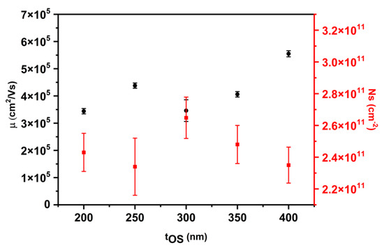
Figure 8.
The 2D electron mobility µ (black symbols) and density Ns (red symbols) of the InAs/InGaAs 2DEGs at 4.2 K as a function of overshoot layer thickness.
The main scattering mechanisms limiting the mobility in undoped InAs/InGaAs QWs are background impurities, interface roughness, and alloy disorder scattering [3,4,16,21]. The most important scattering mechanism in high-mobility QWs is background impurities scattering [4,16]. However, the concentration of background impurities is similar for all samples discussed here because it depends on the MBE system. Furthermore, alloy disorder scattering is comparable for all samples because it is related to the disorder in the ternary alloys of the barriers, which have the same thickness and composition in all samples. The AFM study revealed that all samples show similar RMS roughness. Thus, surface roughness is not the cause of the observed behavior of mobility.
A possible explanation for the lower mobility of samples A to D compared to sample E could be the smaller distance between the QW region and the last misfit dislocations in the buffer layer. The values measured using TEM are (375 ± 10) nm for sample C and (495 ± 5) nm for sample E. In fact, it is well known that dislocations can act as trapping centers and thus create a random electric field inside the material [15,33]. The smaller distance of this random electric field to the well in samples A to D, with respect to sample E, could be a possible cause of the mobility reduction.
Another difference between the samples of the series is the residual strain in the active region layers. Theoretical work has demonstrated that strain affects the mobility of lattice-mismatched QWs due to random fluctuations in the strain field, which produce a fluctuating piezoelectric field [34]. Sample A has a compressively strained active region with the out-of-plane lattice constant of the InAlAs barriers larger than the in-plane lattice constant. Therefore, the pseudomorphically grown InAs QW is compressively strained. Instead, the active regions of the other samples are subject to a tensile strain due to the presence of a thicker and more relaxed overshoot layer. There seems to be, however, no clear inverse correlation between the strain in the active region and the mobility: while samples A and B have the lowest absolute values of strain in the active region, it is sample E that has the highest mobility, despite some tensile strain in the active region. This indicates that a certain amount of tensile strain in the QW promotes mobility. Indeed, it is well known that the bandgap of InAs reduces under the influence of tensile strain [35,36]. Strain also affects the effective mass of the material [35,36]; due to the reduction of bandgap, the effective mass also decreases. Since carrier mobility is inversely proportional to the carrier’s effective masses, a reduction in the effective mass will lead to an increase in mobility.
A possible anisotropy in mobility is investigated by fabricating Hall-bar devices on the highest mobility sample E. Specifically, HBs were aligned along the and [110] directions. Ns and µ were measured at 2.6 K via the Hall effect. We measured four HBs in both crystallographic directions. The measured average value of Ns along the [110] direction is (2.33 ± 0.08) × 1011 cm−2, while along the direction, it is (2.28 ± 0.03) × 1011 cm−2, in very good agreement with the value of sample E obtained with the van der Pauw method (see Figure 8). On the other hand, the measured average value of µ along the [110] direction is (6.09 ± 0.57) × 105 cm2/Vs, while along the direction, it is (6.04 ± 0.23) × 105 cm2/Vs. Within error bars, the 2D electron density and mobility are identical in both crystallographic directions, even though we observed anisotropy in the undulation period and the strain relaxation in our samples. The average mobilities of sample E, obtained with the van der Pauw method and from Hall-bar devices, are in agreement to be within 10%.
The main reasons for the anisotropy of mobility reported in the literature are interface roughness, indium concentration modulation, asymmetric strain relaxation, anisotropic ordering effects, and anisotropic growth of dislocations [3,5,20,21,23,24]. A large anisotropy of mobility was observed in In1−xGaxAs QWs [3,20,21,23,24]. As demonstrated in Ref. [23], the anisotropy of mobility is strongly affected by indium compositional fluctuations in the In1−xGaxAs QWs system. Also, for 4 nm-thick InAs QWs, an anisotropy was reported [5]. Here, we employ 7 nm-thick QWs, which allows us to increase the fraction of the wave function contained in the binary InAs layer to approximately 70% [16] so that the electrons are less sensitive to the indium compositional fluctuations.
4. Conclusions
In this work, we have grown undoped InAs/In0.81Ga0.19As QW structures on GaAs(100) substrates using step-graded InAlAs metamorphic buffer layers. We have grown a series of samples with different overshoot layer thicknesses to tune the residual strain in the active region. We studied the influence of overshoot layer thickness on morphology, structure, strain, and electrical properties of the undoped InAs/In0.81Ga0.19As QW system. All samples show a crosshatch pattern oriented along the two orthogonal directions, and [110], with an RMS roughness of the sample surface of (3.2 ± 1) nm. The residual strain was studied using XRD rocking curves and RSMs. Interestingly, we observed that the residual strain in the active region is compressive in samples with a 200 nm-thick overshoot layer and tensile in samples with thicker overshoot layers, confirming that the final strain state of the active region can be accurately tailored by the choice of overshoot layer composition and thickness.
In addition, the residual strain in the active region saturates to a constant value for overshoot layer thicknesses above 350 nm. We investigated how the state of relaxation of the active region influences the transport properties of the InAs QWs. The sample with a 400 nm-thick overshoot layer shows a peak electron mobility of 6.07 × 105 cm2/Vs at 2.6 K with a carrier concentration of 2.31 × 1011 cm−2. Furthermore, the sample with the 400 nm-thick overshoot layer shows identical values of 2D electron density and mobility along both crystallographic directions. We attribute this to the strong confinement of the carriers to the inside of the binary InAs QW and a negligible effect of misfit dislocations, which are completely confined to the graded buffer layer. We believe that our study will promote further development of InAs/InxGa1−xAs QW systems for high-speed electronic devices.
Author Contributions
Conceptualization, L.S.; Formal analysis, O.A., L.C., E.F., C.F., L.L. and L.N.; Funding acquisition, L.S.; Investigation, O.A., L.C., E.F., C.F., L.L., L.N., S.H. and L.S.; Project administration, L.S.; Resources, A.P. and L.S.; Supervision, S.H. and L.S.; Validation, S.H. and L.S.; Writing—original draft, O.A.; Writing—review and editing, E.F., C.F., L.L., L.N., A.P., S.H. and L.S. All authors have read and agreed to the published version of the manuscript.
Funding
This research activity was supported by PNRR MUR Project No. PE0000023-NQSTI and by the National Infrastructure of the National Research Council for quantum simulations and calculations “PASQUA”.
Data Availability Statement
Data are contained within the article.
Conflicts of Interest
The authors declare no conflict of interest.
References
- Shen, J.L.; Dai, Y.D.; Chen, Y.F.; Chang, S.Z.; Lee, S.C. Cyclotron-resonance studies in relaxed InxGa1−xAs (0 ≤ x ≤ 1) epilayers. Phys. Rev. B 1995, 51, 17648. [Google Scholar] [CrossRef] [PubMed]
- Malinowski, A.; Guerrier, D.J.; Traynor, N.J.; Harley, R.T. Larmor beats and conduction electron g factors in InxGa1−xAs/GaAs quantum wells. Phys. Rev. B 1999, 60, 7728. [Google Scholar] [CrossRef]
- Capotondi, F.; Biasiol, G.; Ercolani, D.; Sorba, L. Scattering mechanisms in undoped In0.75Ga0.25As/In0.75Al0.25As two-dimensional electron gases. J. Cryst. Growth 2005, 278, 538–543. [Google Scholar] [CrossRef]
- Hatke, A.T.; Wang, T.; Thomas, C.; Gardner, G.C.; Manfra, M.J. Mobility in excess of 106 cm2/Vs in InAs quantum wells grown on lattice mismatched InP substrates. Appl. Phys. Lett. 2017, 111, 142106. [Google Scholar] [CrossRef]
- Strickland, W.M.; Hatefipour, M.; Langone, D.; Farzaneh, S.M.; Shabani, J. Controlling Fermi level pinning in near-surface InAs quantum wells. Appl. Phys. Lett. 2022, 121, 092104. [Google Scholar] [CrossRef]
- Del Alamo, J.A. Nanometre-scale electronics with III–V compound semiconductors. Nature 2011, 479, 317–323. [Google Scholar] [CrossRef] [PubMed]
- Ajayan, J.; Nirmal, D. A review of InP/InAlAs/InGaAs based transistors for high frequency applications. Super. Micro. 2015, 86, 1–19. [Google Scholar] [CrossRef]
- Bailey, C.G.; Forbes, D.V.; Raffaelle, R.P.; Hubbard, S.M. Near 1 V open circuit voltage InAs/GaAs quantum dot solar cells. Appl. Phys. Lett. 2011, 98, 163105. [Google Scholar] [CrossRef]
- Gu, Y.; Chen, X.Y.; Zhang, Y.G.; Cao, Y.Y.; Fang, X.; Li, H.S.B.Y. Type-I mid-infrared InAs/InGaAs quantum well lasers on InP-based metamorphic InAlAs buffers. J. Phys. D Appl. Phys. 2013, 46, 505103. [Google Scholar] [CrossRef]
- Datta, S.; Das, B. Electronic analog of the electro-optic modulator. Appl. Phys. Lett. 1990, 56, 665–667. [Google Scholar] [CrossRef]
- Sütő, M.; Prok, T.; Makk, P.; Kirti, M.; Biasiol, G.; Csonka, S.; Tóvári, E. Near-surface InAs two-dimensional electron gas on a GaAs substrate: Characterization and superconducting proximity effect. Phys. Rev. B 2022, 106, 235404. [Google Scholar] [CrossRef]
- Suominen, H.J.; Kjaergaard, M.; Hamilton, A.R.; Shabani, J.; Palmstrøm, C.J.; Marcus, C.M.; Nichele, F. Zero-energy modes from coalescing Andreev states in a two-dimensional semiconductor-superconductor hybrid platform. Phys. Rev. Lett. 2017, 119, 176805. [Google Scholar] [CrossRef] [PubMed]
- Ramachandran, V.; Schrimpf, R.D.; Reed, R.A.; Zhang, E.; Shen, X.; Pantelides, S.T.; MacMorrow, D.; Boos, J.B. Single-event transient sensitivity to gate bias in InAlSb/InAs/AlGaSb high electron mobility transistors. In Proceedings of the 2012 International Conference on Indium Phosphide and Related Materials, Santa Barbara, CA, USA, 27–30 August 2012; pp. 77–80. [Google Scholar] [CrossRef]
- Predan, F.; Ohlmann, J.; Mrabet, S.; Dimroth, F.; Lackner, D. Hall characterization of epitaxial GaSb and AlGaAsSb layers using pn junctions on GaSb substrates. J. Cryst. Growth 2018, 496, 36–42. [Google Scholar] [CrossRef]
- Capotondi, F.; Biasiol, G.; Ercolani, D.; Grillo, V.; Carlino, E.; Romanato, F.; Sorba, L. Strain induced effects on the transport properties of metamorphic InAlAs/InGaAs quantum wells. Thin Solid Films 2005, 484, 400–407. [Google Scholar] [CrossRef]
- Benali, A.; Rajak, P.; Ciancio, R.; Plaisier, J.R.; Heun, S.; Biasiol, G. Metamorphic InAs/InGaAs QWs with electron mobilities exceeding 7 × 105 cm2/Vs. J. Cryst. Growth 2022, 593, 126768. [Google Scholar] [CrossRef]
- Komissarova, T.A.; Chernov, M.Y.; Solov’ev, V.A.; Meltser, B.Y.; Brunkov, P.N.; Sitnikova, A.A.; Kop’ev, P.S.; Ivanov, S.V. Electrical and optical properties of convex-type metamorphic In0.75Ga0.25As/In0.7Al0.3As quantum well structures grown by MBE on GaAs. Mater. Res. Express 2017, 4, 105902. [Google Scholar] [CrossRef]
- Chen, X.Y.; Gu, Y.; Zhang, Y.G.; Ma, Y.J.; Du, B.; Zhang, J.; Ji, W.Y.; Shi, Y.H.; Zhu, Y. Growth temperature optimization of GaAs-based In0.83Ga0.17As on InxAl1−xAs buffers. J. Cryst. Growth 2018, 488, 51–56. [Google Scholar] [CrossRef]
- Solov’ev, V.A.; Chernov, M.Y.; Sitnikova, A.A.; Brunkov, P.N.; Meltser, B.Y.; Ivanov, S.V. Optimization of the Structural Properties and Surface Morphology of a Convex-Graded InxAl1–xAs (x = 0.05–0.83) Metamorphic Buffer Layer Grown via MBE on GaAs (001). Semiconductors 2018, 52, 120–125. [Google Scholar] [CrossRef]
- Chen, C.; Farrer, I.; Holmes, S.N.; Sfigakis, F.; Fletcher, M.P.; Beere, H.E.; Ritchie, D.A. Growth variations and scattering mechanisms in metamorphic In0.75Ga0.25As/In0.75Al0.25As quantum wells grown by molecular beam epitaxy. J. Cryst. Growth 2015, 425, 70–75. [Google Scholar] [CrossRef]
- Ramvall, P.; Carlsson, N.; Omling, P.; Samuelson, L.; Seifert, W.; Wang, Q.; Ishibashi, K.; Aoyagi, Y. Quantum transport in high mobility modulation doped Ga0.25In0.75As/InP quantum wells. J. Appl. Phys. 1998, 84, 2112–2122. [Google Scholar] [CrossRef]
- Shabani, J.; Sarma, S.D.; Palmstrøm, C.J. An apparent metal-insulator transition in high-mobility two-dimensional InAs heterostructures. Phys. Rev. B 2014, 90, 161303. [Google Scholar] [CrossRef]
- Ercolani, D.; Biasiol, G.; Cancellieri, E.; Rosini, M.; Jacoboni, C.; Carillo, F.; Heun, S.; Sorba, L.; Nolting, F. Transport anisotropy in In0.75Ga0.25As two-dimensional electron gases induced by indium concentration modulation. Phys. Rev. B 2008, 77, 235307. [Google Scholar] [CrossRef]
- Kulbachinskii, V.A.; Oveshnikov, L.N.; Lunin, R.A.; Yuzeeva, N.A.; Galiev, G.B.; Klimov, E.A.; Pushkarev, S.S.; Maltsev, P.P. Influence of buffer-layer construction and substrate orientation on the electron mobilities in metamorphic In0.70Al0.30As/In0.76Ga0.24As/In0.70Al0.30As structures on GaAs substrates. Semiconductors 2015, 49, 921–929. [Google Scholar] [CrossRef]
- Capotondi, F.; Biasiol, G.; Vobornik, I.; Sorba, L.; Giazotto, F.; Cavallini, A.; Fraboni, B. Two-dimensional electron gas formation in undoped In0.75Ga0.25As/In0.75Al0.25As quantum wells. J. Vac. Sci. Technol. B 2004, 22, 702–706. [Google Scholar] [CrossRef]
- Pinnington, T.; Lavoie, C.; Tiedje, T. Effect of growth conditions on surface roughening of relaxed InGaAs on GaAs. J. Vac. Sci. Technol. B 1997, 15, 1265–1269. [Google Scholar] [CrossRef]
- Ferrari, C.; Gennari, S.; Franchi, S.; Lazzarini, L.; Natali, M.; Romanato, F.; Drigo, A.V.; Baruchel, J. Investigation by synchrotron radiation X-ray topography of lattice tilt formation in partially released InGaAs/GaAs compositionally graded layers. J. Cryst. Growth 1999, 205, 474–480. [Google Scholar] [CrossRef]
- Lee, D.; Park, M.S.; Tang, Z.; Luo, H.; Beresford, R.; Wie, C.R. Characterization of metamorphic InxAl1−xAs∕GaAs buffer layers using reciprocal space mapping. J. Appl. Phys. 2007, 101, 063523. [Google Scholar] [CrossRef]
- Loke, W.K.; Tan, K.H.; Wicaksono, S.; Yoon, S.F.; Wang, W.; Zhou, Q.; Yeo, Y.C. Strain-relaxed buffer technology based on metamorphic InxAl1-xAs. J. Cryst. Growth 2015, 424, 68–76. [Google Scholar] [CrossRef]
- Hudait, M.K.; Lin, Y.; Palmisiano, M.N.; Tivarus, C.; Pelz, J.P.; Ringel, S.A. Comparison of mixed anion, InAsyP1−y and mixed cation, InxAl1−xAs metamorphic buffers grown by molecular beam epitaxy on (100) InP substrates. J. Appl Phys. 2004, 95, 3952–3960. [Google Scholar] [CrossRef]
- Jiang, Z.; Wang, W.; Gao, H.; Liu, L.; Chen, H.; Zhou, J. Strain relaxation and surface morphology of high indium content InAlAs metamorphic buffers with reverse step. Appl. Surf. Sci. 2008, 254, 5241–5246. [Google Scholar] [CrossRef]
- Solov’ev, V.A.; Chernov, M.Y.; Baidakova, M.V.; Kirilenko, D.A.; Yagovkina, M.A.; Sitnikova, A.A.; Komissarova, T.A.; Kop’ev, P.S.; Ivanov, S.V. Strain relaxation in convex-graded InxAl1−xAs (x = 0.05–0.79) metamorphic buffer layers grown by molecular beam epitaxy on GaAs (001). Super. Micro. 2018, 113, 777–784. [Google Scholar] [CrossRef]
- Woodall, J.M.; Pettit, G.D.; Jackson, T.N.; Lanza, C.; Kavanagh, K.L.; Mayer, J.W. Fermi-level pinning by misfit dislocations at GaAs interfaces. Phys. Rev. Lett. 1983, 51, 1783. [Google Scholar] [CrossRef]
- Quang, D.N.; Tuoc, V.N.; Huan, T.D. Roughness-induced piezoelectric scattering in lattice-mismatched semiconductor quantum wells. Phys. Rev. B 2003, 68, 195316. [Google Scholar] [CrossRef]
- Pryor, C.E.; Pistol, M.-E. Band-edge diagrams for strained III–V semiconductor quantum wells, wires, and dots. Phys. Rev. B 2005, 72, 205311. [Google Scholar] [CrossRef]
- Jain, N.; Mal, I.; Samajdar, D.P.; Bagga, N. Theoretical exploration of the optoelectronic properties of InAsNBi/InAs heterostructures for infrared applications: A multi-band k·p approach. Mater. Sci. Semi. Proc. 2022, 148, 106822. [Google Scholar] [CrossRef]


Disclaimer/Publisher’s Note: The statements, opinions and data contained in all publications are solely those of the individual author(s) and contributor(s) and not of MDPI and/or the editor(s). MDPI and/or the editor(s) disclaim responsibility for any injury to people or property resulting from any ideas, methods, instructions or products referred to in the content. |
© 2024 by the authors. Licensee MDPI, Basel, Switzerland. This article is an open access article distributed under the terms and conditions of the Creative Commons Attribution (CC BY) license (https://creativecommons.org/licenses/by/4.0/).