
Enhancing Charge Trapping Performance of Hafnia Thin Films Using Sequential Plasma Atomic Layer Deposition

 ,
, 
Abstract
1. Introduction
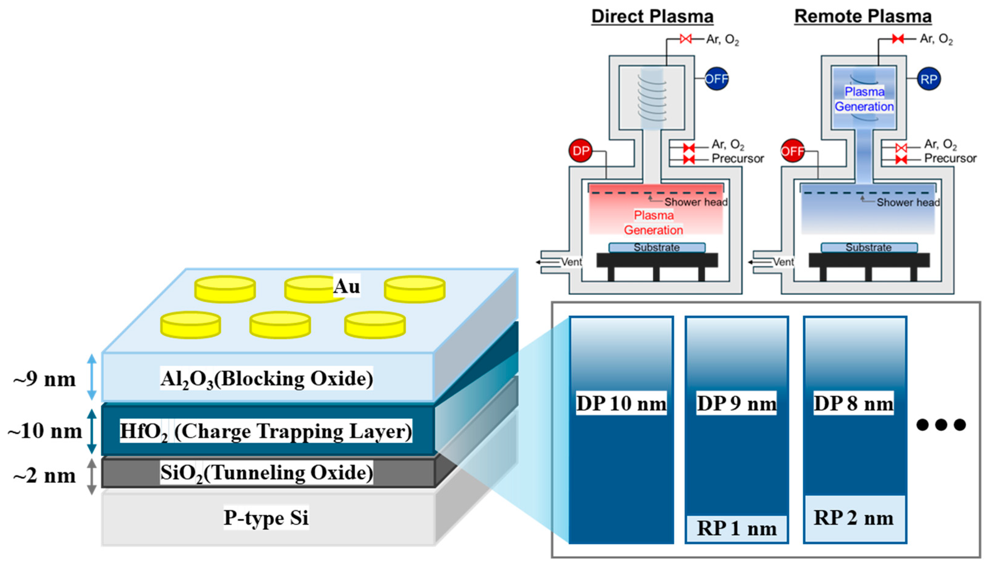
2. Materials and Methods
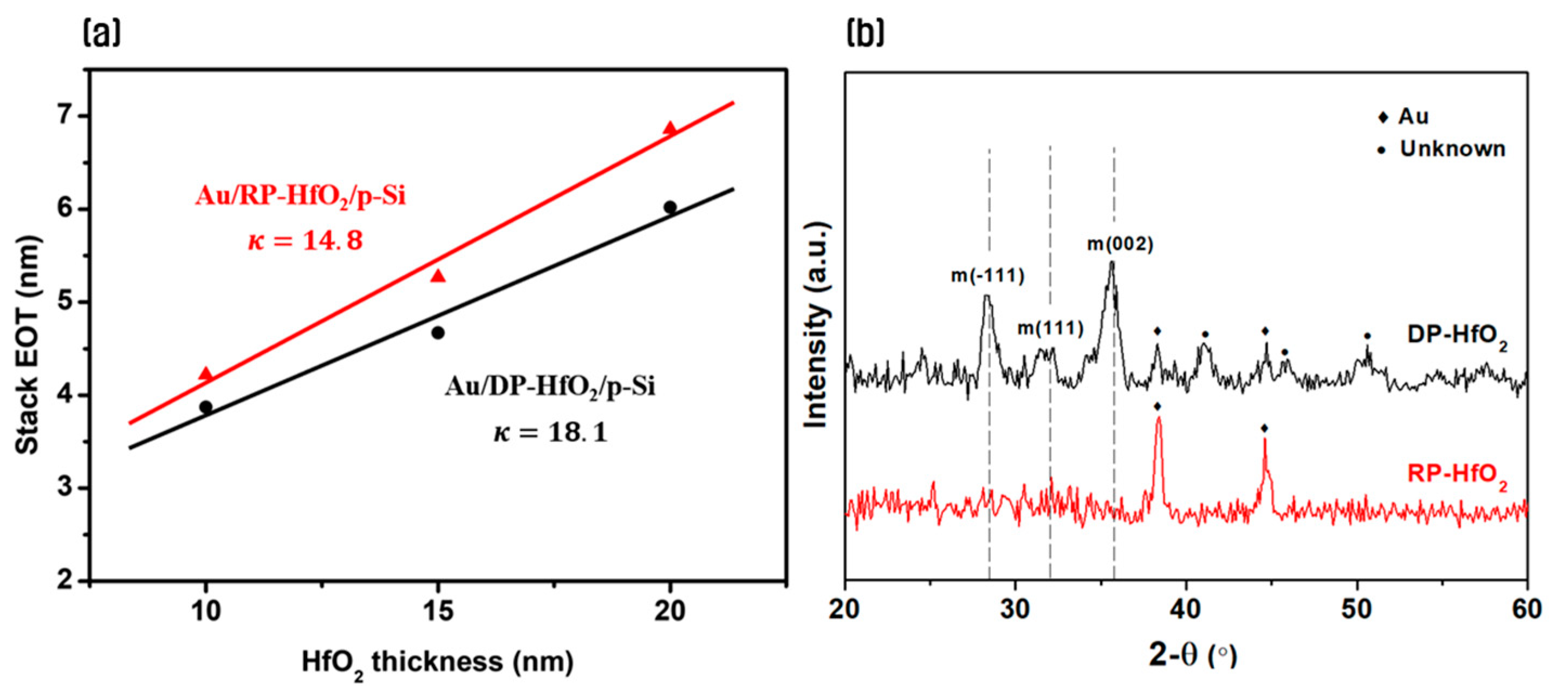
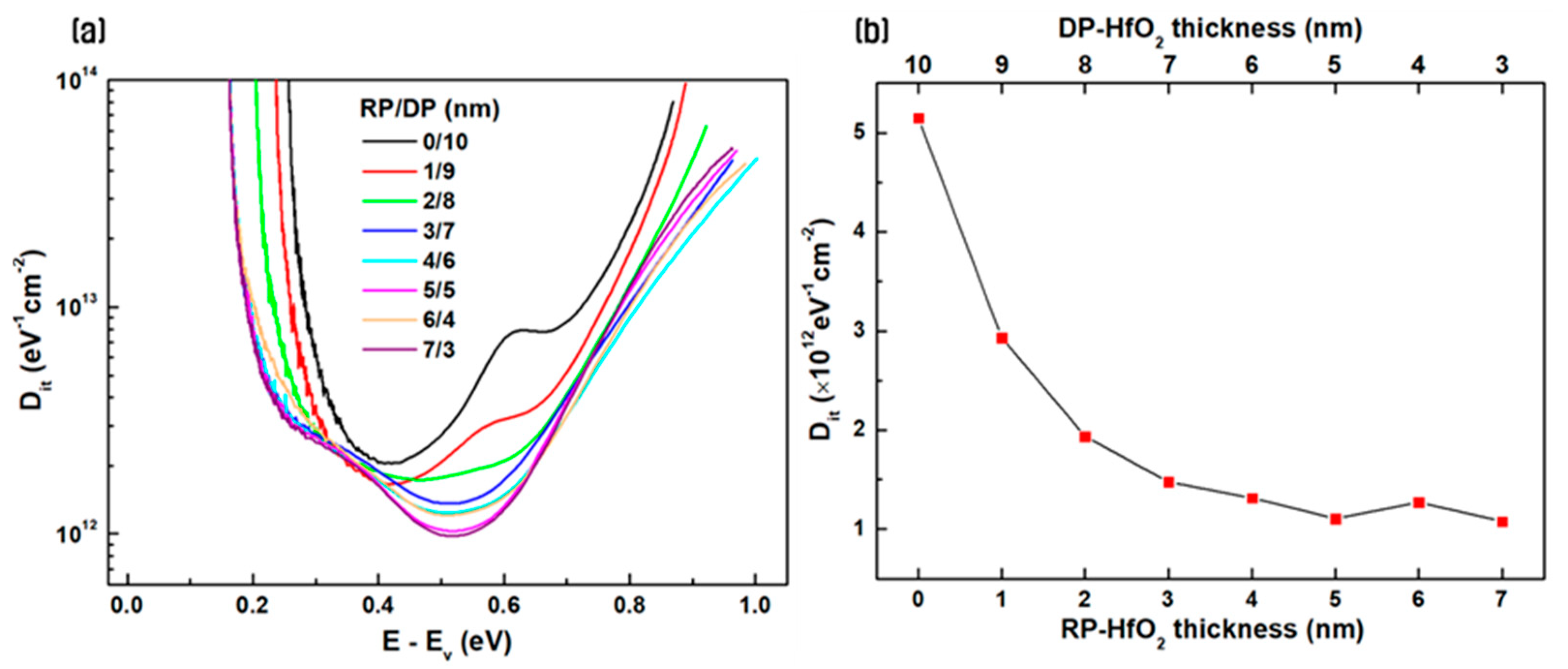
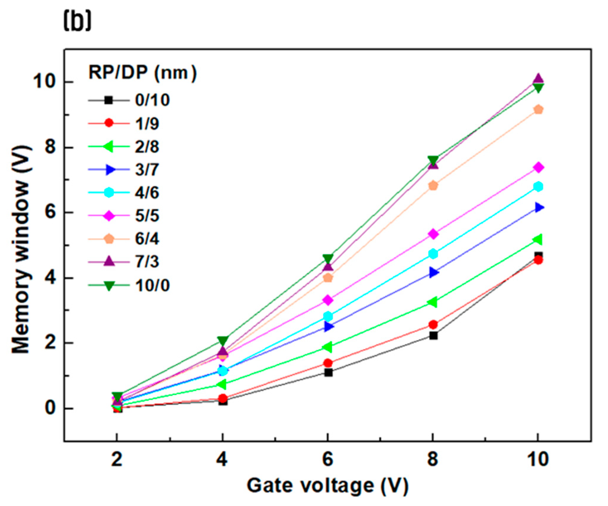
3. Results and Discussion
4. Conclusions
Author Contributions
Funding
Data Availability Statement
Conflicts of Interest
References
- Böscke, T.S.; Müller, J.; Bräuhaus, D.; Schröder, U.; Böttger, U. Ferroelectricity in Hafnium Oxide Thin Films. Appl. Phys. Lett. 2011, 99, 102903. [Google Scholar] [CrossRef]
- Park, M.H.; Lee, Y.H.; Mikolajick, T.; Schroeder, U.; Hwang, C.S. Review and Perspective on Ferroelectric HfO2-Based Thin Films for Memory Applications. MRS Commun. 2018, 8, 795–808. [Google Scholar] [CrossRef]
- Liao, J.; Dai, S.; Peng, R.C.; Yang, J.; Zeng, B.; Liao, M.; Zhou, Y. HfO2-Based Ferroelectric Thin Film and Memory Device Applications in the Post-Moore Era: A Review. Fundam. Res. 2023, 3, 332–345. [Google Scholar] [CrossRef]
- Han, S.T.; Zhou, Y.; Roy, V.A.L. Towards the Development of Flexible Non-Volatile Memories. Adv. Mater. 2013, 25, 5425–5449. [Google Scholar] [CrossRef] [PubMed]
- Ni, Y.; Wang, Y.; Xu, W. Recent Process of Flexible Transistor-Structured Memory. Small 2021, 17, 1–23. [Google Scholar] [CrossRef] [PubMed]
- Kim, D.H.; Cho, S.; Li, D.H.; Yun, J.G.; Lee, J.H.; Lee, G.S.; Kim, Y.; Shim, W.B.; Park, S.H.; Kim, W.; et al. Program/Erase Model of Nitride-Based NAND-Type Charge Trap Flash Memories. Jpn. J. Appl. Phys. 2010, 49, 084301. [Google Scholar] [CrossRef]
- Choi, B.; Lee, J.; Yoon, J.; Jeon, M.; Lee, Y.; Han, J.; Lee, J.; Park, J.; Kim, Y.; Kim, D.M.; et al. Effect of Charge Trap Layer Thickness on the Charge Spreading Behavior within a Few Seconds in 3D Charge Trap Flash Memory. Semicond. Sci. Technol. 2018, 33, 1–5. [Google Scholar] [CrossRef]
- Lee, G.H.; Hwang, S.; Yu, J.; Kim, H. Architecture and Process Integration Overview of 3d Nand Flash Technologies. Appl. Sci. 2021, 11, 6703. [Google Scholar] [CrossRef]
- You, H.W.; Cho, W.J. Charge Trapping Properties of the HfO2 Layer with Various Thicknesses for Charge Trap Flash Memory Applications. Appl. Phys. Lett. 2010, 96, 94–97. [Google Scholar] [CrossRef]
- Zhang, Y.; Shao, Y.Y.; Lu, X.B.; Zeng, M.; Zhang, Z.; Gao, X.S.; Zhang, X.J.; Liu, J.M.; Dai, J.Y. Defect States and Charge Trapping Characteristics of HfO2 Films for High Performance Nonvolatile Memory Applications. Appl. Phys. Lett. 2014, 105, 172902. [Google Scholar] [CrossRef]
- Wang, J.; Bi, J.; Xu, Y.; Niu, G.; Liu, M.; Stempitsky, V. Effects of Charge Trapping on Memory Characteristics for HfO2-Based Ferroelectric Field Effect Transistors. Nanomaterials 2023, 13, 638. [Google Scholar] [CrossRef]
- Profijt, H.B.; Potts, S.E.; van de Sanden, M.C.M.; Kessels, W.M.M. Plasma-Assisted Atomic Layer Deposition: Basics, Opportunities, and Challenges. J. Vac. Sci. Technol. A Vac. Surf. Film. 2011, 29, 050801. [Google Scholar] [CrossRef]
- Knoops, H.C.M.; Faraz, T.; Arts, K.; Kessels, W.M.M. (Erwin) Status and Prospects of Plasma-Assisted Atomic Layer Deposition. J. Vac. Sci. Technol. A Vac. Surf. Film. 2019, 37, 030902. [Google Scholar] [CrossRef]
- Lee, H.R.; Beom, K.W.; Kim, M.J.; Yoon, T.S. Post-annealing temperature-dependent electrical properties of thin-film transistors with ZnO channel and HfOx gate insulator deposited by atomic layer deposition. Semicond. Sci. Technol. 2020, 35, 075013. [Google Scholar] [CrossRef]
- Han, J.; Jeong, B.; Sahu, D.P.; Kim, H.M.; Yoon, T.S. Non-Volatile Charge-Trap Memory Characteristics with Low-Temperature Atomic Layer Deposited HfO2−x Charge-Trap Layer and Interfacial Tunneling Oxide Formed by UV/Ozone Treatment. J. Alloys Compd. 2023, 951, 169858. [Google Scholar] [CrossRef]
- Yoo, J.H.; Park, W.J.; Kim, S.W.; Lee, G.R.; Kim, J.H.; Lee, J.H.; Uhm, S.H.; Lee, H.C. Preparation of Remote Plasma Atomic Layer-Deposited HfO2 Thin Films with High Charge Trapping Densities and Their Application in Nonvolatile Memory Devices. Nanomaterials 2023, 13, 1785. [Google Scholar] [CrossRef] [PubMed]
- Profijt, H.B.; Kessels, W.M.M. Ion Bombardment during Plasma-Assisted Atomic Layer Deposition. ECS Trans. 2012, 50, 23–34. [Google Scholar] [CrossRef]
- Oh, I.K.; Yoo, G.; Yoon, C.M.; Kim, T.H.; Yeom, G.Y.; Kim, K.; Lee, Z.; Jung, H.; Lee, C.W.; Kim, H.; et al. Very High Frequency Plasma Reactant for Atomic Layer Deposition. Appl. Surf. Sci. 2016, 387, 109–117. [Google Scholar] [CrossRef]
- Kim, K.; Oh, I.K.; Kim, H.; Lee, Z. Atomic-Scale Characterization of Plasma-Induced Damage in Plasma-Enhanced Atomic Layer Deposition. Appl. Surf. Sci. 2017, 425, 781–787. [Google Scholar] [CrossRef]
- Yuan, G.; Li, H.; Shan, B.; Liu, J. Critical Atomic-Level Processing Technologies: Remote Plasma-Enhanced Atomic Layer Deposition and Atomic Layer Etching. Micro Nanosyst. 2018, 10, 76–83. [Google Scholar] [CrossRef]
- Cho, H.; Lee, N.; Choi, H.; Park, H.; Jung, C.; Song, S.; Yuk, H.; Kim, Y.; Kim, J.W.; Kim, K.; et al. Remote Plasma Atomic Layer Deposition of SiNx Using Cyclosilazane and H2/N2 Plasma. Appl. Sci. 2019, 9, 3531. [Google Scholar] [CrossRef]
- Khosla, R.; Schwarz, D.; Funk, H.S.; Guguieva, K.; Schulze, J. High-Quality Remote Plasma Enhanced Atomic Layer Deposition of Aluminum Oxide Thin Films for Nanoelectronics Applications. Solid. State. Electron. 2021, 185, 108027. [Google Scholar] [CrossRef]
- Kim, H.K.; Yu, I.H.; Lee, J.H.; Park, T.J.; Seong Hwang, C. Scaling of Equivalent Oxide Thickness of Atomic Layer Deposited HfO2 Film Using RuO2 Electrodes Suppressing the Dielectric Dead-Layer Effect. Appl. Phys. Lett. 2012, 101, 1–6. [Google Scholar] [CrossRef]
- Cheng, Y.L.; Hsieh, C.Y.; Chang, Y.L. Deposition Cycle of Atomic Layer Deposition HfO2 Film: Effects on Electrical Performance and Reliability. Thin Solid Films 2013, 528, 77–81. [Google Scholar] [CrossRef]
- Hackley, J.C.; Gougousi, T. Properties of Atomic Layer Deposited HfO2 Thin Films. Thin Solid Films 2009, 517, 6576–6583. [Google Scholar] [CrossRef]
- Li, S.; Zhang, Y.; Yang, D.; Yang, W.; Chen, X.; Zhao, H.; Hou, J.; Yang, P. Structure and Optical Properties of HfO2 Films on Si (100) Substrates Prepared by ALD at Different Temperatures. Phys. B Condens. Matter 2020, 584, 412065. [Google Scholar] [CrossRef]
- Jung, J.S.; Kwon, J.Y.; Xianyu, W.; Noguchi, T.; Jeong, S.H.; Jeong, S.W.; Roh, Y.; Noguchi, T. Study of HfO2 High-k Gate Oxide for Low-Temperature Poly-Si TFT. J. Korean Phys. Soc. 2006, 48, 32–34. [Google Scholar]
- Migita, S.; Morita, Y.; Mizubayashi, W.; Ota, H. Preparation of Epitaxial HfO2 Film (EOT = 0.5 nm) on Si Substrate Using Atomic-Layer Deposition of Amorphous Film and Rapid Thermal Crystallization (RTC) in an Abrupt Temperature Gradient. In Proceedings of the 2010 International Electron Devices Meeting, San Francisco, CA, USA, 6–8 December 2010; pp. 269–272. [Google Scholar] [CrossRef]
- Mannequin, C.; Gonon, P.; Vallée, C.; Latu-Romain, L.; Bsiesy, A.; Grampeix, H.; Salaün, A.; Jousseaume, V. Stress-Induced Leakage Current and Trap Generation in HfO2 Thin Films. J. Appl. Phys. 2012, 112, 074103. [Google Scholar] [CrossRef]
- Cheema, S.S.; Shanker, N.; Wang, L.C.; Hsu, C.H.; Hsu, S.L.; Liao, Y.H.; San Jose, M.; Gomez, J.; Chakraborty, W.; Li, W.; et al. Ultrathin Ferroic HfO2–ZrO2 Superlattice Gate Stack for Advanced Transistors. Nature 2022, 604, 65–71. [Google Scholar] [CrossRef]
- Engel-Herbert, R.; Hwang, Y.; Stemmer, S. Comparison of Methods to Quantify Interface Trap Densities at Dielectric/III-V Semiconductor Interfaces. J. Appl. Phys. 2010, 108, 124101. [Google Scholar] [CrossRef]
- Del Prado, A.; San Andrés, E.; Mártil, I.; González-Díaz, G.; Kliefoth, K.; Füssel, W. Annealing Effects on the Interface and Insulator Properties of Plasma-Deposited Al/SiOxNyHz/Si Devices. Semicond. Sci. Technol. 2004, 19, 133–141. [Google Scholar] [CrossRef]
- Lee, W.; Oh, J.; Hwan, J.; Choi, S.; Kang, T.; Chu, H.; Kim, H. Comparative Study of C-V-Based Extraction Methods of Interface State Density for a Low-Temperature Polysilicon Thin Film. Mater. Res. Express 2021, 8, 085902. [Google Scholar] [CrossRef]
- Gong, N.; Ma, T.P. A Study of Endurance Issues in HfO2-Based Ferroelectric Field Effect Transistors: Charge Trapping and Trap Generation. IEEE Electron. Device Lett. 2018, 39, 15–18. [Google Scholar] [CrossRef]
- Gong, C.; Yin, Q.; Ou, X.; Lan, X.; Liu, J.; Sun, C.; Wang, L.; Lu, W.; Yin, J.; Xu, B.; et al. The Dominant Factors Affecting the Memory Characteristics of (Ta2O5)x(Al2O3)1−x High-k Charge-Trapping Devices. Appl. Phys. Lett. 2014, 105, 3–8. [Google Scholar] [CrossRef]
- An, H.M.; Kim, H.D.; Kim, T.G. Analysis of the Energy Distribution of Interface Traps Related to Tunnel Oxide Degradation Using Charge Pumping Techniques for 3D NAND Flash Applications. Mater. Res. Bull. 2013, 48, 5084–5087. [Google Scholar] [CrossRef]
- Lan, X.; Ou, X.; Cao, Y.; Tang, S.; Gong, C.; Xu, B.; Xia, Y.; Yin, J.; Li, A.; Yan, F.; et al. The Effect of Thermal Treatment Induced Inter-Diffusion at the Interfaces on the Charge Trapping Performance of HfO2/Al2O3 Nanolaminate-Based Memory Devices. J. Appl. Phys. 2013, 114, 044104. [Google Scholar] [CrossRef]
- Spassov, D.; Paskaleva, A. Challenges to Optimize Charge Trapping Non-Volatile Flash Memory Cells: A Case Study of HfO2/Al2O3 Nanolaminated Stacks. Nanomaterials 2023, 13, 2456. [Google Scholar] [CrossRef]
- Ding, P.; Yang, Y.; Wang, Y.; Liu, C.; Yin, J.; Xia, Y.; Li, A.; Liu, Z. Band-Alignment Dominated Retention Behaviors in High-k Composite Charge-Trapping Memory Devices. Appl. Phys. Lett. 2019, 114, 053506. [Google Scholar] [CrossRef]
- Martínez-Puente, M.A.; Horley, P.; Aguirre-Tostado, F.S.; López-Medina, J.; Borbón-Nuñez, H.A.; Tiznado, H.; Susarrey-Arce, A.; Martínez-Guerra, E. ALD and PEALD Deposition of HfO2 and Its Effects on the Nature of Oxygen Vacancies. Mater. Sci. Eng. B 2022, 285, 115964. [Google Scholar] [CrossRef]
- Kim, S.; Woo, S.; Kim, H.; Kim, I.; Lee, K.; Jeong, W.; Park, T.; Jeon, H. Atomic Layer Deposition of HfO2 Thin Films on Ultrathin SiO2 Formed by Remote Plasma Oxidation. J. Korean Phys. Soc. 2008, 52, 1103–1108. [Google Scholar] [CrossRef]
- Arreghini, A.; Zahid, M.B.; Van Den Bosch, G.; Suhane, A.; Breuil, L.; Cacciato, A.; Van Houdt, J. Effect of High Temperature Annealing on Tunnel Oxide Properties in TANOS Devices. Microelectron. Eng. 2011, 88, 1155–1158. [Google Scholar] [CrossRef]
- Lun, Z.; Wang, T.; Zeng, L.; Zhao, K.; Liu, X.; Wang, Y.; Kang, J.; Du, G. Simulation on Endurance Characteristic of Charge Trapping Memory. In Proceedings of the 2013 International Conference on Simulation of Semiconductor Processes and Devices (SISPAD), Glasgow, UK, 3–5 September 2013; Volume 2, pp. 292–295. [Google Scholar] [CrossRef]
- Tang, Z.; Zhu, X.; Xu, H.; Xia, Y.; Yin, J.; Liu, Z.; Li, A.; Yan, F. Impact of the Interfaces in the Charge Trap Layer on the Storage Characteristics of ZrO2/Al2O3 Nanolaminate-Based Charge Trap Flash Memory Cells. Mater. Lett. 2013, 92, 21–24. [Google Scholar] [CrossRef]
- Zhao, C.; Zhao, C.Z.; Taylor, S.; Chalker, P.R. Review on Non-Volatile Memory with High-k Dielectrics: Flash for Generation beyond 32 nm. Materials 2014, 7, 5117–5145. [Google Scholar] [CrossRef]
- Hou, Z.Z.; Wang, G.L.; Xiang, J.J.; Yao, J.X.; Wu, Z.H.; Zhang, Q.Z.; Yin, H.X. Improved Operation Characteristics for Nonvolatile Charge-Trapping Memory Capacitors with High-k Dielectrics and SiGe Epitaxial Substrates. Chin. Phys. Lett. 2017, 34, 097304. [Google Scholar] [CrossRef]
- Nedoseka, A. Diagnostics and Prediction of the Residual Life of Welded Structures. Fundam. Eval. Diagn. Welded Struct. 2012, e322–e372. [Google Scholar] [CrossRef]
- Khera, E.A.; Mahata, C.; Imran, M.; Niaz, N.A.; Hussain, F.; Khalil, R.M.A.; Rasheed, U.; SungjunKim, N. Improved Resistive Switching Characteristics of a Multi-Stacked HfO2/Al2O3/HfO2 RRAM Structure for Neuromorphic and Synaptic Applications: Experimental and Computational Study. RSC Adv. 2022, 12, 11649–11656. [Google Scholar] [CrossRef]
- Spassov, D.; Paskaleva, A.; Guziewicz, E.; Wozniak, W.; Stanchev, T.; Ivanov, T.; Wojewoda-Budka, J.; Janusz-Skuza, M. Charge Storage and Reliability Characteristics of Nonvolatile Memory Capacitors with HfO2/Al2O3-Based Charge Trapping Layers. Materials 2022, 15, 6285. [Google Scholar] [CrossRef]
- Maikap, S.; Lee, H.Y.; Wang, T.Y.; Tzeng, P.J.; Wang, C.C.; Lee, L.S.; Liu, K.C.; Yang, J.R.; Tsai, M.J. Charge Trapping Characteristics of Atomic-Layer-Deposited HfO2 Films with Al2O3 as a Blocking Oxide for High-Density Non-Volatile Memory Device Applications. Semicond. Sci. Technol. 2007, 22, 884–889. [Google Scholar] [CrossRef]
- Yoo, J.; Kim, S.; Jeon, W.; Park, A.; Choi, D.; Choi, B. A Study on the Charge Trapping Characteristics of High-k Laminated Traps. IEEE Electron. Device Lett. 2019, 40, 1427–1430. [Google Scholar] [CrossRef]
- Lan, X.; Gong, C.; Ou, X.; Cao, Y.; Sun, C.; Chen, Y.; Xu, B.; Xia, Y.; Li, A.; Yin, J.; et al. Enhancement of the Charge Trapping Performances with HfAlO Composite Oxide Thin Films in SONOS-Type Nonvolatile Memory. Microelectron. Eng. 2015, 133, 88–91. [Google Scholar] [CrossRef]
- Liu, J.; Wang, Q.; Long, S.; Zhang, M.; Liu, M. A Metal/Al2O3/ZrO2/SiO2/Si (MAZOS) Structure for High-Performance Non-Volatile Memory Application. Semicond. Sci. Technol. 2010, 25, 055013. [Google Scholar] [CrossRef]


| TO/CTL/BO | Thickness (nm) | Annealing temp. (˚C) | Operating Voltage (V) | Memory Window (V) | Charge Loss (%) | References |
|---|---|---|---|---|---|---|
| SiOX/RP:DP-HfO2/Al2O3 | 2/7:3/9 | 400 | ±10 | 10.1 | 37 | This work |
| SiOX/RP-HfO2/Al2O3 | 2/9/9 | 400 | ±12 | 12.66 | 34.32 | [16] |
| SiO2/HfO2/Al2O3 | 3/10/10 | 1000 | ±15 | 7.4 | 31 | [50] |
| SiO2/HfAlO/Al2O3 | 3/9/8 | 800 | ±16 | 11.5 | 14.9 | [51] |
| Al2O3/HfAlO/Al2O3 | 2/9/12 | 600 | ±12 | 6.29 | 79 | [52] |
| SiO2/ZrO2/Al2O3 | 5/10/15 | 700 | ±11 | 7.1 | 16 | [53] |
Disclaimer/Publisher’s Note: The statements, opinions and data contained in all publications are solely those of the individual author(s) and contributor(s) and not of MDPI and/or the editor(s). MDPI and/or the editor(s) disclaim responsibility for any injury to people or property resulting from any ideas, methods, instructions or products referred to in the content. |
© 2024 by the authors. Licensee MDPI, Basel, Switzerland. This article is an open access article distributed under the terms and conditions of the Creative Commons Attribution (CC BY) license (https://creativecommons.org/licenses/by/4.0/).
Share and Cite
Kim, S.-W.; Yoo, J.-H.; Park, W.-J.; Lee, C.-H.; Lee, J.-H.; Kim, J.-H.; Uhm, S.-H.; Lee, H.-C. Enhancing Charge Trapping Performance of Hafnia Thin Films Using Sequential Plasma Atomic Layer Deposition. Nanomaterials 2024, 14, 1686. https://doi.org/10.3390/nano14201686
Kim S-W, Yoo J-H, Park W-J, Lee C-H, Lee J-H, Kim J-H, Uhm S-H, Lee H-C. Enhancing Charge Trapping Performance of Hafnia Thin Films Using Sequential Plasma Atomic Layer Deposition. Nanomaterials. 2024; 14(20):1686. https://doi.org/10.3390/nano14201686
Chicago/Turabian StyleKim, So-Won, Jae-Hoon Yoo, Won-Ji Park, Chan-Hee Lee, Joung-Ho Lee, Jong-Hwan Kim, Sae-Hoon Uhm, and Hee-Chul Lee. 2024. "Enhancing Charge Trapping Performance of Hafnia Thin Films Using Sequential Plasma Atomic Layer Deposition" Nanomaterials 14, no. 20: 1686. https://doi.org/10.3390/nano14201686
APA StyleKim, S.-W., Yoo, J.-H., Park, W.-J., Lee, C.-H., Lee, J.-H., Kim, J.-H., Uhm, S.-H., & Lee, H.-C. (2024). Enhancing Charge Trapping Performance of Hafnia Thin Films Using Sequential Plasma Atomic Layer Deposition. Nanomaterials, 14(20), 1686. https://doi.org/10.3390/nano14201686