
Plasma Nitridation Effect on β-Ga2O3 Semiconductors


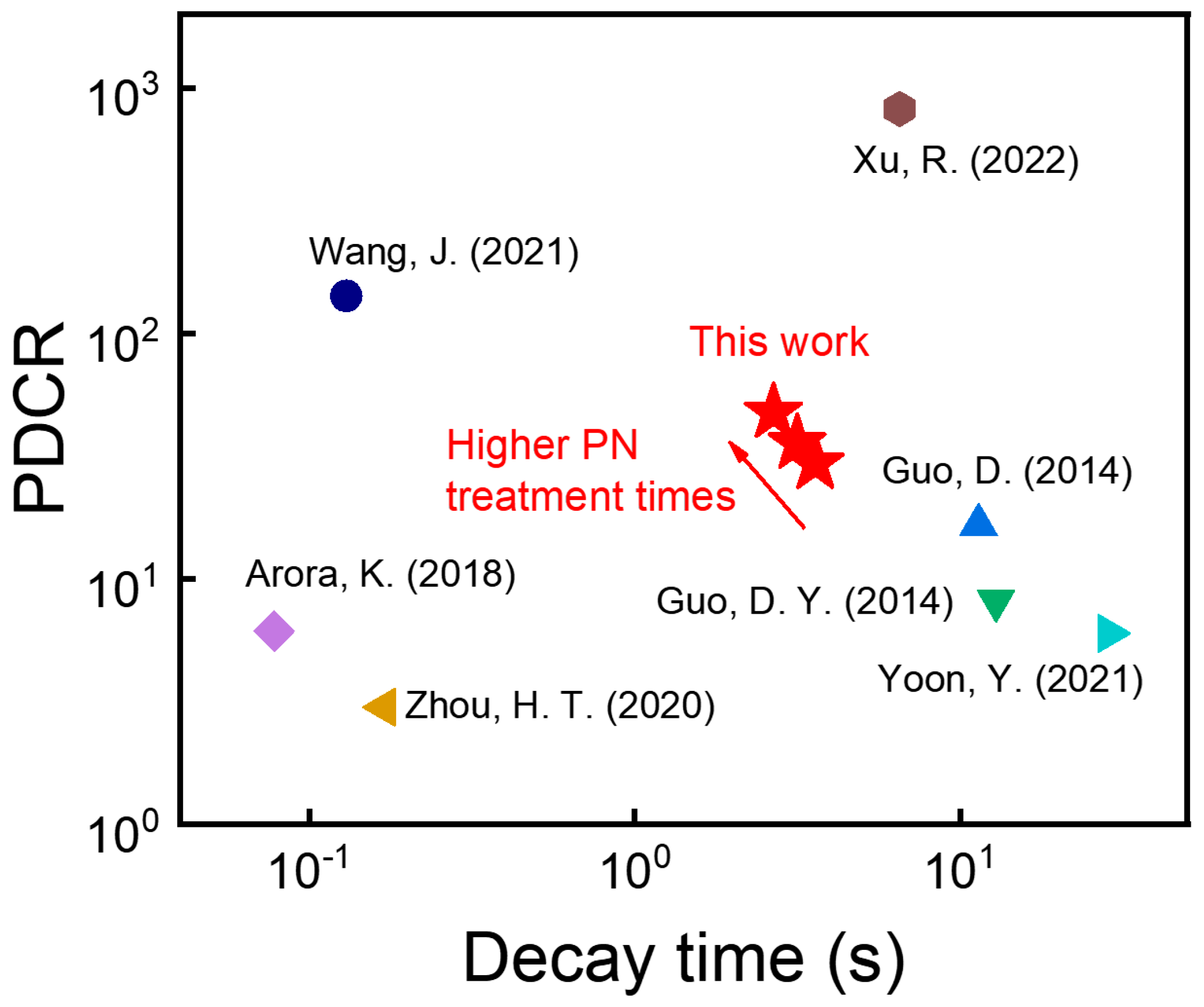
Abstract
Share and Cite
Kim, S.; Kim, M.; Kim, J.; Hwang, W.S. Plasma Nitridation Effect on β-Ga2O3 Semiconductors. Nanomaterials 2023, 13, 1199. https://doi.org/10.3390/nano13071199
Kim S, Kim M, Kim J, Hwang WS. Plasma Nitridation Effect on β-Ga2O3 Semiconductors. Nanomaterials. 2023; 13(7):1199. https://doi.org/10.3390/nano13071199
Chicago/Turabian StyleKim, Sunjae, Minje Kim, Jihyun Kim, and Wan Sik Hwang. 2023. "Plasma Nitridation Effect on β-Ga2O3 Semiconductors" Nanomaterials 13, no. 7: 1199. https://doi.org/10.3390/nano13071199
APA StyleKim, S., Kim, M., Kim, J., & Hwang, W. S. (2023). Plasma Nitridation Effect on β-Ga2O3 Semiconductors. Nanomaterials, 13(7), 1199. https://doi.org/10.3390/nano13071199