

Selected Area Deposition of High Purity Gold for Functional 3D Architectures


Abstract
1. Introduction
2. Methods
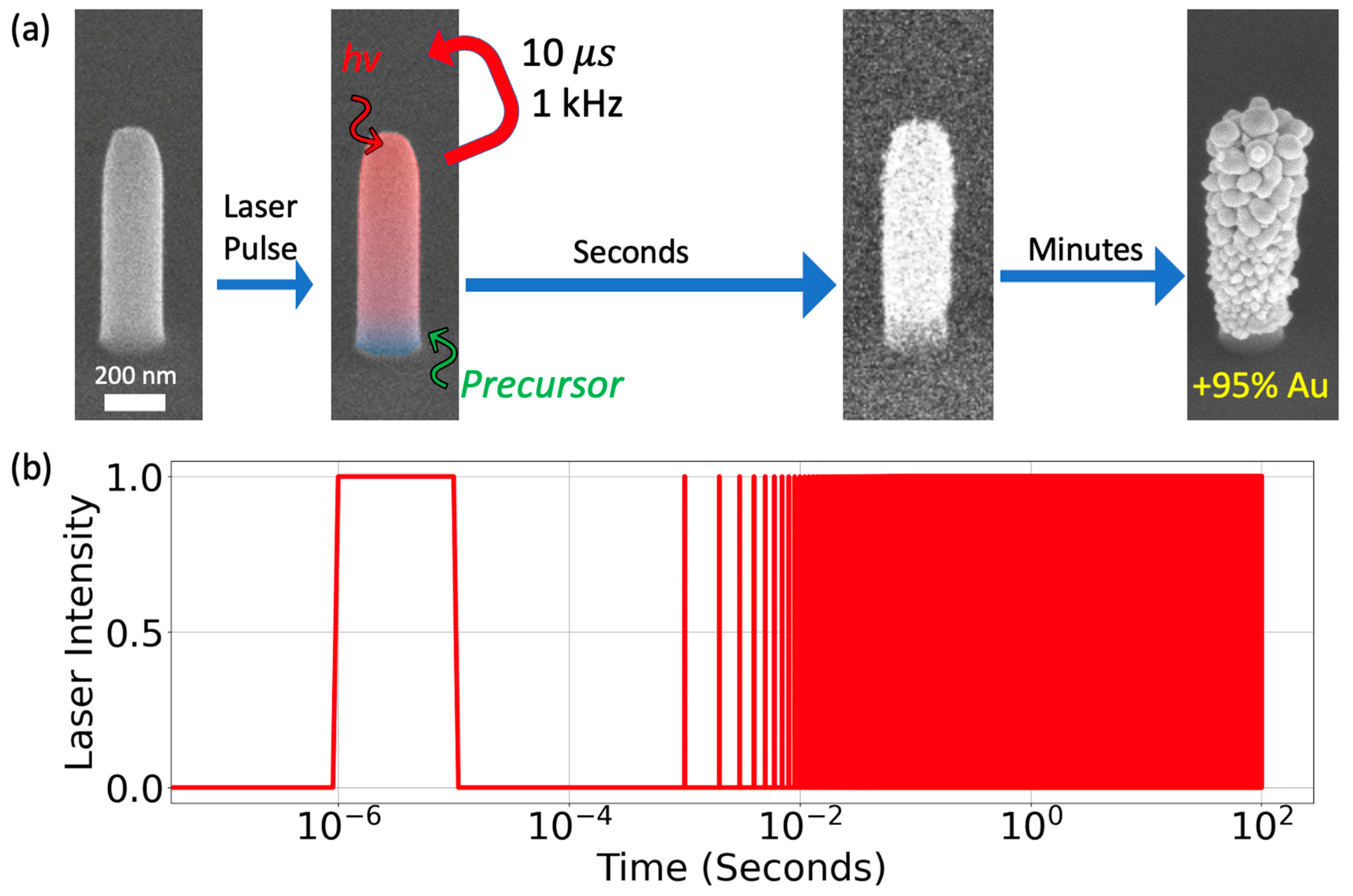
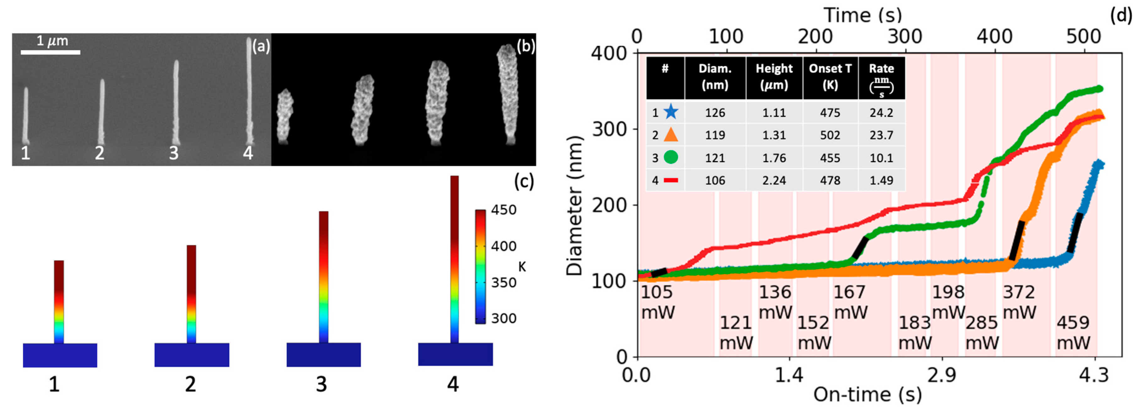
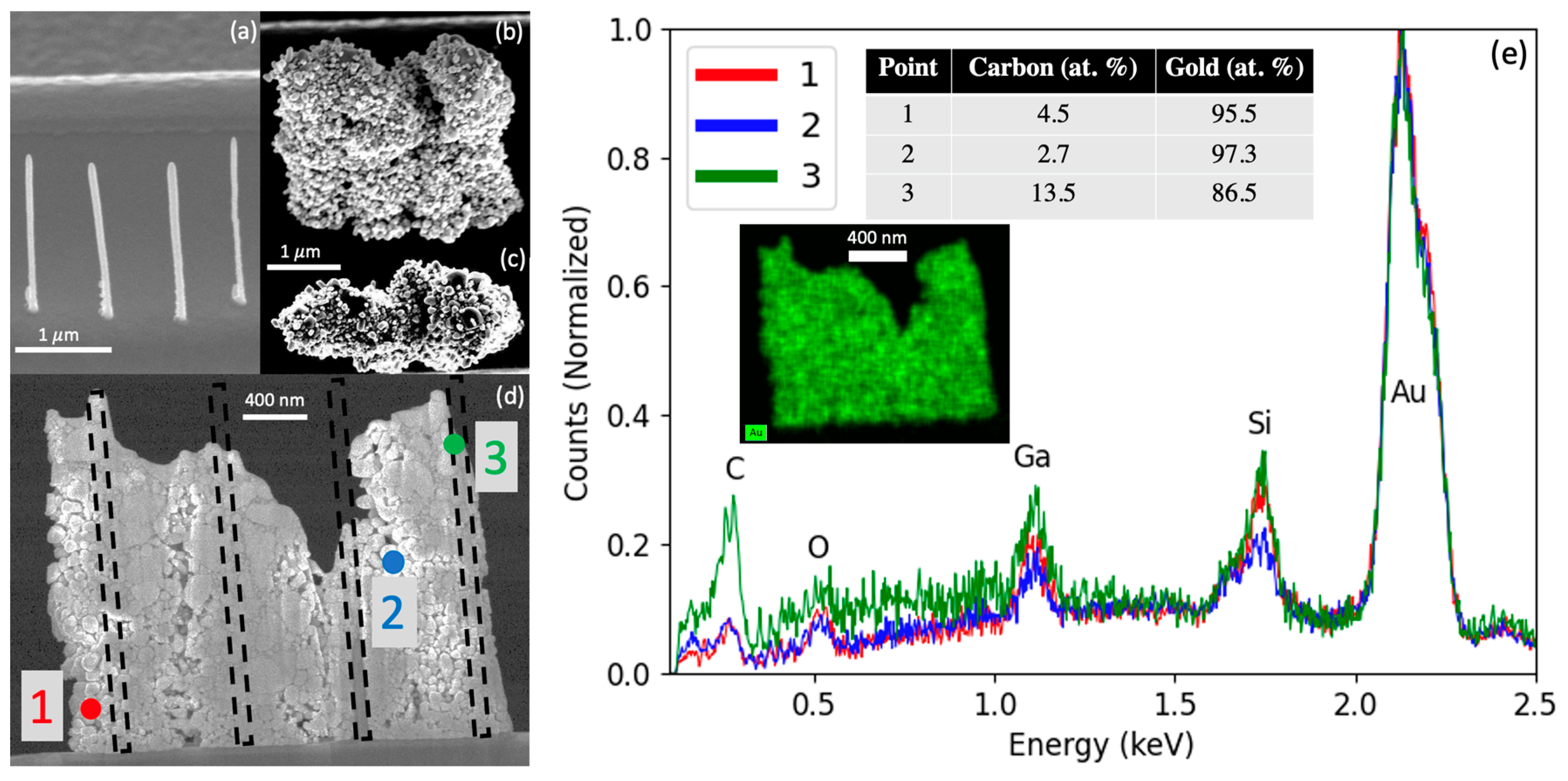
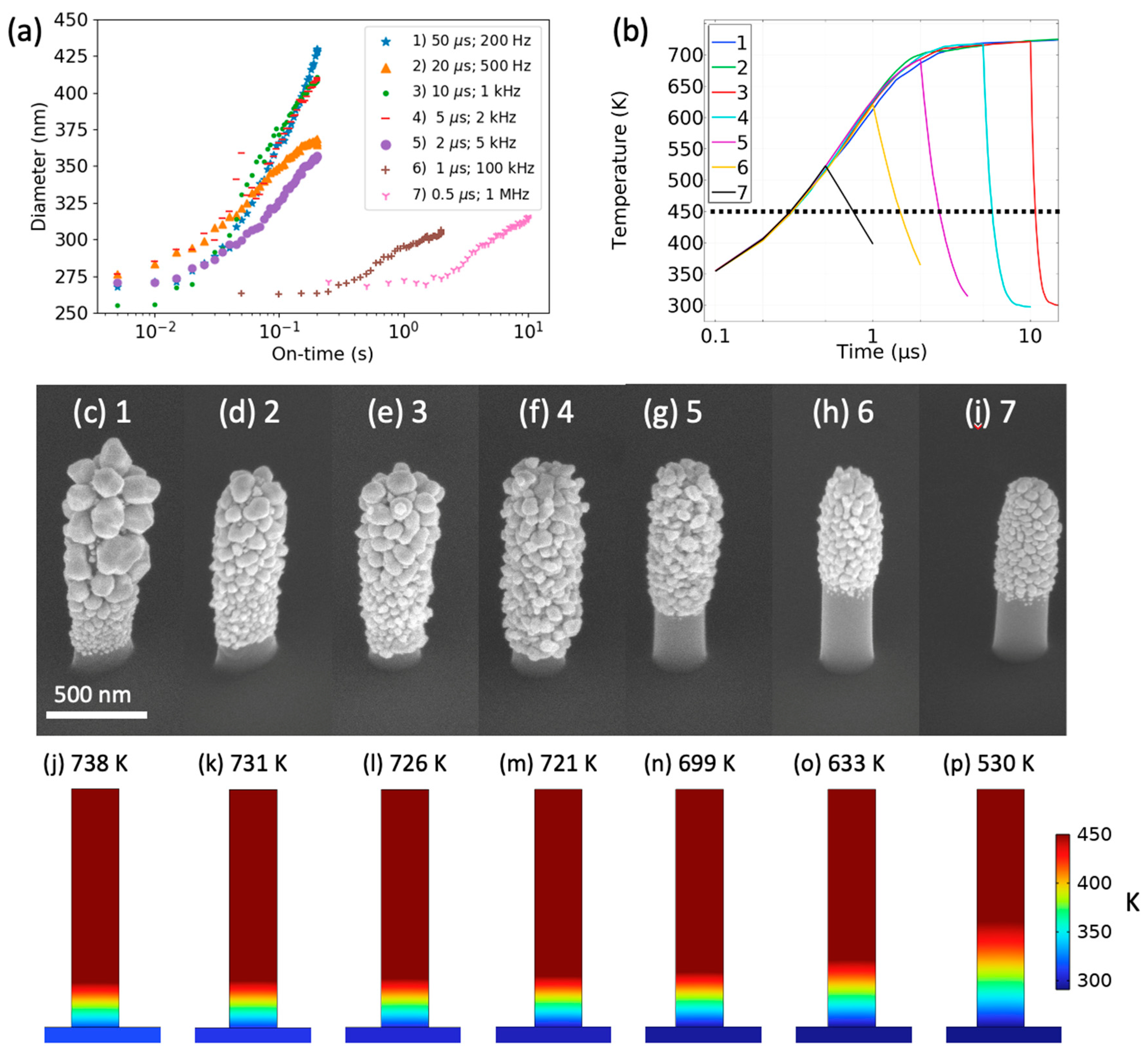
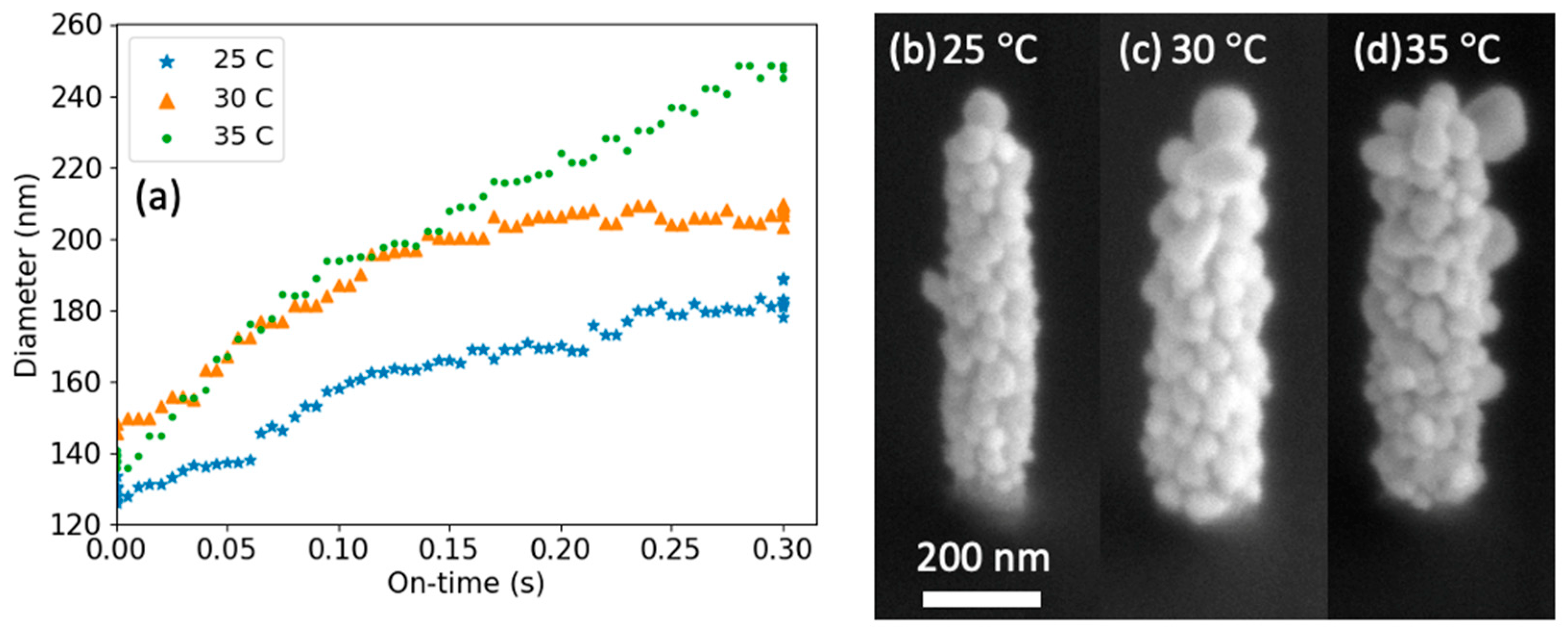
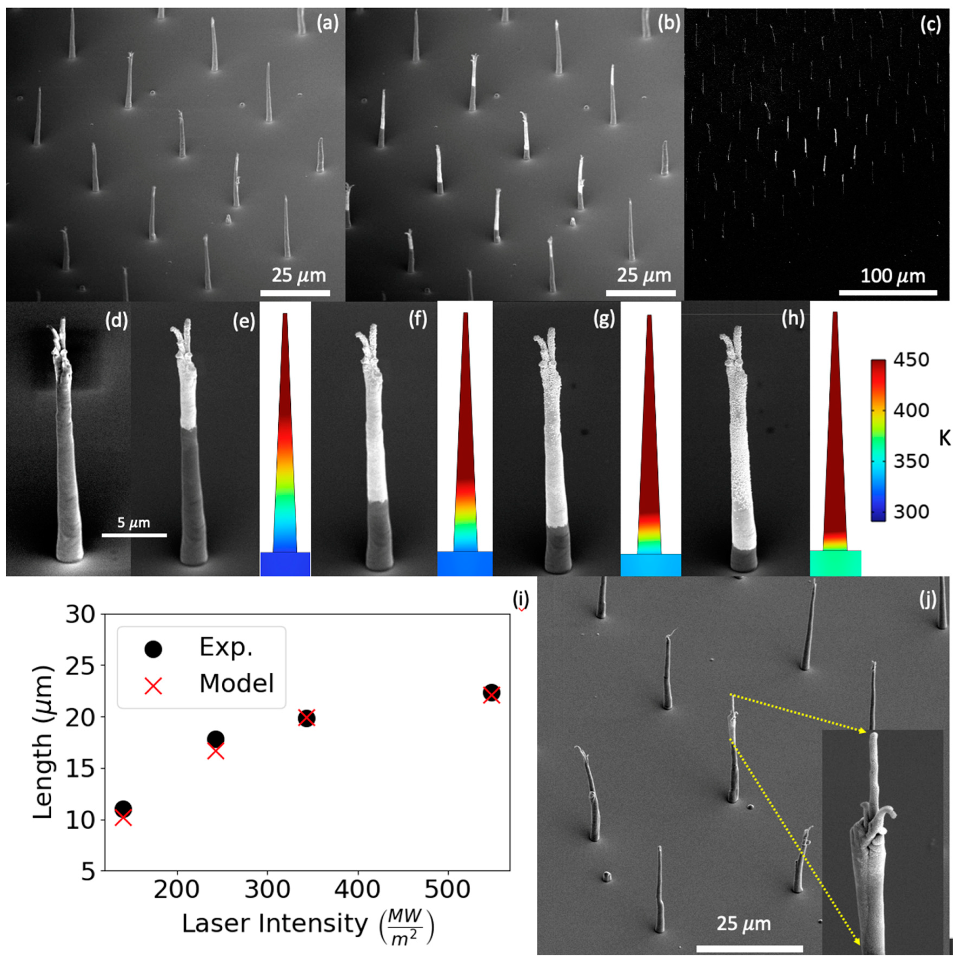
3. Results and Discussions
4. Conclusions
Supplementary Materials
Author Contributions
Funding
Data Availability Statement
Acknowledgments
Conflicts of Interest
References
- Mulders, J.J.L. Practical Precursor Aspects for Electron Beam Induced Deposition. Nanofabrication 2014, 1, 74–79. [Google Scholar] [CrossRef]
- Barth, S.; Huth, M.; Jungwirth, F. Precursors for Direct-Write Nanofabrication with Electrons. J. Mater. Chem. C 2020, 8, 15884–15919. [Google Scholar] [CrossRef]
- Van Dorp, W.F.; Hagen, C.W. A Critical Literature Review of Focused Electron Beam Induced Deposition. J. Appl. Phys. 2008, 104, 081301. [Google Scholar] [CrossRef]
- Silvis-Cividjian, N.; Hagen, C.W. Electron-Beam–Induced Nanometer-Scale Deposition. In Advances in Imaging and Electron Physics; Elsevier: Amsterdam, The Netherlands, 2006; Volume 143, pp. 1–235. [Google Scholar] [CrossRef]
- Utke, I.; Swiderek, P.; Höflich, K.; Madajska, K.; Jurczyk, J.; Martinović, P.; Szymańska, I.B. Coordination and Organometallic Precursors of Group 10 and 11: Focused Electron Beam Induced Deposition of Metals and Insight Gained from Chemical Vapour Deposition, Atomic Layer Deposition, and Fundamental Surface and Gas Phase Studies. Coord. Chem. Rev. 2022, 458, 213851. [Google Scholar] [CrossRef]
- Carden, W.G.; Lu, H.; Spencer, J.A.; Fairbrother, D.H.; McElwee-White, L. Mechanism-Based Design of Precursors for Focused Electron Beam-Induced Deposition. MRS Commun. 2018, 8, 343–357. [Google Scholar] [CrossRef]
- Botman, A.; Mulders, J.J.L.; Weemaes, R.; Mentink, S. Purification of Platinum and Gold Structures after Electron-Beam-Induced Deposition. Nanotechnology 2006, 17, 3779–3785. [Google Scholar] [CrossRef]
- Belić, D.; Shawrav, M.M.; Gavagnin, M.; Stöger-Pollach, M.; Wanzenboeck, H.D.; Bertagnolli, E. Direct-Write Deposition and Focused-Electron-Beam-Induced Purification of Gold Nanostructures. ACS Appl. Mater. Interfaces 2015, 7, 2467–2479. [Google Scholar] [CrossRef]
- Botman, A.; Mulders, J.J.L.; Hagen, C.W. Creating Pure Nanostructures from Electron-Beam-Induced Deposition Using Purification Techniques: A Technology Perspective. Nanotechnology 2009, 20, 372001. [Google Scholar] [CrossRef]
- Lewis, B.B.; Stanford, M.G.; Fowlkes, J.D.; Lester, K.; Plank, H.; Rack, P.D. Electron-Stimulated Purification of Platinum Nanostructures Grown via Focused Electron Beam Induced Deposition. Beilstein J. Nanotechnol. 2015, 6, 907–918. [Google Scholar] [CrossRef]
- Mehendale, S.; Mulders, J.J.L.; Trompenaars, P.H.F. A New Sequential EBID Process for the Creation of Pure Pt Structures from MeCpPtMe3. Nanotechnology 2013, 24, 145303. [Google Scholar] [CrossRef]
- Botman, A.; Hesselberth, M.; Mulders, J.J.L. Improving the Conductivity of Platinum-Containing Nano-Structures Created by Electron-Beam-Induced Deposition. Microelectron. Eng. 2008, 85, 1139–1142. [Google Scholar] [CrossRef]
- Fang, J.-Y.; Qin, S.-Q.; Zhang, X.-A.; Liu, D.-Q.; Chang, S.-L. Annealing Effect of Platinum-Incorporated Nanowires Created by Focused Ion/Electron-Beam-Induced Deposition. Chin. Phys. B 2014, 23, 088111. [Google Scholar] [CrossRef]
- Roberts, N.A.; Fowlkes, J.D.; Magel, G.A.; Rack, P.D. Enhanced Material Purity and Resolution via Synchronized Laser Assisted Electron Beam Induced Deposition of Platinum. Nanoscale 2012, 5, 408–415. [Google Scholar] [CrossRef]
- Hirt, L.; Reiser, A.; Spolenak, R.; Zambelli, T. Additive Manufacturing of Metal Structures at the Micrometer Scale. Adv. Mater. 2017, 29, 1604211. [Google Scholar] [CrossRef]
- Mohr-Weidenfeller, L.; Häcker, A.-V.; Reinhardt, C.; Manske, E. Two-Photon Direct Laser Writing Beyond the Diffraction Limit Using the Nanopositioning and Nanomeasuring Machine. Nanomanuf. Metrol. 2021, 4, 149–155. [Google Scholar] [CrossRef]
- Winkler, R.; Fowlkes, J.D.; Rack, P.D.; Plank, H. 3D Nanoprinting via Focused Electron Beams. J. Appl. Phys. 2019, 125, 210901. [Google Scholar] [CrossRef]
- Lasseter, J.; Rack, P.D.; Randolph, S.J. Selected Area Deposition of PtCx Nanostructures: Implications for Functional Coatings of 3D Nanoarchitectures. ACS Appl. Nano Mater. 2022, 5, 10890–10899. [Google Scholar] [CrossRef]
- Faust, M.; Enders, M.; Bruns, M.; Bräse, S.; Gao, K.; Seipenbusch, M. Synthesis of Nanostructured Pt/Oxide Catalyst Particles by MOCVD Process at Ambient Pressure. Surf. Coat. Technol. 2013, 230, 284–289. [Google Scholar] [CrossRef]
- Keller, L.; Al Mamoori, M.K.I.; Pieper, J.; Gspan, C.; Stockem, I.; Schröder, C.; Barth, S.; Winkler, R.; Plank, H.; Pohlit, M.; et al. Direct-Write of Free-Form Building Blocks for Artificial Magnetic 3D Lattices. Sci. Rep. 2018, 8, 6160. [Google Scholar] [CrossRef]
- Fischer, P.; Sanz-Hernández, D.; Streubel, R.; Fernández-Pacheco, A. Launching a New Dimension with 3D Magnetic Nanostructures. APL Mater. 2020, 8, 010701. [Google Scholar] [CrossRef]
- Sanz-Hernández, D.; Hamans, R.F.; Osterrieth, J.; Liao, J.-W.; Skoric, L.; Fowlkes, J.D.; Rack, P.D.; Lippert, A.; Lee, S.F.; Lavrijsen, R.; et al. Fabrication of Scaffold-Based 3D Magnetic Nanowires for Domain Wall Applications. Nanomaterials 2018, 8, 483. [Google Scholar] [CrossRef] [PubMed]
- Arnold, G.; Winkler, R.; Stermitz, M.; Orthacker, A.; Noh, J.-H.; Fowlkes, J.D.; Kothleitner, G.; Huth, M.; Rack, P.D.; Plank, H. Tunable 3D Nanoresonators for Gas-Sensing Applications. Adv. Funct. Mater. 2018, 28, 1707387. [Google Scholar] [CrossRef]
- Höflich, K.; Feichtner, T.; Hansjürgen, E.; Haverkamp, C.; Kollmann, H.; Lienau, C.; Silies, M. Resonant Behavior of a Single Plasmonic Helix. Opt. OPTICA 2019, 6, 1098–1105. [Google Scholar] [CrossRef]
- Kosters, D.; de Hoogh, A.; Zeijlemaker, H.; Acar, H.; Rotenberg, N.; Kuipers, L. Core–Shell Plasmonic Nanohelices. ACS Photonics 2017, 4, 1858–1863. [Google Scholar] [CrossRef]
- Benedetti, A.; Alam, B.; Esposito, M.; Tasco, V.; Leahu, G.; Belardini, A.; Li Voti, R.; Passaseo, A.; Sibilia, C. Precise Detection of Circular Dichroism in a Cluster of Nano-Helices by Photoacoustic Measurements. Sci. Rep. 2017, 7, 5257. [Google Scholar] [CrossRef]
- Esposito, M.; Tasco, V.; Todisco, F.; Benedetti, A.; Sanvitto, D.; Passaseo, A. Three Dimensional Chiral Metamaterial Nanospirals in the Visible Range by Vertically Compensated Focused Ion Beam Induced-Deposition. Adv. Opt. Mater. 2014, 2, 154–161. [Google Scholar] [CrossRef]
- Esposito, M.; Tasco, V.; Cuscunà, M.; Todisco, F.; Benedetti, A.; Tarantini, I.; Giorgi, M.D.; Sanvitto, D.; Passaseo, A. Nanoscale 3D Chiral Plasmonic Helices with Circular Dichroism at Visible Frequencies. ACS Photonics 2015, 2, 105–114. [Google Scholar] [CrossRef]
- Esposito, M.; Tasco, V.; Todisco, F.; Benedetti, A.; Tarantini, I.; Cuscunà, M.; Dominici, L.; Giorgi, M.D.; Passaseo, A. Tailoring Chiro-Optical Effects by Helical Nanowire Arrangement. Nanoscale 2015, 7, 18081–18088. [Google Scholar] [CrossRef]
- Tasco, V.; Esposito, M.; Todisco, F.; Benedetti, A.; Cuscunà, M.; Sanvitto, D.; Passaseo, A. Three-Dimensional Nanohelices for Chiral Photonics. Appl. Phys. A 2016, 122, 280. [Google Scholar] [CrossRef]
- Esposito, M.; Tasco, V.; Todisco, F.; Cuscunà, M.; Benedetti, A.; Sanvitto, D.; Passaseo, A. Triple-Helical Nanowires by Tomographic Rotatory Growth for Chiral Photonics. Nat. Commun. 2015, 6, 6484. [Google Scholar] [CrossRef]
- Pakeltis, G.; Hu, Z.; Nixon, A.G.; Mutunga, E.; Anyanwu, C.P.; West, C.A.; Idrobo, J.C.; Plank, H.; Masiello, D.J.; Fowlkes, J.D.; et al. Focused Electron Beam Induced Deposition Synthesis of 3D Photonic and Magnetic Nanoresonators. ACS Appl. Nano Mater. 2019, 2, 8075–8082. [Google Scholar] [CrossRef]
- Anyanwu, C.P.; Pakeltis, G.; Rack, P.D.; Masiello, D.J. Nanoscale Characterization of Individual Three-Dimensional Split Ring Resonator Dimers and Trimers. ACS Appl. Opt. Mater. 2023. [Google Scholar] [CrossRef]
- Kuhness, D.; Gruber, A.; Winkler, R.; Sattelkow, J.; Fitzek, H.; Letofsky-Papst, I.; Kothleitner, G.; Plank, H. High-Fidelity 3D Nanoprinting of Plasmonic Gold Nanoantennas. ACS Appl. Mater. Interfaces 2021, 13, 1178–1191. [Google Scholar] [CrossRef] [PubMed]
- Winkler, R.; Schmidt, F.-P.; Haselmann, U.; Fowlkes, J.D.; Lewis, B.B.; Kothleitner, G.; Rack, P.D.; Plank, H. Direct-Write 3D Nanoprinting of Plasmonic Structures. ACS Appl. Mater. Interfaces 2017, 9, 8233–8240. [Google Scholar] [CrossRef] [PubMed]
- Seewald, L.M.; Sattelkow, J.; Brugger-Hatzl, M.; Kothleitner, G.; Frerichs, H.; Schwalb, C.; Hummel, S.; Plank, H. 3D Nanoprinting of All-Metal Nanoprobes for Electric AFM Modes. Nanomaterials 2022, 12, 4477. [Google Scholar] [CrossRef] [PubMed]
- Plank, H.; Winkler, R.; Schwalb, C.H.; Hütner, J.; Fowlkes, J.D.; Rack, P.D.; Utke, I.; Huth, M. Focused Electron Beam-Based 3D Nanoprinting for Scanning Probe Microscopy: A Review. Micromachines 2020, 11, 48. [Google Scholar] [CrossRef]
- Sattelkow, J.; Fröch, J.E.; Winkler, R.; Hummel, S.; Schwalb, C.; Plank, H. Three-Dimensional Nanothermistors for Thermal Probing. ACS Appl. Mater. Interfaces 2019, 11, 22655–22667. [Google Scholar] [CrossRef]
- Utke, I.; Michler, J.; Winkler, R.; Plank, H. Mechanical Properties of 3D Nanostructures Obtained by Focused Electron/Ion Beam-Induced Deposition: A Review. Micromachines 2020, 11, 397. [Google Scholar] [CrossRef]
- Lewis, B.B.; Mound, B.A.; Srijanto, B.; Fowlkes, J.D.; Pharr, G.M.; Rack, P.D. Growth and Nanomechanical Characterization of Nanoscale 3D Architectures Grown via Focused Electron Beam Induced Deposition. Nanoscale 2017, 9, 16349–16356. [Google Scholar] [CrossRef]
- Baum, T.H.; Jones, C.R. Laser Chemical Vapor Deposition of Gold. Appl. Phys. Lett. 1985, 47, 538–540. [Google Scholar] [CrossRef]
- Baum, T.H. Laser Chemical Vapor Deposition of Gold: The Effect of Organometallic Structure. J. Electrochem. Soc. 1987, 134, 2616. [Google Scholar] [CrossRef]
- Parkhomenko, R.G.; Trubin, S.V.; Turgambaeva, A.E.; Igumenov, I.K. Deposition of Pure Gold Thin Films from Organometallic Precursors. J. Cryst. Growth 2015, 414, 143–150. [Google Scholar] [CrossRef]
- Xie, H.; Li, Z.; Zhu, J.; Li, C. Atomic Layer Deposition of Gold Nanoparticles with Controlled Size and Distribution on Titania Support. ChemNanoMat 2022, 8, e202200116. [Google Scholar] [CrossRef]
- Melechko, A.V.; Desikan, R.; McKnight, T.E.; Klein, K.L.; Rack, P.D. Synthesis of Vertically Aligned Carbon Nanofibres for Interfacing with Live Systems. J. Phys. D Appl. Phys. 2009, 42, 193001. [Google Scholar] [CrossRef]
- Green, M.A.; Keevers, M.J. Optical Properties of Intrinsic Silicon at 300 K. Prog. Photovolt. Res. Appl. 1995, 3, 189–192. [Google Scholar] [CrossRef]
- Stanford, M.G.; Lewis, B.B.; Noh, J.H.; Fowlkes, J.D.; Roberts, N.A.; Plank, H.; Rack, P.D. Purification of Nanoscale Electron-Beam-Induced Platinum Deposits via a Pulsed Laser-Induced Oxidation Reaction. ACS Appl. Mater. Interfaces 2014, 6, 21256–21263. [Google Scholar] [CrossRef]
- Mutunga, E.; Winkler, R.; Sattelkow, J.; Rack, P.D.; Plank, H.; Fowlkes, J.D. Impact of Electron-Beam Heating during 3D Nanoprinting. ACS Nano 2019, 13, 5198–5213. [Google Scholar] [CrossRef]
- Ergun, S.; Yasinsky, J.B.; Townsend, J.R. Transverse and Longitudinal Optical Properties of Graphite. Carbon 1967, 5, 403–408. [Google Scholar] [CrossRef]
- Butland, A.T.D.; Maddison, R.J. The Specific Heat of Graphite: An Evaluation of Measurements. J. Nucl. Mater. 1973, 49, 45–56. [Google Scholar] [CrossRef]
- Chung, D.D.L. Review Graphite. J. Mater. Sci. 2002, 37, 1475–1489. [Google Scholar] [CrossRef]
- Ciambriello, L.; Cavaliere, E.; Gavioli, L. Influence of Roughness, Porosity and Grain Morphology on the Optical Properties of Ultrathin Ag Films. Appl. Surf. Sci. 2022, 576, 151885. [Google Scholar] [CrossRef]
- Klein, K.L.; Melechko, A.V.; McKnight, T.E.; Retterer, S.T.; Rack, P.D.; Fowlkes, J.D.; Joy, D.C.; Simpson, M.L. Surface Characterization and Functionalization of Carbon Nanofibers. J. Appl. Phys. 2008, 103, 061301. [Google Scholar] [CrossRef]
- Merkulov, V.I.; Hensley, D.K.; Melechko, A.V.; Guillorn, M.A.; Lowndes, D.H.; Simpson, M.L. Control Mechanisms for the Growth of Isolated Vertically Aligned Carbon Nanofibers. J. Phys. Chem. B 2002, 106, 10570–10577. [Google Scholar] [CrossRef]
- Melechko, A.V.; McKnight, T.E.; Hensley, D.K.; Guillorn, M.A.; Borisevich, A.Y.; Merkulov, V.I.; Lowndes, D.H.; Simpson, M.L. Large-Scale Synthesis of Arrays of High-Aspect-Ratio Rigid Vertically Aligned Carbon Nanofibres. Nanotechnology 2003, 14, 1029–1035. [Google Scholar] [CrossRef]
- Stanford, M.G.; Mahady, K.; Lewis, B.B.; Fowlkes, J.D.; Tan, S.; Livengood, R.; Magel, G.A.; Moore, T.M.; Rack, P.D. Laser-Assisted Focused He+ Ion Beam Induced Etching with and without XeF2 Gas Assist. ACS Appl. Mater. Interfaces 2016, 8, 29155–29162. [Google Scholar] [CrossRef] [PubMed]
- Singh, U.B.; Pannu, C.; Agarwal, D.C.; Ojha, S.; Khan, S.A.; Ghosh, S.; Avasthi, D.K. Large Electronic Sputtering Yield of Nanodimensional Au Thin Films: Dominant Role of Thermal Conductivity and Electron Phonon Coupling Factor. J. Appl. Phys. 2017, 121, 095308. [Google Scholar] [CrossRef]
- Werner, W.S.M.; Glantschnig, K.; Ambrosch-Draxl, C. Optical Constants and Inelastic Electron-Scattering Data for 17 Elemental Metals. J. Phys. Chem. Ref. Data 2009, 38, 1013–1092. [Google Scholar] [CrossRef]


| Figure | Precursor Temperature (°C) | Template Material | Template Precursor | Laser Wavelength (nm) | Laser on-Time (s) | |
|---|---|---|---|---|---|---|
| 1 | 30 | PtCx | MeCpPtIVMe3 | 140 | 915 | 0.2 |
| 2 | 30 | AuCx | Me2Au (acac) | 13.4–58.5 | 915 | 4.3 |
| 3 | 30 | PtCx | MeCpPtIVMe3 | 140–1164 | 915 | 5.5 |
| 4 | 30 | PtCx | MeCpPtIVMe3 | 127 | 915 | 0.2–10 |
| 5 | 25, 30, 35 | AuCx | Me2Au (acac) | 140 | 915 | 0.3 |
| 6 | 30 | CNF | C2H2 + NH3 | 598, 140–548 | 785, 915 | 0.3–1.2 |
| Parameter | Value |
|---|---|
| Laser | 785 nm (single mode, ), 915 nm (multi mode, ) |
| Laser Intensity | 13.4–1164 |
| Laser Pulse Width | 500 ns–50 |
| Laser Repetition Rate | 200 Hz–1 MHz |
| FEBID SEM Voltage | 5 kV |
| FEBID SEM Current | 98 pA |
| Typical SEM Base Pressure | 5 |
| SEM Room Temperature | 25 °C |
| Typical Precursor Temperature | 30 °C |
Disclaimer/Publisher’s Note: The statements, opinions and data contained in all publications are solely those of the individual author(s) and contributor(s) and not of MDPI and/or the editor(s). MDPI and/or the editor(s) disclaim responsibility for any injury to people or property resulting from any ideas, methods, instructions or products referred to in the content. |
© 2023 by the authors. Licensee MDPI, Basel, Switzerland. This article is an open access article distributed under the terms and conditions of the Creative Commons Attribution (CC BY) license (https://creativecommons.org/licenses/by/4.0/).
Share and Cite
Lasseter, J.; Rack, P.D.; Randolph, S.J. Selected Area Deposition of High Purity Gold for Functional 3D Architectures. Nanomaterials 2023, 13, 757. https://doi.org/10.3390/nano13040757
Lasseter J, Rack PD, Randolph SJ. Selected Area Deposition of High Purity Gold for Functional 3D Architectures. Nanomaterials. 2023; 13(4):757. https://doi.org/10.3390/nano13040757
Chicago/Turabian StyleLasseter, John, Philip D. Rack, and Steven J. Randolph. 2023. "Selected Area Deposition of High Purity Gold for Functional 3D Architectures" Nanomaterials 13, no. 4: 757. https://doi.org/10.3390/nano13040757
APA StyleLasseter, J., Rack, P. D., & Randolph, S. J. (2023). Selected Area Deposition of High Purity Gold for Functional 3D Architectures. Nanomaterials, 13(4), 757. https://doi.org/10.3390/nano13040757