

Integrated Optical Filters with Hyperbolic Metamaterials

 , , , , , , and
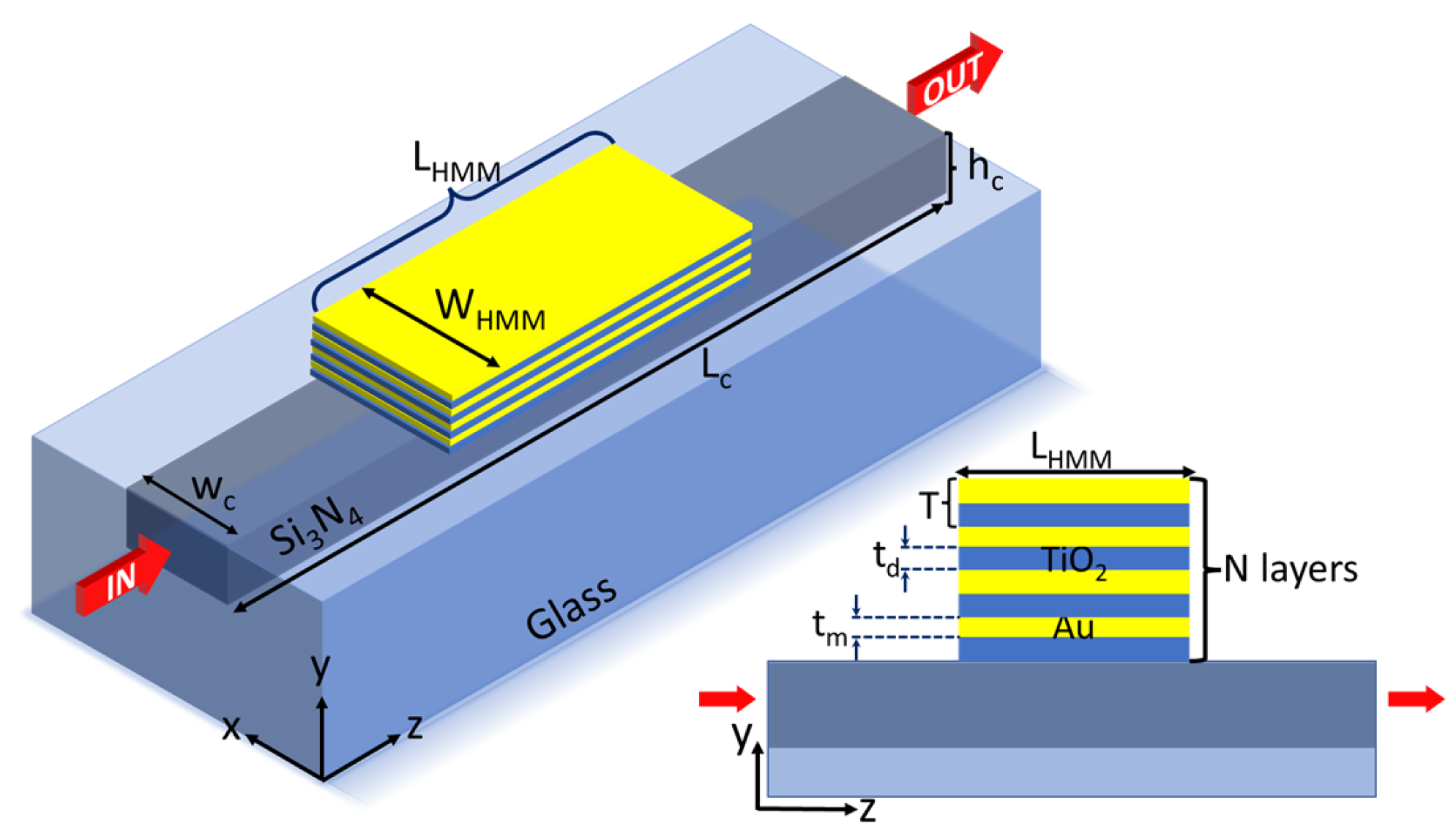
Abstract
1. Introduction
2. Materials and Methods
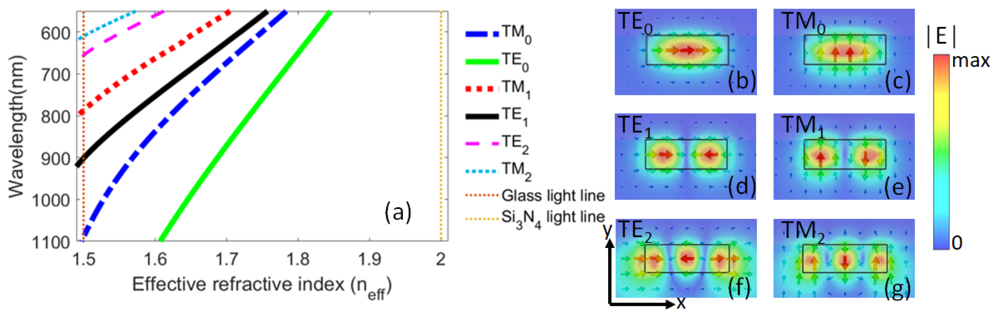
2.1. Description of the Integrated System
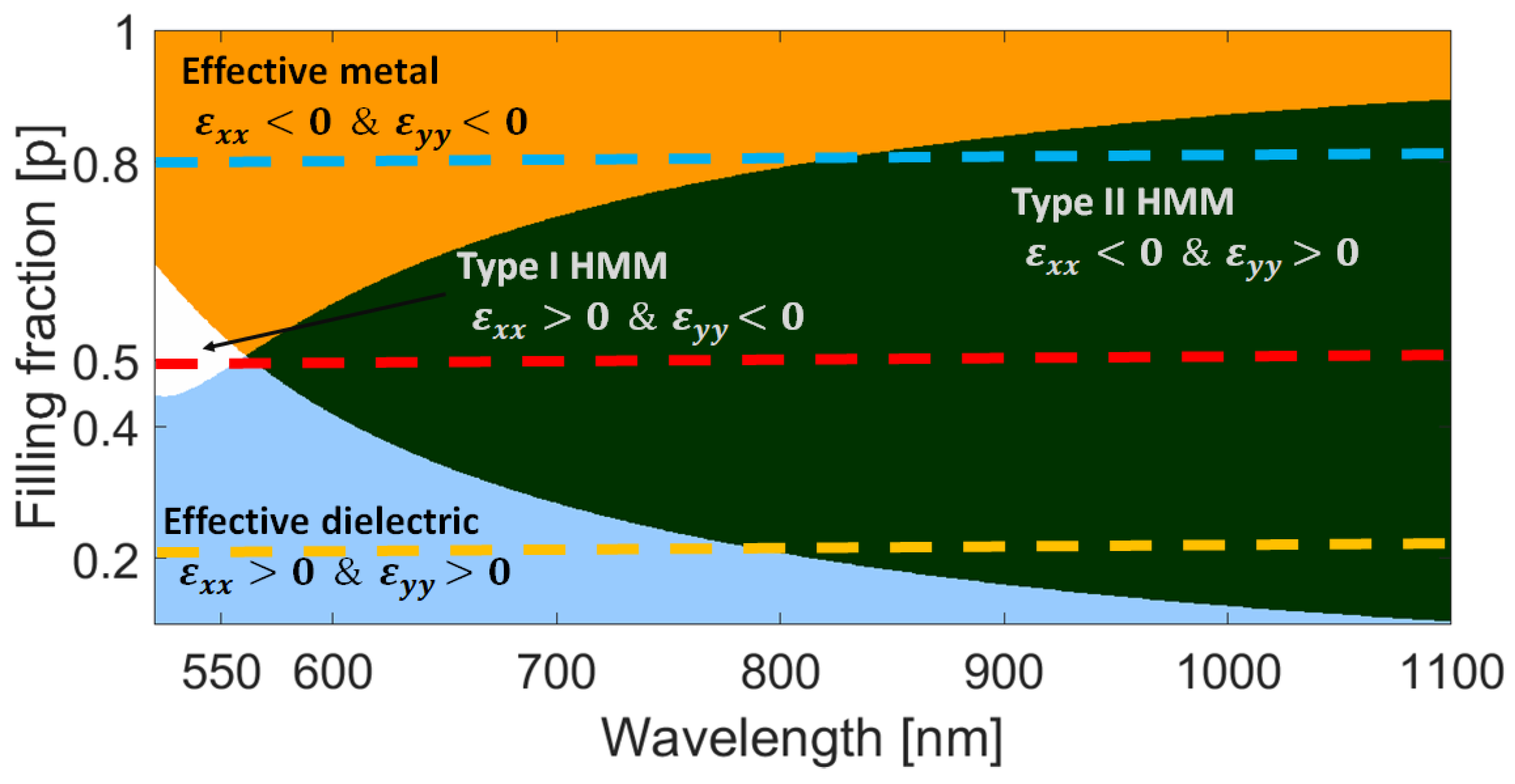
2.2. Effective Medium Theory
2.3. Transfer Matrix Method
2.4. Light Propagation in a 3D Integrated Device
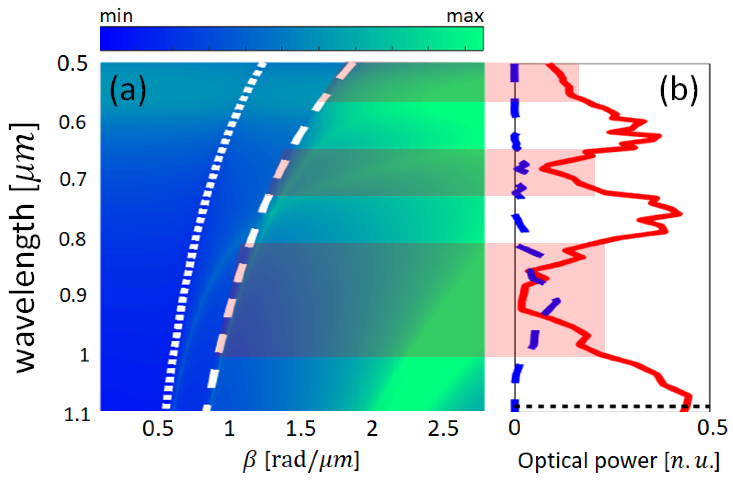
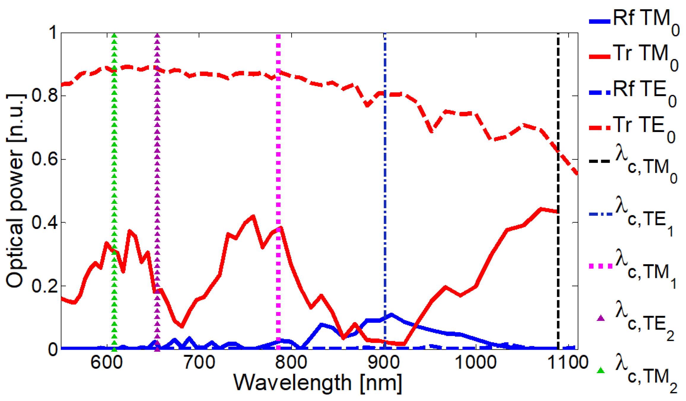
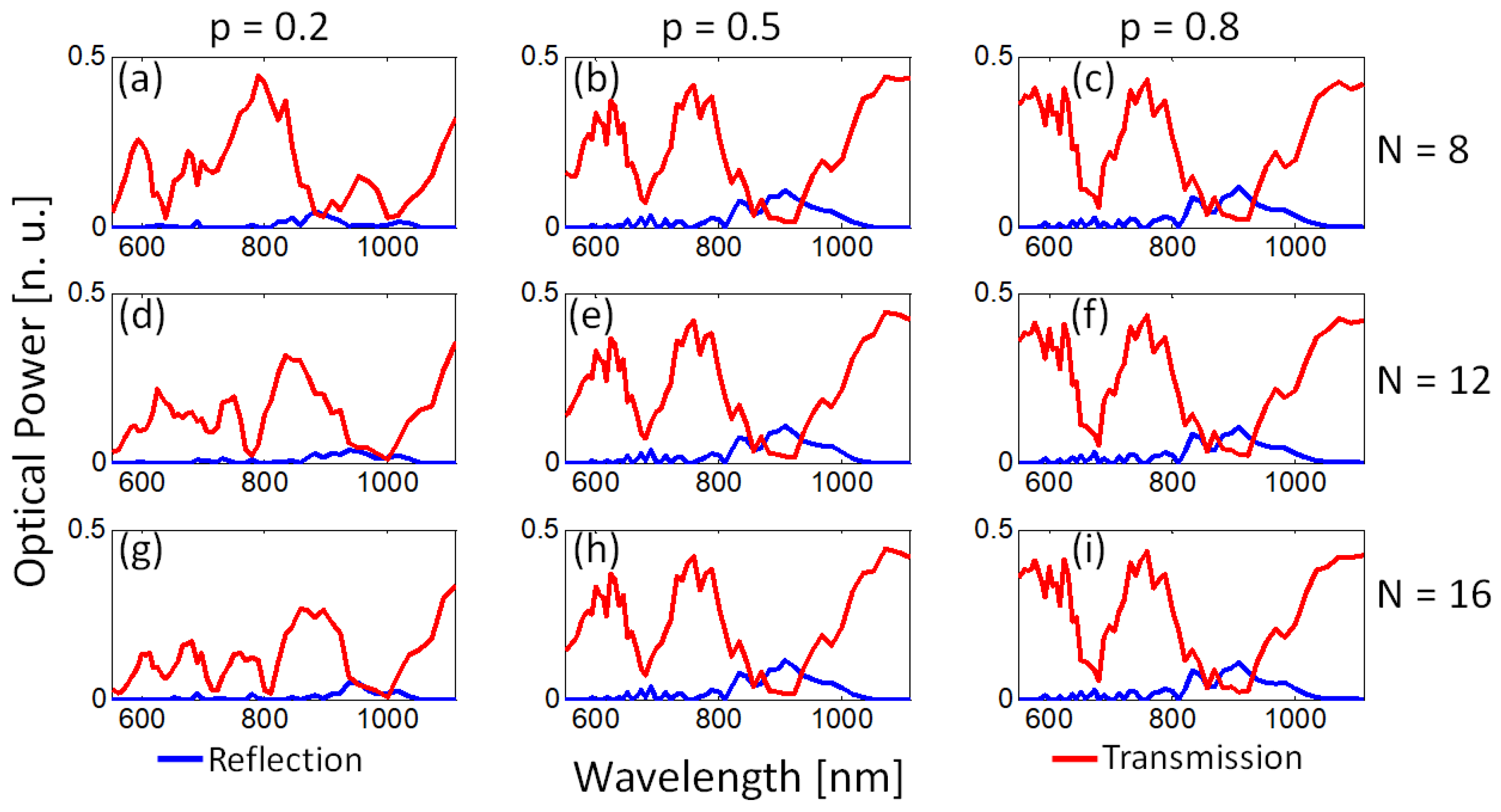
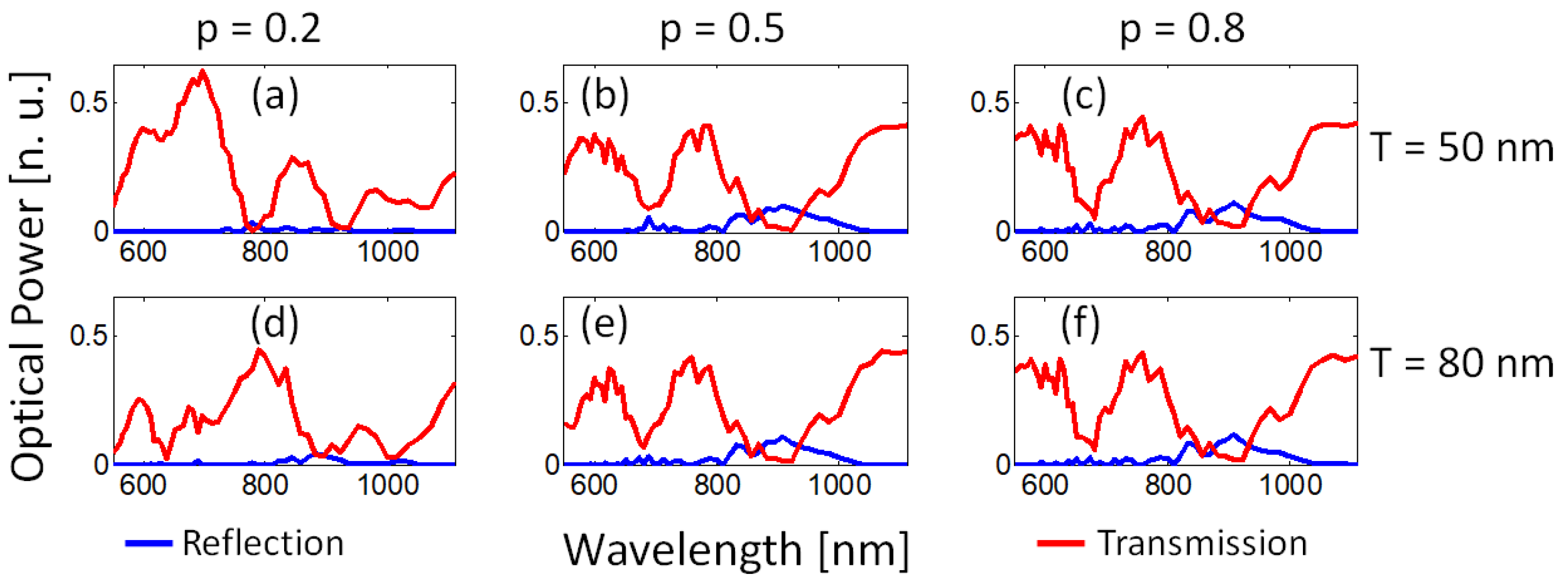
3. Results
4. Discussion
Author Contributions
Funding
Institutional Review Board Statement
Informed Consent Statement
Data Availability Statement
Acknowledgments
Conflicts of Interest
Abbreviations
| TM | Transverse Magnetic |
| TE | Transverse Electric |
| Wavelength spectral bandwidth | |
| FWHM | Full width at half maximum |
References
- Kogelnik, H. An Introduction to Integrated Optics. IEEE Trans. Microw. Theory Tech. 1975, 23, 2–16. [Google Scholar] [CrossRef]
- Suhara, T.; Nishihara, H. Integrated optics components and devices using periodic structures. IEEE J. Quantum Electron. 1986, 22, 845–867. [Google Scholar] [CrossRef]
- Okamoto, K. Recent progress of integrated optics planar lightwave circuits. Opt. Quantum Electron. 1999, 31, 107–129. [Google Scholar] [CrossRef]
- Ma, H.; Jen, A.Y.; Dalton, L. Polymer-Based Optical Waveguides: Materials, Processing, and Devices. Adv. Mater. 2002, 14, 1339–1365. [Google Scholar] [CrossRef]
- Broquin, J.E. Glass integrated optics: State of the art and position toward other technologies. In Proceedings of the Integrated Optics: Devices, Materials, and Technologies XI, San Jose, CA, USA, 20–25 January 2007; Sidorin, Y., Waechter, C.A., Eds.; International Society for Optics and Photonics, SPIE: Bellingham, WA, USA, 2007; Volume 6475, p. 647507. [Google Scholar] [CrossRef]
- Sohler, W.; Hu, H.; Ricken, R.; Quiring, V.; Vannahme, C.; Herrmann, H.; Büchter, D.; Reza, S.; Grundkötter, W.; Orlov, S.; et al. Integrated Optical Devices in Lithium Niobate. Opt. Photon. News 2008, 19, 24–31. [Google Scholar] [CrossRef]
- Tong, X.C. Advanced Materials for Integrated Optical Waveguides; Springer: Cham, Switzerland, 2013; p. 552. [Google Scholar]
- Zheludev, N.I.; Kivshar, Y.S. From metamaterials to metadevices. Nat. Mater. 2012, 19, 917–924. [Google Scholar] [CrossRef]
- Urbas, A.M.; Jacob, Z.; Negro, L.D.; Engheta, N.; Boardman, A.D.; Egan, P.; Khanikaev, A.B.; Menon, V.; Ferrera, M.; Kinsey, N.; et al. Roadmap on optical metamaterials. J. Opt. 2016, 18, 093005. [Google Scholar] [CrossRef]
- Liang, Y.; Koshelev, K.; Zhang, F.; Lin, H.; Lin, S.; Wu, J.; Jia, B.; Kivshar, Y. Bound States in the Continuum in Anisotropic Plasmonic Metasurfaces. Nano Lett. 2020, 20, 6351–6356. [Google Scholar] [CrossRef]
- Rabus, D.G.; Sada, C. Integrated Ring Resonators, 2nd ed.; Springer: Cham, Switzerland, 2020; p. 360. [Google Scholar]
- Holmgaard, T.; Chen, Z.; Bozhevolnyi, S.I.; Markey, L.; Dereux, A. Dielectric-loaded plasmonic waveguide-ring resonators. Opt. Express 2009, 17, 2968–2975. [Google Scholar] [CrossRef]
- Pérez-Galacho, D.; Alonso-Ramos, C.; Mazeas, F.; Roux, X.L.; Oser, D.; Zhang, W.; Marris-Morini, D.; Labonté, L.; Tanzilli, S.; Cassan, É.; et al. Optical pump-rejection filter based on silicon sub-wavelength engineered photonic structures. Opt. Lett. 2017, 42, 1468–1471. [Google Scholar] [CrossRef]
- Čtyroký, J.; Wangüemert-Pérez, J.G.; Kwiecien, P.; Richter, I.; Litvik, J.; Schmid, J.H.; Íñigo Molina-Fernández, I.; Moñux, A.O.M.; Dado, M.; Cheben, P. Design of narrowband Bragg spectral filters in subwavelength grating metamaterial waveguides. Opt. Express 2018, 26, 179–194. [Google Scholar] [CrossRef]
- Quaranta, G.; Basset, G.; Martin, O.J.F.; Gallinet, B. Recent Advances in Resonant Waveguide Gratings. Laser Photonics Rev. 2018, 12, 1800017. [Google Scholar] [CrossRef]
- Matsko, A.; Ilchenko, V. Optical resonators with whispering-gallery modes-part I: Basics. IEEE J. Sel. Top. Quantum Electron. 2006, 12, 3–14. [Google Scholar] [CrossRef]
- Lu, H.; Liu, X.; Mao, D.; Wang, L.; Gong, Y. Tunable band-pass plasmonic waveguide filters with nanodisk resonators. Opt. Express 2010, 18, 17922–17927. [Google Scholar] [CrossRef]
- Khani, S.; Danaie, M.; Rezaei, P. Realization of single-mode plasmonic bandpass filters using improved nanodisk resonators. Opt. Commun. 2018, 420, 147–156. [Google Scholar] [CrossRef]
- Tao, J.; Huang, X.G.; Lin, X.; Zhang, Q.; Jin, X. A narrow-band subwavelength plasmonic waveguide filter with asymmetrical multiple-teeth-shaped structure. Opt. Express 2009, 17, 13989–13994. [Google Scholar] [CrossRef]
- López-Rayón, F.; Arroyo Carrasco, M.L.; Rodríguez-Beltrán, R.I.; Salas-Montiel, R.; Téllez-Limón, R. Plasmonic-Induced Transparencies in an Integrated Metaphotonic System. Nanomaterials 2022, 12, 1701. [Google Scholar] [CrossRef]
- Lin, X.S.; Huang, X.G. Tooth-shaped plasmonic waveguide filters with nanometeric sizes. Opt. Lett. 2008, 33, 2874–2876. [Google Scholar] [CrossRef]
- Neutens, P.; Lagae, L.; Borghs, G.; Dorpe, P.V. Plasmon filters and resonators in metal-insulator-metal waveguides. Opt. Express 2012, 20, 3408–3423. [Google Scholar] [CrossRef]
- Tan, D.T.H.; Ikeda, K.; Fainman, Y. Cladding-modulated Bragg gratings in silicon waveguides. Opt. Lett. 2009, 34, 1357–1359. [Google Scholar] [CrossRef]
- Yun, H.; Hammood, M.; Chrostowski, L.; Jaeger, N.A.F. Optical Add-drop Filters using Cladding-modulated Sub-wavelength Grating Contra-directional Couplers for Silicon-on-Insulator Platforms. In Proceedings of the 2019 IEEE 10th Annual Information Technology, Electronics and Mobile Communication Conference (IEMCON), Vancouver, BC, Canada, 17–19 October 2019; pp. 0926–0931. [Google Scholar] [CrossRef]
- Yen, T.H.; Shih, B.H.; Cheng, N.W.; Hung, Y.J. Linewidth-adjustable bandpass filter based on silicon cladding-modulated waveguide moiré Bragg gratings. In Proceedings of the Conference on Lasers and Electro-Optics, San Jose, CA, USA, 13–18 May 2018; p. JW2A.38. [Google Scholar] [CrossRef]
- Yen, T.H.; Wu, C.J.; Yu, C.J.; Hung, Y.J. Silicon photonics multi-channel Bragg reflectors based on narrowband cladding-modulated gratings. In Proceedings of the 2017 Conference on Lasers and Electro-Optics (CLEO), San Jose, CA, USA, 14–19 May 2017; pp. 1–2. [Google Scholar]
- Jin, Y.; Fernez, N.; Pennec, Y.; Bonello, B.; Moiseyenko, R.P.; Hémon, S.; Pan, Y.; Djafari-Rouhani, B. Tunable waveguide and cavity in a phononic crystal plate by controlling whispering-gallery modes in hollow pillars. Phys. Rev. B 2016, 93, 054109. [Google Scholar] [CrossRef]
- Mendez-Astudillo, M.; Okayama, H.; Nakajima, H. Silicon optical filter with transmission peaks in wide stopband obtained by anti-symmetric photonic crystal with defect in multimode waveguides. Opt. Express 2018, 26, 1841–1850. [Google Scholar] [CrossRef] [PubMed]
- Tellez-Limon, R.; Blaize, S.; Gardillou, F.; Coello, V.; Salas-Montiel, R. Excitation of surface plasmon polaritons in a gold nanoslab on ion-exchanged waveguide technology. Appl. Opt. 2020, 59, 572–578. [Google Scholar] [CrossRef] [PubMed]
- Poddubny, A.; Iorsh, I.; Belov, P.; Kivshar, Y. Hyperbolic metamaterials. Nat. Photonics 2013, 7, 948–957. [Google Scholar] [CrossRef]
- Shekhar, P.; Atkinson, J.; Jacob, Z. Hyperbolic metamaterials: Fundamentals and applications. Nano Converg. 2014, 1, 1–14. [Google Scholar] [CrossRef]
- Ferrari, L.; Wu, C.; Lepage, D.; Zhang, X.; Liu, Z. Hyperbolic metamaterials and their applications. Prog. Quantum Electron. 2015, 40, 1–40. [Google Scholar] [CrossRef]
- Dudek, M.; Kowerdziej, R.; Pianelli, A.; Parka, J. Graphene-based tunable hyperbolic microcavity. Sci. Rep. 2021, 11, 74. [Google Scholar] [CrossRef]
- Pianelli, A.; Caligiuri, V.; Dudek, M.; Kowerdziej, R.; Chodorow, U.; Sielezin, K.; De Luca, A.; Caputo, R.; Parka, J. Active control of dielectric singularities in indium-tin-oxides hyperbolic metamaterials. Sci. Rep. 2022, 12, 16961. [Google Scholar] [CrossRef]
- Rytov, S. Electromagnetic properties of a finely stratified medium. Sov. Phys. Jept 1956, 2, 466–475. [Google Scholar]
- Drachev, V.P.; Podolskiy, V.A.; Kildishev, A.V. Hyperbolic metamaterials: New physics behind a classical problem. Opt. Express 2013, 21, 15048–15064. [Google Scholar] [CrossRef]
- Kidwai, O.; Zhukovsky, S.V.; Sipe, J.E. Effective-medium approach to planar multilayer hyperbolic metamaterials: Strengths and limitations. Phys. Rev. A 2012, 85, 053842. [Google Scholar] [CrossRef]
- Tumkur, T.; Barnakov, Y.; Kee, S.T.; Noginov, M.A.; Liberman, V. Permittivity evaluation of multilayered hyperbolic metamaterials: Ellipsometry vs. reflectometry. J. Appl. Phys. 2015, 117, 103104. [Google Scholar] [CrossRef]
- Hu, S.; Du, S.; Li, J.; Gu, C. Multidimensional Image and Beam Splitter Based on Hyperbolic Metamaterials. Nano Lett. 2021, 21, 1792–1799. [Google Scholar] [CrossRef] [PubMed]
- Zhukovsky, S.V.; Orlov, A.A.; Babicheva, V.E.; Lavrinenko, A.V.; Sipe, J.E. Photonic-band-gap engineering for volume plasmon polaritons in multiscale multilayer hyperbolic metamaterials. Phys. Rev. A 2014, 90, 013801. [Google Scholar] [CrossRef]
- Kalusniak, S.; Orphal, L.; Sadofev, S. Demonstration of hyperbolic metamaterials at telecommunication wavelength using Ga-doped ZnO. Opt. Express 2015, 23, 32555–32560. [Google Scholar] [CrossRef] [PubMed]
- Rizza, C.; Ciattoni, A.; Spinozzi, E.; Columbo, L. Terahertz active spatial filtering through optically tunable hyperbolic metamaterials. Opt. Lett. 2012, 37, 3345–3347. [Google Scholar] [CrossRef]
- Naik, G.V.; Liu, J.; Kildishev, A.V.; Shalaev, V.M.; Boltasseva, A. Demonstration of Al:ZnO as a plasmonic component for near-infrared metamaterials. Proc. Natl. Acad. Sci. USA 2012, 109, 8834–8838. [Google Scholar] [CrossRef]
- Zhou, X.; Yin, X.; Zhang, T.; Chen, L.; Li, X. Ultrabroad terahertz bandpass filter by hyperbolic metamaterial waveguide. Opt. Express 2015, 23, 11657–11664. [Google Scholar] [CrossRef]
- Hemmer, E.; Benayas, A.; Légaré, F.; Vetrone, F. Exploiting the biological windows: Current perspectives on fluorescent bioprobes emitting above 1000 nm. Nanoscale Horizons 2016, 13, 168–184. [Google Scholar] [CrossRef]
- Vial, A.; Grimault, A.S.; Macías, D.; Barchiesi, D.; de la Chapelle, M.L. Improved analytical fit of gold dispersion: Application to the modeling of extinction spectra with a finite-difference time-domain method. Phys. Rev. B 2005, 71, 085416. [Google Scholar] [CrossRef]
- Barchiesi, D.; Grosges, T. Fitting the optical constants of gold, silver, chromium, titanium, and aluminum in the visible bandwidth. J. Nanophotonics 2014, 8, 083097, Errata in J. Nanophotonics 2015, 8, 089996. [Google Scholar] [CrossRef]
- DeVore, J.R. Refractive Indices of Rutile and Sphalerite. J. Opt. Soc. Am. 1951, 41, 416–419. [Google Scholar] [CrossRef]
- Téllez-Limón, R.; Salas-Montiel, R. Nanowires Integrated to Optical Waveguides. In Nanowires; Peng, X., Ed.; IntechOpen: Rijeka, Croatia, 2021; Chapter 8. [Google Scholar] [CrossRef]
- Wittig, T.; Schuhmann, R.; Weiland, T. Model order reduction for large systems in computational electromagnetics. Linear Algebra Appl. 2006, 415, 499–530. [Google Scholar] [CrossRef]


Disclaimer/Publisher’s Note: The statements, opinions and data contained in all publications are solely those of the individual author(s) and contributor(s) and not of MDPI and/or the editor(s). MDPI and/or the editor(s) disclaim responsibility for any injury to people or property resulting from any ideas, methods, instructions or products referred to in the content. |
© 2023 by the authors. Licensee MDPI, Basel, Switzerland. This article is an open access article distributed under the terms and conditions of the Creative Commons Attribution (CC BY) license (https://creativecommons.org/licenses/by/4.0/).
Share and Cite
Abdulkareem, M.-u.A.; López-Rayón, F.; Sosa-Sánchez, C.T.; Bautista González, R.E.; Arroyo Carrasco, M.L.; Peña-Gomar, M.; Coello, V.; Téllez-Limón, R. Integrated Optical Filters with Hyperbolic Metamaterials. Nanomaterials 2023, 13, 759. https://doi.org/10.3390/nano13040759
Abdulkareem M-uA, López-Rayón F, Sosa-Sánchez CT, Bautista González RE, Arroyo Carrasco ML, Peña-Gomar M, Coello V, Téllez-Limón R. Integrated Optical Filters with Hyperbolic Metamaterials. Nanomaterials. 2023; 13(4):759. https://doi.org/10.3390/nano13040759
Chicago/Turabian StyleAbdulkareem, Mas-ud A., Fernando López-Rayón, Citlalli T. Sosa-Sánchez, Ramsés E. Bautista González, Maximino L. Arroyo Carrasco, Marycarmen Peña-Gomar, Victor Coello, and Ricardo Téllez-Limón. 2023. "Integrated Optical Filters with Hyperbolic Metamaterials" Nanomaterials 13, no. 4: 759. https://doi.org/10.3390/nano13040759
APA StyleAbdulkareem, M.-u. A., López-Rayón, F., Sosa-Sánchez, C. T., Bautista González, R. E., Arroyo Carrasco, M. L., Peña-Gomar, M., Coello, V., & Téllez-Limón, R. (2023). Integrated Optical Filters with Hyperbolic Metamaterials. Nanomaterials, 13(4), 759. https://doi.org/10.3390/nano13040759