Article

Effects of Charge Trapping on Memory Characteristics for HfO2-Based Ferroelectric Field Effect Transistors

1
Institute of Microelectronics, Chinese Academy of Sciences, Beijing 100029, China
2
School of Microelectronics, University of Chinese Academy of Sciences, Beijing 100049, China
3
School of Electronic Science, Xi’an Jiaotong University, Xi’an 710049, China
4
Beijing Zhongke New Micro Technology Department Co., Ltd., Beijing 100029, China
5
Department of Microelectronics, Belarusian State University of Informatics and Radioelectronics, 220015 Minsk, Belarus
*
Authors to whom correspondence should be addressed.
Nanomaterials 2023, 13(4), 638; https://doi.org/10.3390/nano13040638
Submission received: 31 December 2022 / Revised: 24 January 2023 / Accepted: 30 January 2023 / Published: 6 February 2023

Abstract

:
A full understanding of the impact of charge trapping on the memory window (MW) of HfO2-based ferroelectric field effect transistors (FeFETs) will permit the design of program and erase protocols, which will guide the application of these devices and maximize their useful life. The effects of charge trapping have been studied by changing the parameters of the applied program and erase pulses in a test sequence. With increasing the pulse amplitude and pulse width, the MW increases first and then decreases, a result attributed to the competition between charge trapping (CT) and ferroelectric switching (FS). This interaction between CT and FS is analyzed in detail using a single-pulse technique. In addition, the experimental data show that the conductance modulation characteristics are affected by the CT in the analog synaptic behavior of the FeFET. Finally, a theoretical investigation is performed in Sentaurus TCAD, providing a plausible explanation of the CT effect on the memory characteristics of the FeFET. This work is helpful to the study of the endurance fatigue process caused by the CT effect and to optimizing the analog synaptic behavior of the FeFET.

1. Introduction

Ferroelectric field effect transistors (FeFETs) have become one of the most promising candidate devices for emerging nonvolatile memory applications due to the discovery of the ferroelectricity in HfO2 thin films [1,2,3]. HfO2-based FeFETs have the advantages of excellent compatibility with CMOS (Complementary Metal Oxide Semiconductor) processes, high scalability, and mature manufacturability, which are lacking with traditional perovskite ferroelectric materials [4,5,6]. Significant progress has been made in promoting the development of the advanced technology, improving device performance, and exploring novel device applications for these HfO2-based FeFETs [7,8,9,10]. For example, they were integrated into technology nodes below 28 nm by fabricating FeFETs in non-planar configurations [11]; the performance of the FeFETs device was optimized by changing the device structure [12,13], and basic logic operation was realized [14]. These devices are also increasingly drawing the attention of the emerging neuromorphic and analog-in-memory computing sectors, showing the great prospects for applications of this ferroelectric technology [15].
However, charge trapping (CT) in HfO2-based FeFETs is a major challenge, as it limits their full application. HfO2 is a dielectric material with high density intrinsic defects. The HfO2/interlayer and interlayer/semiconductor interfaces of HfO2-based FeFETs typically have defects, which will trap electrons and holes [16,17,18]. The threshold voltage (VT) shift caused by CT is opposite to the VT shift caused by ferroelectric switching (FS), so that the memory window (MW) of the device is reduced. With an increase in the number of cycles, the newly generated defects caused by the cycles capture more charges until the MW disappears [15]; the endurance of the conventional HfO2-based FeFET is limited to 104–105 program (PGM) and erase (ERS) cycles, which greatly limits the application of the FeFET in many fields [19,20]. Therefore, understanding the interaction between CT and FS is essential for the optimization of FeFETs. Currently, some progress has been made in the study of the CT effect in FeFET devices [21,22,23], but no convincing conclusion has been reached.
This work uses an FeFET based on Hf0.5Zr0.5O2 (HZO), and systematically studies the CT effect in a fabricated W/TiN/HZO/SiO2/Si gate stacked FeFET by applying pulse sequences with various controlled pulse amplitudes and widths to the gate of the device, and with various read delay times. The competition between CT and FS is analyzed by a single-pulse technique. The pulse width and pulse amplitude testing schemes are used to study the influence of the CT effect on the conductance modulation characteristics of the FeFET. Finally, the mechanism of the CT effect on the MW of the FeFET is analyzed using the Sentaurus TCAD tool.
The rest of this paper is arranged as follows. Section 2 demonstrates the fabrication and testing methods of the FeFET; Section 3 introduces the effects of program/erase pulse amplitude, pulse width and read delay time on the MW of the FeFET, the competitive relationship between the CT and FS, the influence of the CT effect on the conductance modulation characteristics, and the P-V characteristics are tested to verify the ferroelectric performance of FeFET, and the endurance is also tested to confirm the influence of CT effect on FeFET; in Section 4, the mechanism of the CT effect on the MW is analyzed by using TCAD tool. Section 5 provides the conclusion.

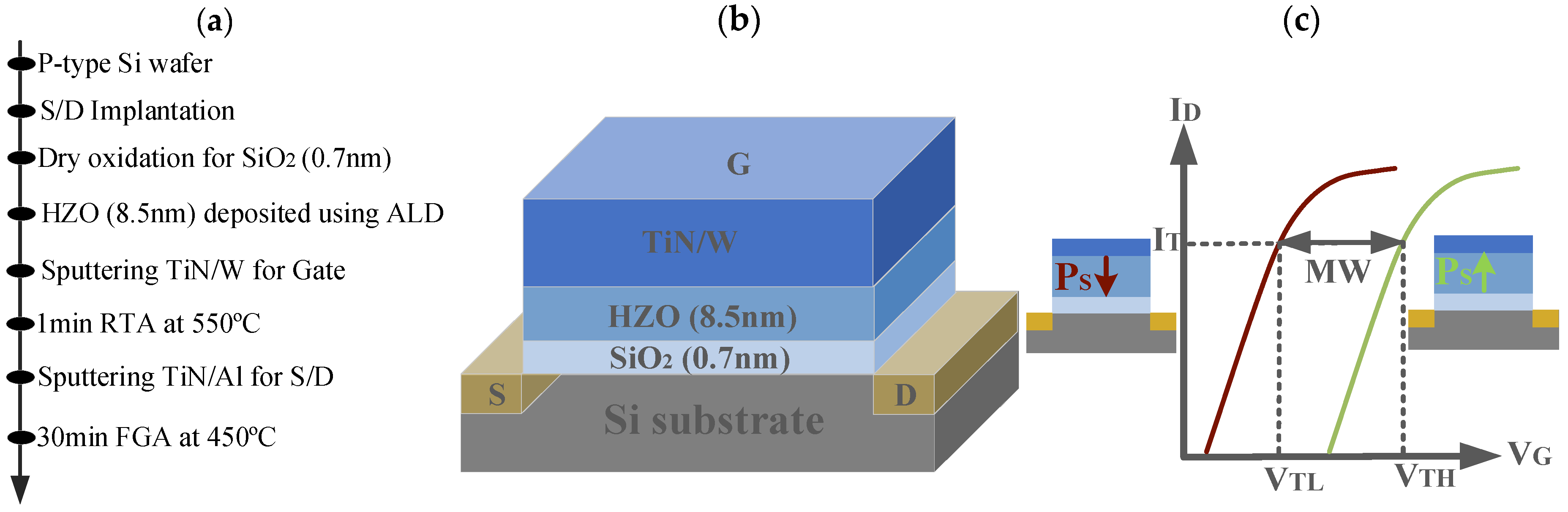
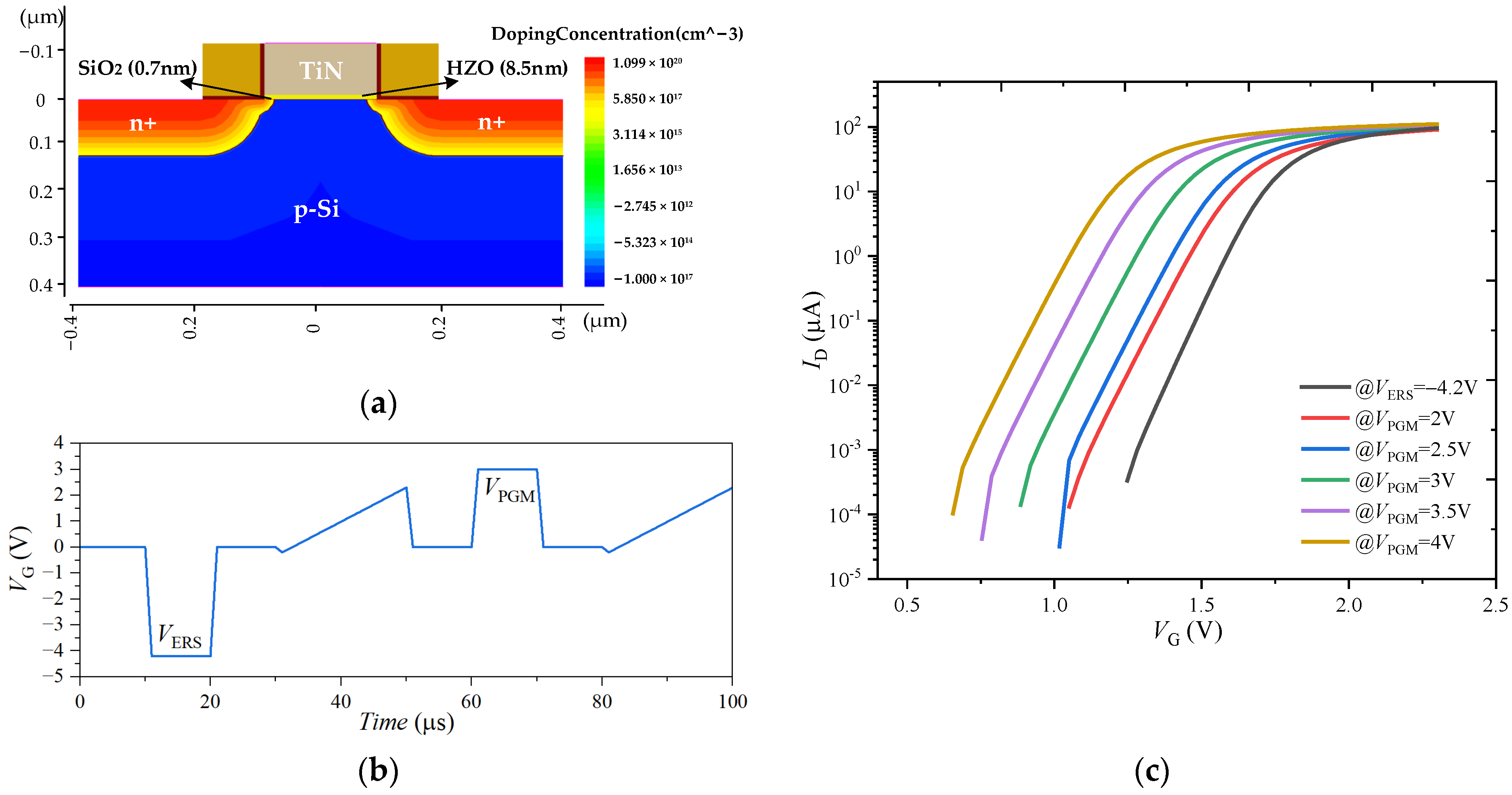
2. Devices and Methods

An n-channel FeFET with W/TiN/HZO/SiO2/Si gate stacks is fabricated on 8-inch p-Si (100) substrates using a gate-last process. Figure 1a,b show the key process steps and structure for the fabricated devices. The fabrication starts from the p-type Si substrate, and the Source (S) and Drain (D) are formed by implanting As ions. After that, an SiO2 insulator layer 0.7 nm thick is grown by oxidation in the O3 atmosphere. An HZO film 8.5 nm thick is formed by atomic layer deposition (ALD). The SiO2 layer and the HZO layer constitute the gate dielectric films. Then, TiN/W and TiN/Al are, respectively, deposited by sputtering as the gate metal and S and D metal. The HZO film is crystallized by rapid thermal annealing (RTA) in an N2 atmosphere at 550 °C for 60 s. Lastly, forming gas annealing (FGA) is performed.
The electrical characteristics of the FeFET device are measured using Agilent B1500A semiconductor device analyzer with SMUs and WGFMUs for DC and pulsed electrical measurements, respectively [24]. The gate width (W) and length (L) of the device used for MW tests are 150 μm and 10 μm, respectively. The memory effect in the FeFET depends on the polarization reversal in the gate stack. The polarization is downward or upward at a sufficiently large positive or negative gate voltage, respectively, corresponding to a low threshold voltage (VTL) state and a high threshold voltage (VTH) state [25]. The relationship between the transfer characteristic curves (ID-VG) and the polarization direction is shown in Figure 1c. The write operation is performed by applying PGM and ERS pulses, and the read operation is performed in a static scanning mode.
The gate stack consisting of a 10 nm thick TiN top gate electrode, an 8.5 nm thick HZO layer, and a 0.7 nm thick SiO2 layer on the substrate is confirmed by transmission electron microscopic (TEM), as shown in Figure 1c. It can be observed that the HZO layer is polycrystalline, indicating the multidomain structure in the HZO-based FeFETs. Moreover, the multilayer gate stack shows sharp interfaces, indicating that the high-quality film of FeFET device.
The crystal structures of the HZO films are also examined. Figure 2b presents X-ray diffraction (XRD) pictures of the FeFET. The measured peaks are well matched with the orthorhombic phase (PDF#83–0808) of the ferroelectric films. The XRD peaks are observed at the 2θ values of the superimposed orthogonal, indicating the ferroelectric properties of the prepared HfO2-based FeFET.
The X-ray photoelectron spectroscopy (XPS) of the HZO thin films is shown in Figure 3. The characteristic peaks of Hf 4f, Zr 3d, and O 1s are observed in the general survey spectra. Two components are identified at 16.9 and 18.6 eV corresponding to the hafnium oxide O–Hf–O bonds. Moreover, the Hf 4f doublet spin-orbit splitting and the peak intensity ratio are 1.7 eV and ∼0.73, respectively, in good agreement with the reported values [26]. Similarly, the Zr 3d spectrum consists of two spin-orbit splitting peaks at 182.5 and 184.9 eV. The energy splitting of 2.4 eV and the peak intensity ratio of ∼0.75 are consistent with Zr 3d found in the literature [27]. The ratio of the atomic percentage of Hf and Zr is about 1.05:1, indicating the Hf0.5Zr0.5O2 composition of the sample.

3. Experimental Results

3.1. Memory Window

Standard memory characteristics of the FeFET are measured using a pulse sequence as shown in Figure 4a: a pre-polarization pulse, a PGM pulse, an ID-VG read, an ERS pulse, and another ID-VG read [28]. In the figure, the amplitude of the PGM pulse is +4.5 V, and of the ERS pulse, −4.5 V; the pulse widths are 10 μs. The read ID-VG is measured from −1 V to 2.5 V taking 100 µs, and the drain voltage (VD) is set to VD = 100 mV. The ID-VG curves under the three conditions of no pulse (initial state), positive PGM pulse, and negative ERS pulse are tested and shown in Figure 4b. For the n-type FeFET, compared with the ID-VG curve in the initial state, the negative ERS pulse causes the ID-VG curve to shift to the right and the VT to increase, while the positive PGM pulse causes the ID-VG curve to shift to the left and the VT to decrease. This is because the polarization state of the ferroelectric film in the gate stack changes when the gate is applied with the PGM pulse and ERS pulse, resulting in a change in the threshold voltage of the FeFET. The MW value of the FeFET is obtained by extracting the threshold voltage difference (ΔVT) after the PGM and ERS pulses from the ID-VG curves. In this work, we define VT as the particular VG at which the ID = 10−7 × W/L A [29]. Figure 4b shows that the MW of the FeFET is 1.02 V (MW = VTHVTL). This shows that the fabricated FeFET device has good storage characteristics.
The IG-VG curves in Figure 4c show that, after applying the PGM and ERS pulse, the IG is larger than that in the initial state. The traps generated under the PGM and ERS pulses will trap electrons, and some electrons may enter the gate through the gate dielectric layer to form the gate leakage current, thus causing the IG increase after the PGM and ERS pulses, as compared with the initial state.

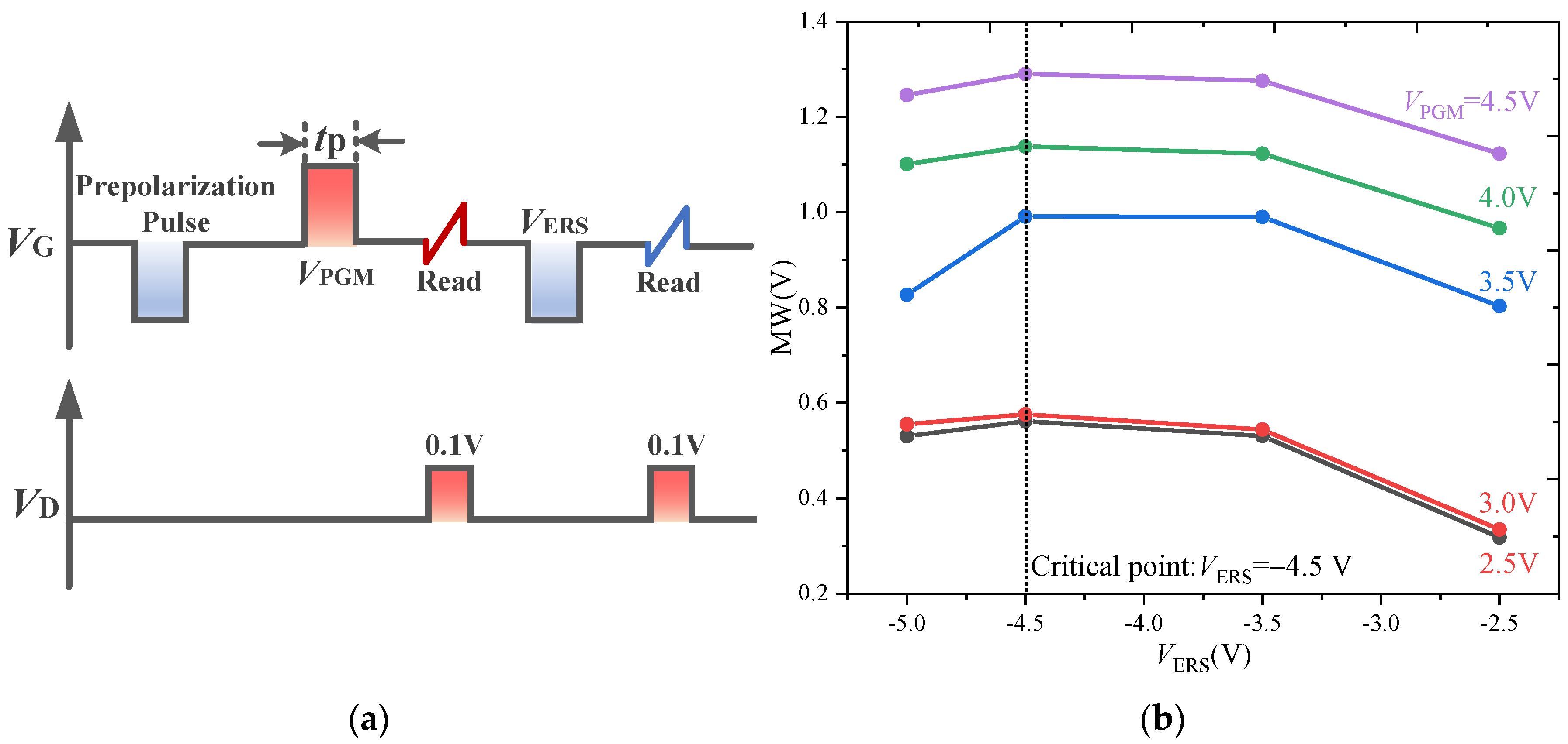
3.1.1. Memory Window under Various PGM and ERS Pulse Amplitudes

The influence of the CT on the MW is studied by changing the amplitudes of the PGM and ERS pulses (VPGM and VERS); the pulse sequence is shown in Figure 5a: the pulse width (tp) is 10 μs. The MW is plotted as functions of VERS for the various values of VPGM, as shown in Figure 5b.
Figure 5b shows that, under a given VPGM, the MW increases with the increase in |VERS|, but when |VERS| is greater than 4.5 V the MW decreases instead. For this result, the explanation is that the CT effect and FS effect act together on the FeFET, but their contributions to the MW are opposite. VERS = −4.5 V is the critical point. When |VERS| is less than 4.5 V, the polarization of the ferroelectric layer increases with the increase in |VERS| until it reaches the saturation state. In this process, the FS as the dominant effect causes the MW to gradually increase. Although |VERS| higher than 4.5 V will lead to further switching of the polarization, the increased CT effect in this voltage range overcompensates the influence of the ferroelectric polarization on the FeFET, resulting in a decrease in MW [28]. The relationship between CT and FS will be described in Section 3.2.

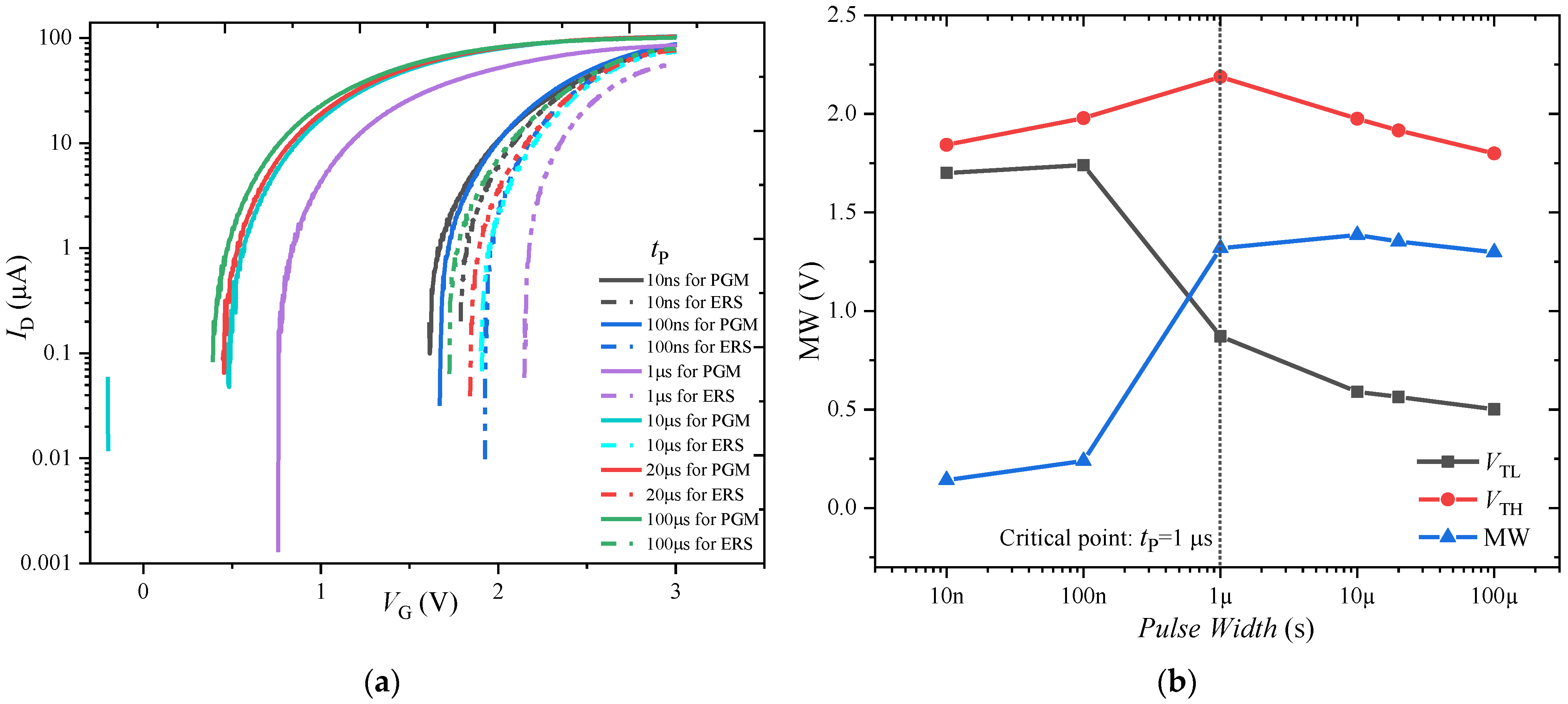
3.1.2. Memory Window under Various PGM and ERS Pulse Widths

The influence of the CT effect on the MW is studied by changing the width of the PGM and ERS pulses (tP). The pulse sequence is shown in Figure 5a. The pulse amplitude (VPGM/VERS) is ±4.5 V.
Figure 6a shows that the ID-VG curves under the various PGM pulse width values change greatly, and especially that tP = 1 μs is the critical point. When tP > 1 μs, the ID-VG curves under the PGM pulse shift significantly to the left. The variation of low threshold voltage (VTL), high threshold voltage (VTH) and MW value with respect to the pulse width are extracted according to the ID-VG curves, as shown in Figure 6b. When tP = 10 μs, the MW value reaches the maximum. The above phenomena can be explained by noting that in the PGM and ERS pulse sequence, the CT and FS act on the FeFET simultaneously, but compete. With the increase in the pulse width, the polarization will gradually completely reverse to increase the MW, and the probability of traps near the interface will also increase to weaken the MW. When tP < 1 μs, the short pulse duration limits the polarization switching process. With the increase in the pulse width, the polarization is gradually completely reversed, and the increase in the FS on the MW is stronger than the weakening of the CT on the MW, resulting in the increase in the MW with the increase in the pulse width. When tP > 10 μs, the polarization has reached the limit state of complete inversion, and the larger pulse width leads to more charge capture. The decrease in the MW due to the CT effect is stronger than the increase in the MW due to the FS effect, resulting in a slight reduction in the MW with the increase in the pulse width.

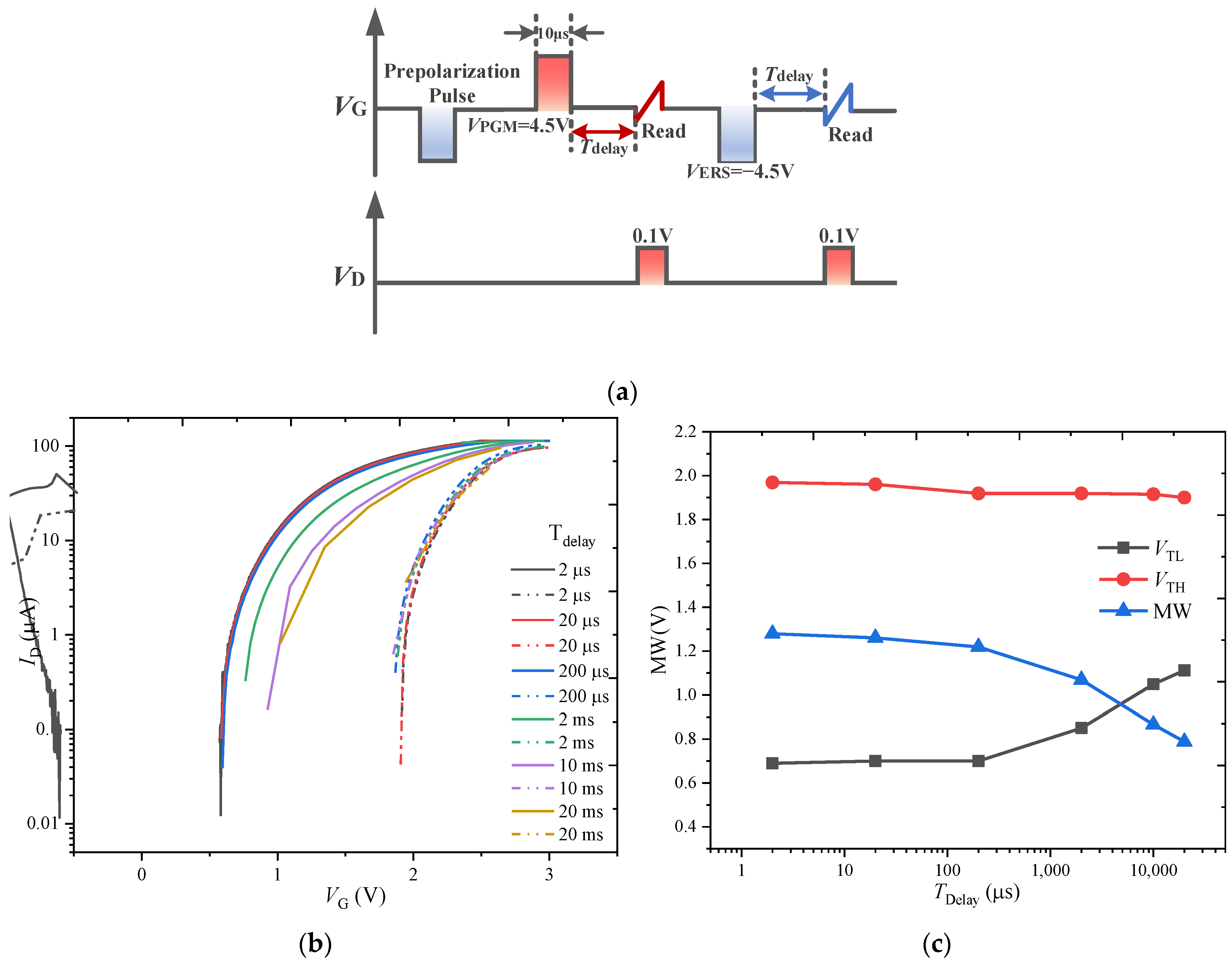
3.1.3. Memory Window under Various Read Delay Times

The time from the end of the write operation to the start of the read operation for the FeFET is defined as the read delay time (Tdelay). The effect of the read delay time on the MW is studied by applying the pulse sequence shown in Figure 7a. While the write pulses are fixed to ±4.5 V and 10 µs to ensure the complete switching of the polarization, the Tdelay is varied from 2 μs to 20 ms.
The ID-VG curves for various Tdelay are shown in Figure 7b. With the increase in Tdelay, the ID-VG curve after the PGM operation obviously shifts to the right, resulting in the reduction in the MW. Figure 7c shows the relationship between the VTL, VTH, and MW with Tdelay: VTH has no obvious change with the Tdelay, while VTL shows some retention degradation for Tdelay > 200 μs. The above phenomena can be explained by noting that there is reverse switching of ferroelectric domains under the depolarization field [20]; the number of reverse-switching domains increases with the increase in Tdelay, resulting in the reduction in the MW. However, the significant difference between the ID-VG curves under the PGM and ERS pulses with the increase in Tdelay indicates that the depolarization field is not the main reason for the decrease in MW. On the other hand, the traps generated under the programming and erasing pulses have more chances to capture the charge with the increase in Tdelay, resulting in the reduction in the MW. In addition, the difference in the change degree of VTH and VTL with Tdelay is caused by the differing abilities to generate traps under the PGM and ERS pulses.

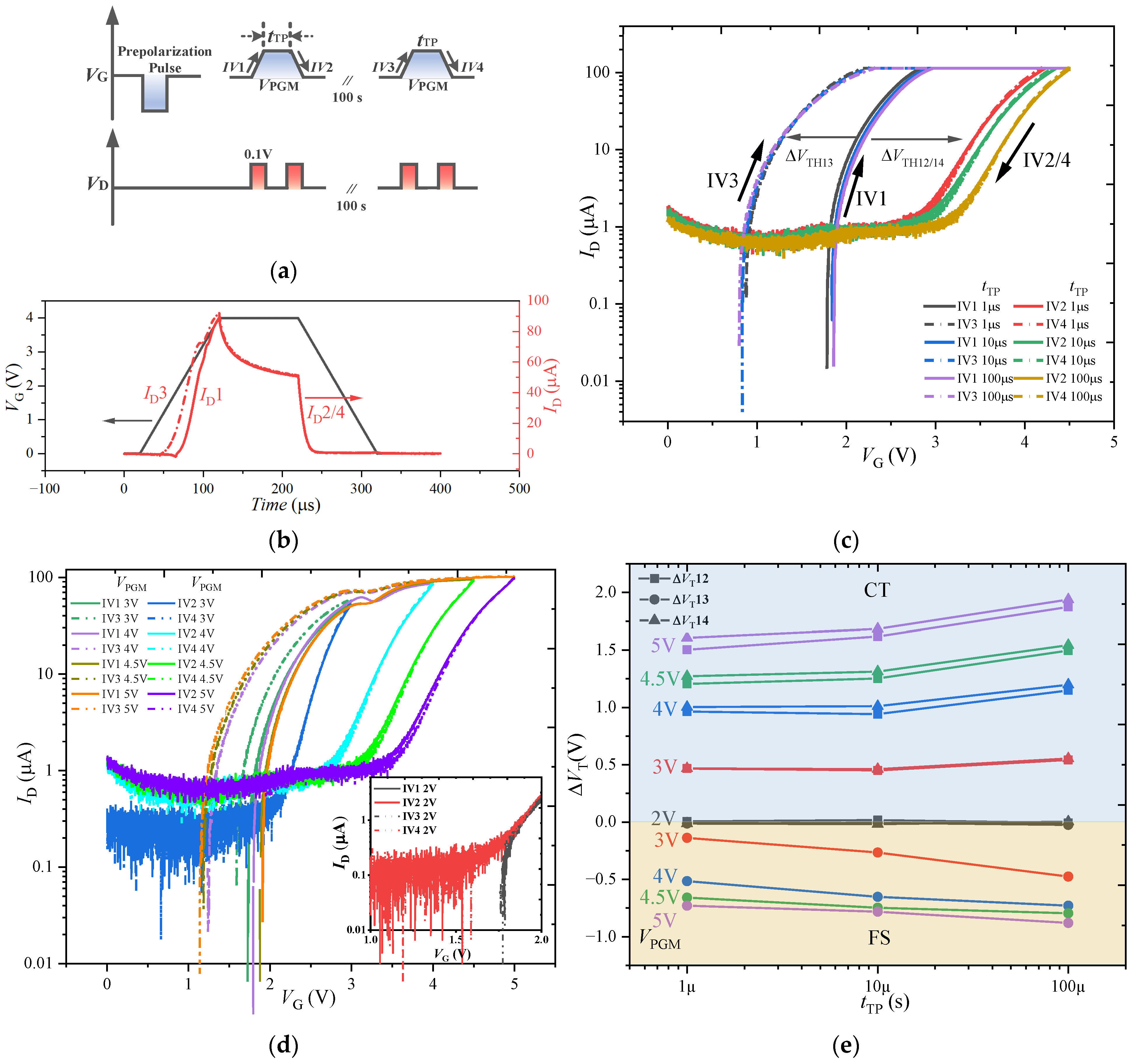
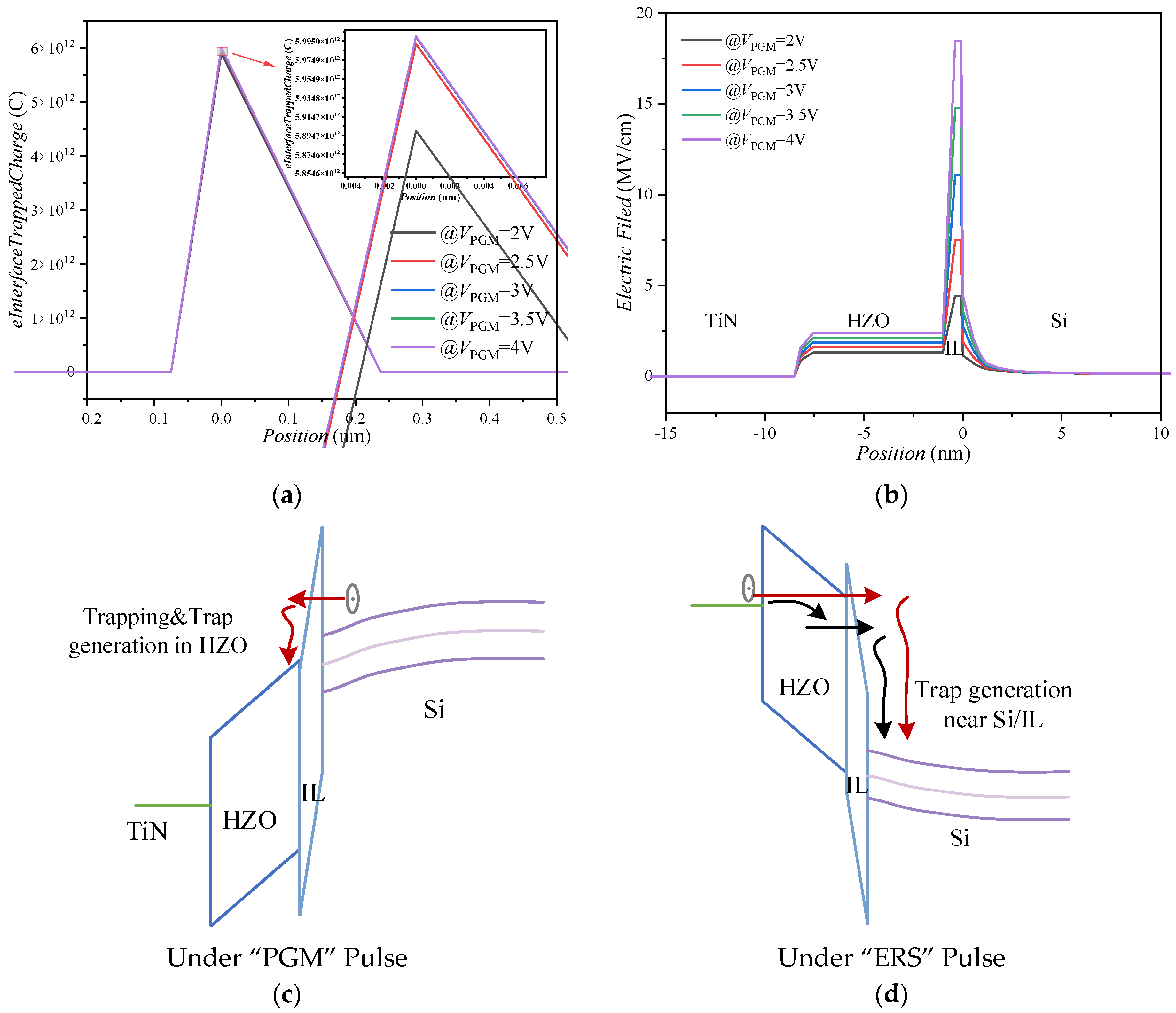
3.2. Charge Trapping and Ferroelectric Switching Effect

The FS and CT effects occur simultaneously in the FeFET. The contributions of these two effects to the MW are opposite: Under the positive PGM pulse, the CT leads the VT shift to the right, the FS leads the VT shift to the left; under the negative ERS pulse, the CT leads the VT shift to the left, the FS leads the VT shift to the right. Therefore, the superposition of the two effects will lead to the reduction in the MW of the FeFET. The competition between the FS and CT in the FeFET is studied by using the single-pulse ID-VG method [21]. The gate-pulse sequence shown in Figure 8a is used for this purpose. A first negative pulse (−4.5 V, 10 µs) is applied to establish a negative saturation polarization state, and two consecutive positive amplitude single pulses are applied to analyze the CT effect superimposed on the ferroelectric polarization switching. The specific test principle is as follows. During the first positive pulse, the dominant mechanism is determined by the VT offset between the ID-VG curves obtained on the rising edge (IV1) and the falling edge (IV2) of the pulse: if ΔVT < 0, the FS dominates; if ΔVT > 0, the CT dominates. After the first positive pulse, the FeFET is in a positive polarization state, and the dominant mechanism is determined according to the VT offset between the ID-VG curves obtained on the rising edge of the second pulse (IV3) and the rising edge of the first pulse (IV1). The purpose of 100 s interval between two single pulses is to recover the captured charge.
Figure 8b shows the corresponding current transient response when two single pulses (VPGM = 4.5 V, tTP = 10 µs) are applied to the gate, wherein the black solid line is the applied two single pulses (two pulses coincide), the red solid line ID1 corresponds to the rising edge IV1, and the red dotted line ID3 corresponds to the rising edge IV3. ID2 and ID4 correspond to falling edges IV2 and IV4. Figure 8b shows that ID3 is shifted to the left relative to ID1, and ID2 and ID4 are almost coincident.
The tTP and VPGM of the two single pulses in Figure 8a are changed to analyze the competitive relationship between the CT and FS, multiple groups of ID-VG curves varying with tTP and VPGM are obtained, as shown in Figure 8c,d, respectively. For Figure 8c, IV2 shifts to the right relative to IV1 during the first positive pulse, ΔVT12 = VT2 − VT1 > 0 (VT1 and VT2 represent the threshold voltages extracted from the IV1 curve and the IV2 curve, respectively), indicating that the CT dominates the threshold voltage shift. During the second positive pulse, IV3 shifts to the left relative to IV1, ΔVT13 = VT3 − VT1 < 0, indicating that the polarization switching dominates the threshold voltage shift. In addition, ΔVT12 increases with the increase in tTP, indicating that the trapped charge increases; ΔVT13 has almost no change with the increase in tTP, which further indicates that after the first pulse is applied, the FS dominates the change of threshold voltage rather than the charge detrapping.
For Figure 8d, the ID-VG curves have no obvious shift when the VPGM ≤ 2 V, as shown in the inset, indicating that the CT and FS effect of the FeFET are not significant under small VPGM. IV2/4 and IV3 are significantly shifted in opposite directions relative to IV1 with the increase in the VPGM. This shows that the CT and FS effect exist simultaneously. However, when the VPGM ≥ 4.5 V, the offset of IV3 relative to IV1 does not obviously increase with the increase in VPGM, while the offset of IV2/4 relative to IV1 still increases with the increase in VPGM. This indicates that the CT effect will be the dominant mechanism of the change of the MW for the FeFET when the pulse amplitude is greater than 4.5 V. The relationship between VPGM and ΔVT is summarized in Table 1, where the symbol “↑” in the table indicates ΔVT increase It can also explain that in Section 3.1.1, when |VERS| > 4.5 V, the MW value decreases instead with the increase in the pulse amplitude.
Figure 8e summarizes the variation of ΔVT with respect to tTP for various values of VPGM, where ΔVT12 and ΔVT14 increase with the increase in the pulse width under the various amplitudes, indicating that the amount of the trapped charge increases. In addition, |ΔVT13| increases significantly with the increase in the tTP when the VPGM = 3 V, indicating that the tTP also limits the inversion of the ferroelectric domain under the small VPGM. The most important thing is that |ΔVT13| does not increase significantly when the VPGM increases to 4.5 V, indicating that the CT effect plays a dominant role in the FeFET compared with the FS effect at large pulse amplitude.

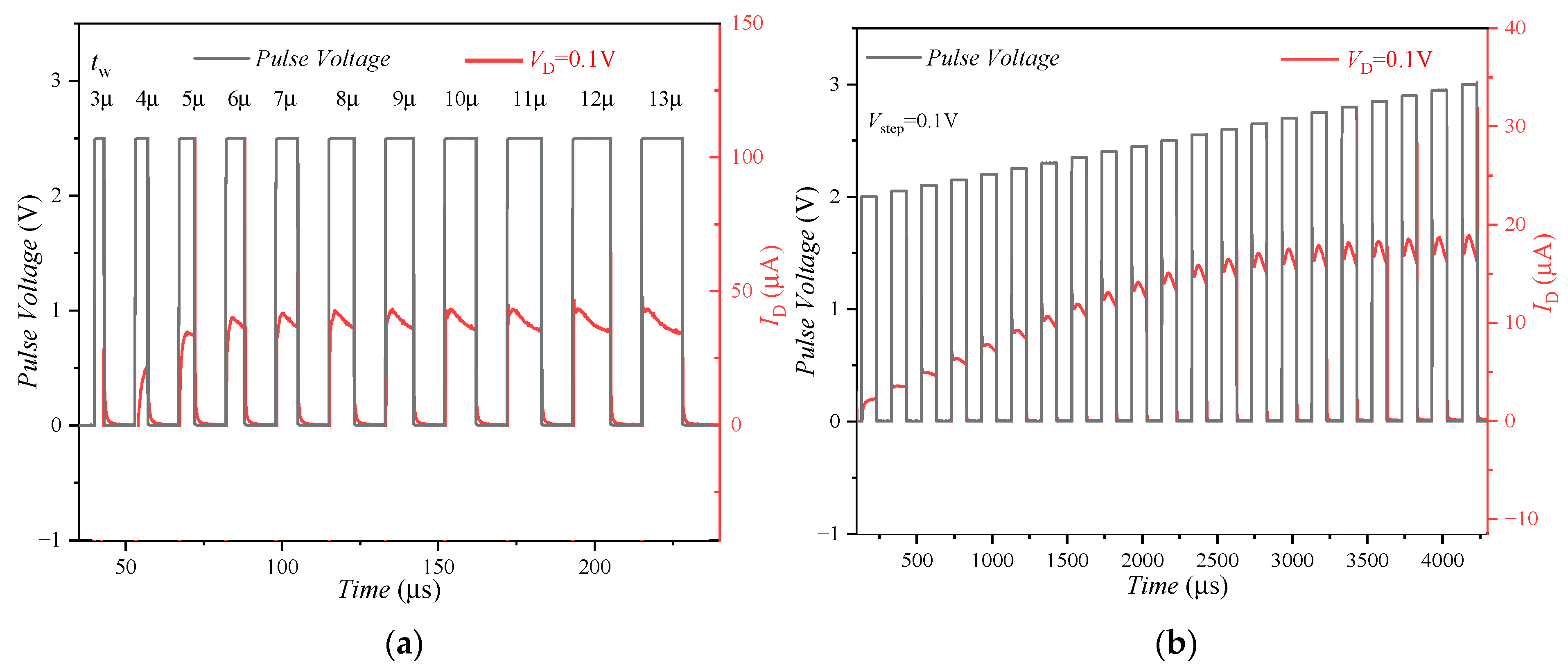
3.3. Conductance Modulation Characteristic Influenced by Charge Trapping Effect

The potential of the FeFET to exhibit analog synapses behavior has been investigated by the pulse width and amplitude modulation scheme in [30,31,32,33]. However, the experimental data in this work show that the channel conductance modulated by the pulse width and pulse amplitude will also be affected by the CT effect. The gate of the FeFET is applied with a pulse sequence that continuously increases the pulse width, and the drain of the FeFET is applied with a voltage of 0.1 V to read the drain current value, as shown in Figure 9a. When the pulse width is small, the FS effect dominates, and the drain current (ID) increases with the increase in the number of pulses, showing the potentiation characteristic; With the increase in the pulse width, the probability of the charge capture increases, and the CT effect increases gradually, which inhibits the increase in the ID, that is, the potentiation characteristics of the FeFET are suppressed.
Similarly, when a pulse sequence with a continuously increasing pulse amplitude is applied to the gate of the FeFET, as shown in Figure 9b, the ID increases with the number of pulses, FS is the dominant effect, showing the potentiation characteristic. When all domains in the ferroelectric layer are reversed, the polarization in the ferroelectric layer reaches the saturation state, and the current will not increase. However, during the process of the pulse application, the ID has a peak value, which can be explained as follows: with the increase in the pulse application time, the CT effect becomes the dominant mechanism, leading to the reduction in the ID.

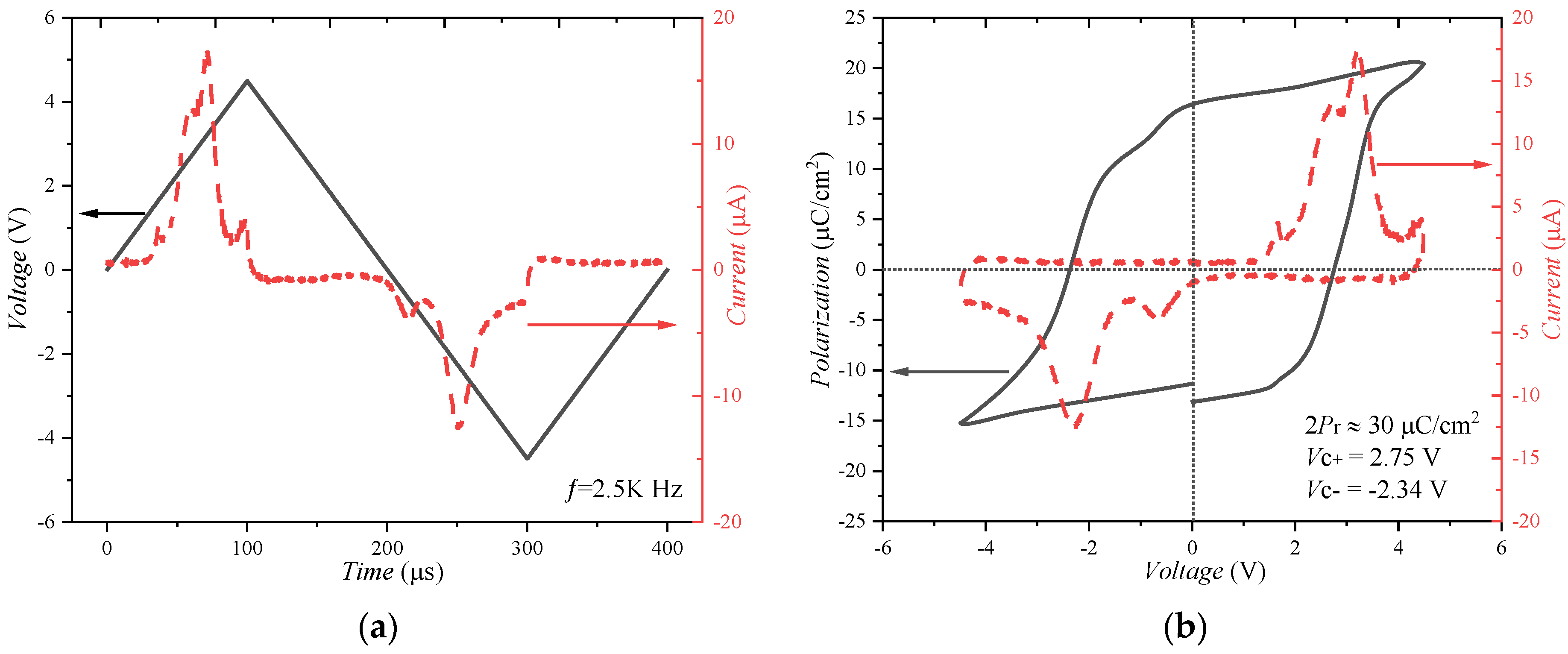
3.4. P-V Characteristics
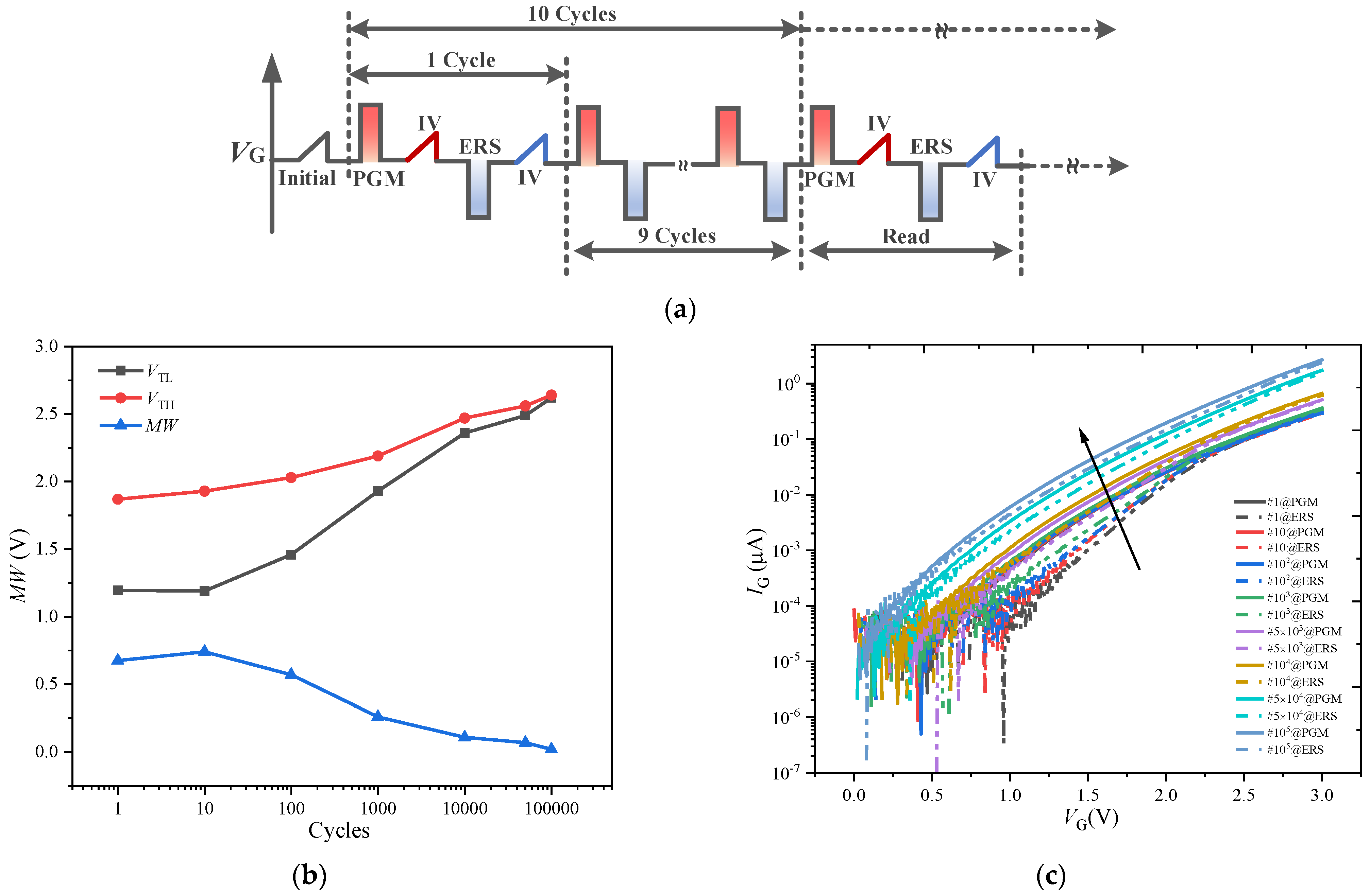
The P-V characteristics are measured by applying a triangular pulse sequence to the gate of the FeFET at 2.5 kHz as shown by the black solid line in Figure 10a, and short the Source, Drain, and substrate to the ground [28,34,35]. The maximum values of the triangular pulse sequence are VP = 4.5 V and VN = −4.5 V, respectively. The transient current response of a ferroelectric capacitor under triangular excitation gate voltage is shown by the red dotted line in Figure 10a. There are two characteristic current peaks in the current versus the time curve, corresponding to the domain switching under the coercive voltage (VC).
The polarization measurement is actually a measurement of charge in the capacitor given by Equation (1) [34,36].
Q = P A
where Q is the total charge in the ferroelectric, A is the capacitor area, and P is the polarization. Polarization can thus be obtained by the integration of the measured switching current (I) with respect to time, as shown in Equation (2) [34,36].
P = I d t A
The Polarization–Voltage (P-V) curve and Current–Voltage (I-V) are shown in Figure 10b. The P-V curve shows a typical polarization hysteresis loop with a dual remanent polarization (2Pr) value of 30 μC/cm2, and a positive and negative coercive voltage of 2.75 V and −2.34 V, respectively. The clear polarization switching behavior can be observed in the P-V curve. The Current–Voltage curve shows a single loop hysteresis with two consistent peaks, which is also a typical characteristic of ferroelectric materials [28].

3.5. Endurance

The endurance of the FeFET is tested by applying a pulse sequence with a VPGM = 4 V, VERS = −4 V and tp = 1 μs to the gate as shown in Figure 11a. The ID-VG curve is tested after applying the PGM and ERS pulses, and the threshold voltage is extracted from the ID-VG curve. Figure 11b shows the degradation relationship of the MW with the number of cycles. Both the VTH and VTL increase with the number of cycles, which is attributed to the CT effect [22]. When the number of cycles reaches 105, the MW almost disappears.
Figure 11c shows the relationship between the gate current and the gate voltage (IG-VG) under various cycles. When the number of cycles reaches 104, the gate current increases significantly. When the number of cycles reaches 105, the IG increases by an order of magnitude compared with the initial state.

4. Discussion

To provide a plausible explanation of the CT behavior in the FeFET, a theoretical investigation is performed in Sentaurus TCAD. The FeFET structure, as shown in Figure 12a, is built with the p-type Si substrate, a 0.7 nm SiO2 interlayer, an HZO ferroelectric 8.5 nm thick, and TiN metal. The ferroelectric is described with the dynamic Preisach model [37], and the model parameters are consistent with the measured experimental data of the FeFET, Pr is 15 μC/cm2, Ps is 20 μC/cm2, and Ec is 2.5 MV/cm. Acceptor-type traps (Trap density = 1 × 1013 cm−3) are injected at the channel/interface layer of the FeFET for the TCAD simulation [38]. The pulse scheme shown in Figure 12b is used for the simulation of the FeFET MW, and the amplitude of the programming pulse is changed to evaluate the impact of the CT on the MW.
Under a fixed erasing pulse amplitude (VERS = 4.2 V), the MW increases with the increase in the amplitude of the VPGM pulse, as shown in Figure 12c. This is because with the increase in the PGM amplitude, the polarization intensity in the ferroelectric layer gradually increases, resulting in the shift of the ID-VG curves’ decrease in the threshold voltage. In this process, the FS effect is the dominant mechanism, which is consistent with the test results of the FeFET.
The CT effect in the process of increasing the amplitude for the PGM pulse is further analyzed. When the amplitude of the VPGM increases from 2 V to 2.5 V, the number of charges trapped by the interface traps increases significantly, as shown in the inserted figure in Figure 13a, which counteracts the ability of the FS effect to increase the MW, resulting in a slightly smaller increase in the MW. When the VPGM is greater than 2.5 V, the number of trapped charges in the interface still increases, but the FS effect, as the dominant mechanism, makes the MW significantly increased. From the simulation results and experimental data, it can be seen that the CT effect strongly depends on the pulse conditions applied by the gate. In order to reduce the impact of the CT effect on the FeFET MW and increase the endurance of the device, appropriate programming and erasing conditions can be designed.
The variations of electric field strength in the ferroelectric layer and interface layer with the amplitude of VPGM are shown in Figure 13b. The interlayer electric field is strengthened by the polarization pointing at the channel under the PGM pulse. It will facilitate the electron injection into the gate stack.
Figure 13c,d show the energy band diagram under the PGM and ERS pulse train, respectively. During the PGM pulse, electrons tunnel through the interface layer (IL) and enter the HZO region. Energy will be lost in this process, which will generate border traps near the HZO/IL interface [22]. However, some electrons may be trapped; during the ERS pulse, electrons flow through HZO by Fowler–Nordheim (FN) or by trap-assisted conduction and remain “hot” when entering the Si interface. Some of them may generate interface traps while losing energy. Traps generated under the PGM and ERS pulse will capture charges. The number of traps generated and charges captured is related to the amplitude and width of the PGM and ERS pulse, which compete with the FS effect and affect the memory window of the FeFET.

5. Conclusions

The effect of CT on the performance of W/TiN/HZO/SiO2/Si gate stacked FeFET devices is studied. The competition between CT and FS is analyzed by a single-pulse technique. When the amplitude of the single-pulse is increased to 4.5 V, the contribution of CT is stronger than that of FS for the FeFET, and the MW is reduced. Due to the CT effect, the endurance cycle of the FeFET is only 105. In addition, in the analog synaptic behavior of the FeFET, the conductance modulation characteristics are also affected by the CT effect, and the continuous increase in conductance is inhibited. The simulation results of Sentaurus TCAD explain the mechanism of the CT effect on the MW of the FeFET. This work lays a foundation for the study of alleviating the endurance fatigue process caused by the CT effect and enhancing the analog synaptic behavior of the FeFET.

Author Contributions

Conceptualization, J.W. and J.B.; methodology, J.W.; software, J.W. and Y.X.; formal analysis, J.W.; investigation, J.W.; resources, J.B. and G.N.; data curation, J.B.; writing—original draft preparation, J.W.; writing—review and editing, J.W.; supervision, J.B., M.L. and V.S.; project administration, J.B.; funding acquisition, J.B. All authors have read and agreed to the published version of the manuscript.

Funding

This research was funded by National Key Research and Development Program of China (No. 2022YFE0124200) and National Natural Science Foundation of China (No. U2241221).

Data Availability Statement

Not applicable.

Conflicts of Interest

The authors declare no conflict of interest.

References

  1. Boscke, T.; Muller, J.; Brauhaus, D.; Schroder, U.; Bottger, U. Ferroelectricity in Hafnium Oxide Thin Films. Appl. Phys. Lett. 2011, 99, 102903. [Google Scholar] [CrossRef]
  2. Wang, J.; Bi, J.; Liu, G.; Bai, H.; Xi, K.; Ji, L.; Li, B.; Majumdar, S. Simulations of Single Event Effects in 6T2C-based Ferroelectric Non-volatile SRAM. Semicond. Sci. Technol. 2020, 36, 015015. [Google Scholar] [CrossRef]
  3. Zhao, B.; Yan, Y.; Bi, J.; Xu, G.; Xu, Y.; Yang, X.; Fan, L.; Liu, M. Improved Ferroelectric Properties in Hf0.5Zr0.5O2 Thin Films by Microwave Annealing. Nanomaterials 2022, 12, 3001. [Google Scholar] [CrossRef]
  4. Van, J. 3D Memories and Ferroelectrics. In Proceedings of the 2017 IEEE International Memory Workshop (IMW), Monterey, CA, USA, 14–17 May 2017; pp. 1–3. [Google Scholar]
  5. Dunkel, S.; Trentzsch, M.; Richter, R.; Moll, P.; Fuchs, C.; Gehring, O.; Majer, M.; Wittek, S.; Müller, B.; Melde, T.; et al. A FeFET based Super-Low-Power Ultra-Fast Embedded NVM Technology for 22 nm FDSOI and Beyond. In Proceedings of the 2017 IEEE International Electron Devices Meeting (IEDM), San Francisco, CA, USA, 2–6 December 2017; pp. 19.7.1–19.7.4. [Google Scholar]
  6. Florent, K.; Lavizzari, S.; Di Piazza, L.; Popovici, M.; Vecchio, E.; Potoms, G.; Groeseneken, G.; Van Houdt, J. First Demonstration of Vertically Stacked Ferroelectric Al Doped HfO2 Devices for NAND Applications. In Proceedings of the 2017 Symposium on VLSI Technology, Kyoto, Japan, 5–8 June 2017. [Google Scholar]
  7. Yang, X.; Xu, Y.; Bi, J.; Fan, L.; Ji, L.; Xu, G. Total Ionizing Dose Effects on Aluminum Oxide/Zirconium-Doped Hafnium Oxide Stack Ferroelectric Tunneling Junctions. Sci. China Inf. Sci. 2021, 64, 279–280. [Google Scholar] [CrossRef]
  8. Yang, X.; Bi, J.; Xu, Y.; Xi, K.; Ji, L. The Effects of Proton Radiation on Aluminum Oxide/Zirconium-Doped Hafnium Oxide Stacked Ferroelectric Tunneling Junctions. Appl. Phys. Express 2021, 14, 061001. [Google Scholar] [CrossRef]
  9. Yan, G.; Xu, G.; Bi, J.; Tian, G.; Xu, Q.; Yin, H.; Li, Y. Accumulative Total Ionizing Dose (TID) and Transient Dose Rate (TDR) Effects on Planar and Vertical Ferroelectric Tunneling-Field-Effect-Transistors (TFET). Microelectron. Reliab. 2020, 114, 113855. [Google Scholar] [CrossRef]
  10. Tian, G.; Bi, J.; Xu, G.; Xi, K.; Yang, X.; Yin, H.; Wang, W. Heavy Ion Induced Single-Event-Transient Effects in Nano-Scale Ferroelectricity Vertical Tunneling Transistors by TCAD Simulation. Semicond. Sci. Technol. 2020, 35, 105010. [Google Scholar] [CrossRef]
  11. Choe, G.; Yu, S. Variability Study of Ferroelectric Field-Effect Transistors Towards 7nm Technology Node. IEEE J. Electron. Dev. 2021, 9, 1131–1136. [Google Scholar] [CrossRef]
  12. Xiao, W.; Liu, C.; Peng, Y.; Zheng, S.; Feng, Q.; Zhang, C.; Zhang, J.; Hao, Y.; Liao, M.; Zhou, Y. Performance Improvement of Hf0.5Zr0.5O2 based Ferroelectric-Field-Effect Transistors with ZrO2 Seed Layers. IEEE Electron Device Lett. 2019, 40, 714–717. [Google Scholar] [CrossRef]
  13. Tian, G.; Bi, J.; Xu, G.; Xi, K.; Yang, X.; Majumdar, S.; Yin, H.; Xu, Q.; Wang, W. Single-Event-Transient Effects in Silicon-on-Insulator Ferroelectric Double-Gate Vertical Tunneling field Effect Transistors. Sci. China Inf. Sci. 2020, 63, 229403. [Google Scholar] [CrossRef]
  14. Breyer, E.; Mulaosmanovic, H.; Mikolajick, T.; Slesazeck, S. Reconfigurable NAND/NOR Logic Gates in 28 nm HKMG and 22 nm FD-SOI FeFET Technology. In Proceedings of the 2017 IEEE International Electron Devices Meeting (IEDM), San Francisco, CA, USA, 2–6 December 2017; pp. 28.5.1–28.5.4. [Google Scholar]
  15. Deng, S.; Jiang, Z.; Dutta, S.; Ye, H.; Chakraborty, W.; Santosh, K.; Datta, S.; Ni, K. Examination of the Interplay between Polarization Switching and Charge Trapping in Ferroelectric FET. In Proceedings of the 2020 IEEE International Electron Devices Meeting (IEDM), San Francisco, CA, USA, 12–18 December 2020; pp. 4.4.1–4.4.4. [Google Scholar]
  16. Deng, S.; Zhao, Z.; Sung, Y.; Duenkel, S.; MacMahon, D.; Tiwari, R.; Choudhury, N.; Beyer, S.; Gong, X.; Kurinec, S.; et al. Unraveling the Dynamics of Charge Trapping and De-Trapping in Ferroelectric FETs. IEEE Trans. Electron Devices 2022, 69, 1503–1511. [Google Scholar] [CrossRef]
  17. Toprasertpong, K.; Lin, Z.; Lee, T.; Takenaka, M.; Takagi, S. Asymmetric Polarization Response of Electrons and Holes in Si FeFETs Demonstration of Absolute Polarization Hysteresis Loop and Inversion Hole Density over 2 × 1013 cm2. In Proceedings of the 2020 IEEE Symposium on VLSI Technology, Honolulu, HI, USA, 16–19 June 2020; pp. 1–2. [Google Scholar]
  18. Izmailov, R.; Strand, J.; Larcher, L.; O’Sullivan, B.; Shluger, A.; Afanas’ev, V. Electron Trapping in Ferroelectric HfO2. Phys. Rev. Mater. 2021, 5, 034415. [Google Scholar] [CrossRef]
  19. Ali, T.; Polakowski, P.; Riedel, S.; Büttner, T.; Kämpfe, T.; Rudolph, M.; Pätzold, B.; Seidel, K.; Löhr, D.; Hoffmann, R.; et al. High Endurance Ferroelectric Hafnium Oxide-based FeFET Memory without Retention Penalty. IEEE Trans. Electron Devices 2018, 65, 3769–3774. [Google Scholar] [CrossRef]
  20. Hoffmann, M.; Tan, A.; Shanker, N.; Liao, Y.; Wang, L.; Bae, J.; Hu, C.; Salahuddin, S. Fast Read-After-Write and Depolarization Fields in High Endurance n-Type Ferroelectric FETs. IEEE Electron Device Lett. 2022, 43, 1–4. [Google Scholar] [CrossRef]
  21. Yurchuk, E.; Müller, J.; Müller, S.; Paul, J.; Peši’c, M.; Bentum, R.; Schroeder, U.; Mikolajick, T. Charge-Trapping Phenomena in HfO2-Based FeFET-Type Nonvolatile Memories. IEEE Trans. Electron Device 2016, 63, 3501–3507. [Google Scholar] [CrossRef]
  22. Gong, N.; Ma, T. A Study of Endurance Issues in HfO2-Based Ferroelectric Field Effect Transistors: Charge Trapping and Trap Generation. IEEE Electron Device Lett. 2018, 39, 15–18. [Google Scholar] [CrossRef]
  23. Higashi, Y.; Ronchi, N.; Kaczer, B.; Banerjee, K.; McMitchell, S.; O’Sullivan, B.; Clima, S.; Minj, A.; Celano, U.; Piazza, L.; et al. Impact of Charge Trapping on Imprint and its Recovery in HfO2 based FeFET. In Proceedings of the 2019 IEEE International Electron Devices Meeting (IEDM), San Francisco, CA, USA, 7–11 December 2019; pp. 15.6.1–15.6.4. [Google Scholar]
  24. Zeng, B.; Xiao, W.; Liao, J.; Liu, H.; Liao, M.; Peng, Q.; Zheng, S.; Zhou, Y. Compatibility of HfN Metal Gate Electrodes with Hf0.5Zr0.5O2 Ferroelectric Thin Films for Ferroelectric Field-Effect Transistors. IEEE Electron Device Lett. 2018, 39, 1508–1511. [Google Scholar] [CrossRef]
  25. Mulaosmanovic, H.; Dunkel, S.; Muller, J.; Trentzsch, m.; Beyer, S.; Breyer, E.; Mikolajick, T.; Slesazeck, S. Impact of Read Operation on the Performance of HfO2-based Ferroelectric FETs. IEEE Electron Device Lett. 2020, 41, 1420–1423. [Google Scholar] [CrossRef]
  26. Sharath, S.; Bertaud, T.; Kurian, J.; Hildebrandt, E.; Walczyk, C.; Calka, P.; Zaumseil, P.; Sowinska, M.; Walczyk, D.; Gloskovskii, A.; et al. Towards Forming-free Resistive Switching in Oxygen Engineered HfO2−x. Appl. Phys. Lett. 2014, 104, 063502. [Google Scholar] [CrossRef]
  27. Hachemi, M.; Salem, B.; Consonni, V.; Roussel, H.; Garraud, A.; Lefevre1, G.; Labau, S.; Basrour, S.; Bsiesy, A. Study of Structural and Electrical Properties of Ferroelectric HZO Films Obtained by Single-Target Sputtering. AIP Adv. 2021, 11, 085004. [Google Scholar] [CrossRef]
  28. Tasneem, N.; Islam, M.; Wang, Z.; Zhao, Z.; Upadhyay, N.; Lombardo, S.; Chen, H.; Hur, J.; Triyoso, D.; Consiglio, S.; et al. Efficiency of Ferroelectric Field-Effect Transistors: An Experimental Study. IEEE Trans. Electron Device 2022, 69, 1568–1574. [Google Scholar] [CrossRef]
  29. Toprasertpong, K.; Tahara, K.; Fukui, T.; Lin, Z.; Watanabe, K.; Takenaka, M.; Takagi, S. Improved Ferroelectric/Semiconductor Interface Properties in Hf0.5Zr0.5O2 Ferroelectric FETs by Low-Temperature Annealing. IEEE Electron Device Lett. 2020, 41, 1588–1591. [Google Scholar] [CrossRef]
  30. Jerry, M.; Chen, P.; Zhang, J.; Sharma, P.; Ni, K.; Yu, S.; Datta, S. Ferroelectric FET Analog Synapse for Acceleration of Deep Neural Network Training. In Proceedings of the 2017 IEEE International Electron Devices Meeting (IEDM), San Francisco, CA, USA, 2–6 December 2017; pp. 6.2.1–6.2.4. [Google Scholar]
  31. Liu, H.; Li, J.; Wang, G.; Chen, J.; Yu, X.; Liu, Y.; Jin, C.; Wang, S.; Hao, Y.; Han, G. Analog Synapses based on Nonvolatile FETs with Amorphous ZrO2 Dielectric for Spiking Neural Network Applications. IEEE Trans. Electron Device. 2022, 69, 1028–1033. [Google Scholar] [CrossRef]
  32. Jerry, M.; Dutta, S.; Kazemi, A.; Ni, K.; Zhang, J.; Chen, P.; Sharma, P.; Yu, S.; Hu, X.; Niemier, M.; et al. A Ferroelectric Field Effect Transistor based Synaptic Weight Cell. J. Phys. D Appl. Phys. 2018, 51, 434001. [Google Scholar] [CrossRef]
  33. Kim, M.; Lee, J. Ferroelectric Analog Synaptic Transistors. Nano Lett. 2019, 19, 2044–2050. [Google Scholar] [CrossRef] [PubMed]
  34. Nam, K.; Park, J.; Kwon, K.; Choi, B. Charge Pumping Technique to Measure Polarization Switching Charges of FeFETs. IEEE Electron Device Lett. 2022, 69, 5289–5296. [Google Scholar] [CrossRef]
  35. Toprasertpong, K.; Tahara, K.; Takenaka, M.; Takagi, S. Evaluation of Polarization Characteristics in Metal/Ferroelectric/Semiconductor Capacitors and Ferroelectric Field-Effect Transistors. Appl. Phys. Lett. 2020, 116, 242903. [Google Scholar] [CrossRef]
  36. Rani, K. Switchable Photovoltaic Properties in Ferroelectric PZT Thin Films. Ph.D. Thesis, University of Saclay, Paris, France, 21 March 2022. [Google Scholar]
  37. Ni, K.; Jerry, M.; Smith, J.; Datta, S. A Circuit Compatible Accurate Compact Model for Ferroelectric-Fets. In Proceedings of the 2018 IEEE Symposium on VLSI Technology, Honolulu, HI, USA, 18–22 June 2018; pp. 131–132. [Google Scholar]
  38. Liu, Y.; Su, P. Comparison of 2-D MoS2 and Si Ferroelectric FET Nonvolatile Memories Considering the Trapped-Charge-Induced Variability. IEEE Trans. Electron Device 2022, 69, 2738–2740. [Google Scholar] [CrossRef]
Figure 1. (a) Key fabrication process steps and (b) schematic structure for the fabricated Hf0.5Zr0.5O2 (HZO) ferroelectric field effect transistor (FeFET) devices. (c) The transfer characteristic curves (ID-VG) under the opposite spontaneous polarization (PS) directions for the FeFET.
Nanomaterials 13 00638 g001
Figure 2. (a) Cross-sectional transmission electron microscope (TEM) image of the FeFET with gate stack of TiN/HZO/SiO2 on Si substrate. (b) The X-ray diffraction (XRD) pattern of the HZO thin films.
Nanomaterials 13 00638 g002
Figure 3. The XPS survey scan of the deposited 8.5 nm HZO layer.
Nanomaterials 13 00638 g003
Figure 4. (a) Pulse sequence used for finding the MW of the FeFET. (b) ID-VG and (c) IG-VG curves of FeFET after PGM pulse and ERS pulse compared with the initial state.
Nanomaterials 13 00638 g004
Figure 5. (a) Pulse sequence used for MW test at various VPGM of the FeFET. (b) Variation of MW with respect to VERS for various values of VPGM in FeFET.
Nanomaterials 13 00638 g005
Figure 6. (a) ID-VG characteristics of FeFET for varying PGM and ERS pulse widths. (b) Variation of VTL, VTH, and MW with respect to various values of pulse width in FeFET.
Nanomaterials 13 00638 g006
Figure 7. (a) Pulse sequence used for MW test at various Tdelay of the FeFET. (b) ID-VG characteristics of FeFET for varying Tdelay. (c) Variation of VTL, VTH, and MW at various values of Tdelay in FeFET.
Nanomaterials 13 00638 g007
Figure 8. (a) Pulse sequence with two single pulses used for CT and FS competition test of the FeFET. (b) Transient current response of FeFET under two single pulses: ID1 and ID3 correspond to the rising edges IV1 and IV3, ID2 and ID4 correspond to the falling edges IV2 and IV4. ID-VG characteristics measured on the rising (IV1) and falling (IV2) edges of the first single-pulse and the rising (IV3) and falling (IV4) edges of the second single-pulse (c) with various pulse widths, and (d) with various pulse amplitudes. (e) Variation of ΔVT with respect to tTP for various values of VPGM under two single pulses.
Nanomaterials 13 00638 g008
Figure 9. Effect of CT on (a) pulse width and (b) pulse amplitude modulation channel conductivity for FeFET. The gate of FeFET is applied with a pulse sequence with gradually increasing pulse width and pulse amplitude, and the drain current value is read out under a fixed drain voltage (VD = 0.1 V).
Nanomaterials 13 00638 g009
Figure 10. (a) Transient current response (red dotted line) of the FeFET under triangular excitation gate voltage (black solid line) during polarization measurements at a frequency of 2.5 kHz, and (b) resulting Current–Voltage (red dotted line) and Polarization–Voltage (black solid line) curve.
Nanomaterials 13 00638 g010
Figure 11. (a) Pulse sequence used for endurance measurements of the FeFET. (b) Variation of MW, VTH, and VTL with respect to cycles number. VTH and VTL increase with the increase in endurance cycles, the MW disappears at 105 cycles. (c) IG-VG curves under various endurance cycles, where the black arrow indicates that the gate current increases with the number of endurance cycles.
Nanomaterials 13 00638 g011
Figure 12. (a) Simulated structure of FeFET in Sentaurus TCAD. (b) Program/Erase pulse scheme along with the read cycle (sweep from −0.2 V to 2.5 V) for FeFET simulation. (c) Simulated ID-VG characteristics of FeFET for varying VPGM.
Nanomaterials 13 00638 g012
Figure 13. (a) Interface trapped charge varies with the voltage of program pulse. (b) Electrical field and conduction band diagram in FeFET using TCAD tools at the various voltages of the program pulse. Schematic diagram of energy band under (c) PGM and (d) ERS pulses, where the red and black arrows indicate that electrons flow through HZO through FN tunneling and trap-assisted conduction, respectively.
Nanomaterials 13 00638 g013
Table 1. Variation of ΔVT at various VPGM by the single-pulse ID-VG method.
VPGMΔVT12ΔVT13Dominant Role
≤2 V---
>2 V and ≤4.5 VCT and FS
>4.5 V-CT
Disclaimer/Publisher’s Note: The statements, opinions and data contained in all publications are solely those of the individual author(s) and contributor(s) and not of MDPI and/or the editor(s). MDPI and/or the editor(s) disclaim responsibility for any injury to people or property resulting from any ideas, methods, instructions or products referred to in the content.

