Abstract
Among photodetectors, avalanche photodiodes (APDs) have an important place due to their excellent sensitivity to light. APDs transform photons into electrons and then multiply the electrons, leading to an amplified photocurrent. APDs are promising for faint light detection owing to this outstanding advantage, which will boost LiDAR applications. Although Si APDs have already been commercialized, their spectral region is very limited in many applications. Therefore, it is urgently demanded that the spectral region APDs be extended to the short-wavelength infrared (SWIR) region, which means better atmospheric transmission, a lower solar radiation background, a higher laser eye safety threshold, etc. Up until now, both Ge (GeSn) and InGaAs were employed as the SWIR absorbers. The aim of this review article is to provide a full understanding of Ge(GeSn) and InGaAs for PDs, with a focus on APD operation in the SWIR spectral region, which can be integrated onto the Si platform and is potentially compatible with CMOS technology.
1. Introduction
Photodetectors convert the optical signal into an electrical signal, thereby amplifying the photocurrent through external or built-in gain processes. Generally, photodetector structures are classified as: photoconductors, PN photodiodes, PIN photodiodes, avalanche photodiodes (APDs), phototransistors, Schottky barrier photodiodes, metal-semiconductor-metal (MSM) photodiodes, etc. [1,2,3,4,5,6]. As a class of extremely sensitive semiconductor detectors, APDs are capable of multiplying the charge carriers via impact ionization, increasing the photocurrent that flows in response to a certain light power. The photocarriers generated by impact ionization can themselves initiate further impact ionization, resulting in the avalanche. When the reverse biased voltage is relatively small, APDs work in linear mode, and the electrical response is directly proportional to the incident light power, which makes linear mode APD is widely used in optical communication systems. However, increasing the reverse-biased voltage will push the APD into Geiger mode, for which the electrical response is non-linear. Thus, incident photons result in a large sudden voltage spike, indicating Geiger mode APDs as the most suitable for the photon counting system, and cryogenic cooling is unnecessary. Generally, APDs can be classified in terms of their operation wavelength range, compromising near-infrared (NIR, 0.78~1.1 μm), short-wavelength infrared (SWIR, 1.1–3 μm), mid-wavelength infrared (MWIR, 3–5 μm), and long-wavelength infrared (LWIR, 8–14 μm). Especially for the SWIR band, APDs have several potential applications, including optical communication, quantum information, range-finding, coherent sensing, medical diagnostics, analytical apparatus, vehicle light detection and ranging (LIDAR), life science, etc. (Figure 1) [7,8,9,10,11,12].
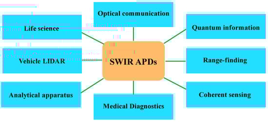
Figure 1.
Potential applications of SWIR APDs in various fields.
Among all the above-mentioned applications, vehicle LIDAR has the largest market share. With the rapid development of science and technology, vehicles have become an important part of daily life. In recent decades, consumers have been shifting their initial needs for basic vehicle functions towards high-level demands, such as safety and intelligence. Thus, an increasing number of vehicle manufacturers are looking for high-tech solutions to solve the safety and intelligence problems, aiming to make car safety systems more and more intelligent. To develop the advanced driving assistance system (ADAS) or automated driving system (ADS), advanced sensor technologies are needed. Up until now, there have been four types of detection techniques used in LIDAR systems, such as, direct detection (photodetector, linear-mode APD), photo counting (Geiger mode APD, SPAD), integrating direct (CMOS), and coherent detection. From a practical application perspective, sensors with a reasonable price and high reliability are important after entering the market. Herein, APDs are consequently the most mature technology.
Figure 2 shows the typical semiconductor APDs as a function of infrared waveband. Similar to other semiconductor devices, the first commercialized APDs were achieved from Si due to its long-term investment in Si process technology [13,14]. Both linear-mode and Geiger-mode (expressed as single photon avalanche diodes, SPADs) Si APDs feature extremely high performance, which ascribes to their ionization rate ratio, which varies considerably with electric fields. Although several pioneering studies on GaAs/AlGaAs APDs have been conducted in the past, their waveband overlaps with that of Si, which makes it hard to compete with Si APDs in many applications [15,16]. Despite this issue, AlGaAs APDs played a vital role in the research and development of APD technology. After the commercialization of Si APDs, a second major type of commercialized APD was made of InGaAs with InP or InAlAs multipliers, and their wavebands range from 1–1.7 μm [17,18]. The major advantages of InGaAs APDs are as follows: (1) several applications were found, such as,# free-space optical communication networks, photon counting in quantum computing, range-finding, and lidar imaging; (2) sensitive to the “eye-safe” signals, the wavelengths of which are beyond 1.4 μm. To compete with the InGaAs APDs in the SWIR range, InAs and antimonide compounds were recently demonstrated. Moreover, there are also findings that InAs and antimonide compound-based APDs have applications in the MWIR range [19,20]. For InAs, its band structure is similar to that of HgCdTe, which has noiseless avalanche gain. As for antimonide compounds, their avalanche properties are better than InP or InAlAs multipliers. CdZnTe/HgCdTe APDs were sensitive from the spectral region of SWIR to long-wavelength infrared (LWIR), which had been demonstrated in an airborne differential absorption lidar system [21,22].
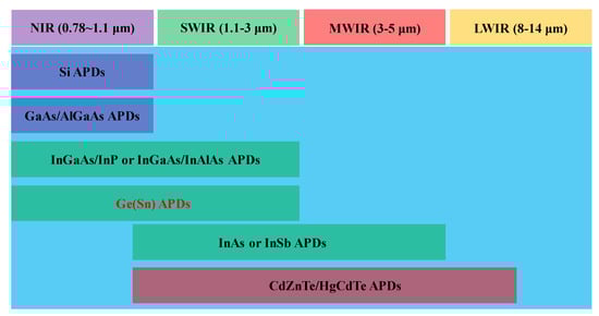
Figure 2.
Typical semiconductor APDs versus infrared waveband.
Currently, there are several types of distance measurement techniques, including time of flight (TOF), triangulation, time of sight (TOS), phase shift, etc. Among all these techniques, the TOF method is one of the most widely used and straight-forward solutions. To keep the budget low, one should choose the common type of lasers, and these lasers should supply high power in short pulses, thus giving the receiver a strong return signal. For the near-IR lasers that operate in the range from 850 nm to 940 nm, they did not meet the requirements of being “eye-safe”. On the other hand, adverse environmental conditions (such as fog, rain, desert dust, humidity, oceanic aerosol, etc.) make the detection extremely challenging due to the severe scattering and absorption effects between the laser and ambient environment. To deal with this problem, the operation wavelength moves towards 1.55 μm (despite the “eye-safe” issue, a wavelength of 1.31 μm might also be available due to less scattering), which is both “eye-safe” and has less scattering [23,24]. Technically, it is therefore raising the spectral region requirements from the detection terminal (SWIR region).
Current APDs technology operating in the SWIR region is based on InGaAs/InP materials, which have several problems, such as expensive fabrication processes, smaller wafer sizes, high afterpulsing effects, long dead-times, high dark count rates (DCRs), low operation temperatures, etc. Group IV materials have the advantages of tunable band structure, larger wafer size, low cost, and compatibility with Si CMOS technology, which are naturally easier to transfer for mass volume production [25,26]. To extend the spectral wavelength range of group IV APDs, tremendous efforts have been made. A significant breakthrough has been achieved in Ge semiconductor material, whose bandgap difference is only 136 meV. Several strategies were proposed to tune the band structure of Ge, including heavy n-type doping, tensile strain engineering, the incorporation of a group IV Sn (Pb) element into Ge, and their combination technique. It has long been verified that GeSn alloys are able to enhance the spectral absorption coefficient at wavelengths of 1.55 μm and 2 μm, indicating that GeSn is also an effective absorber for group IV APD [27,28,29,30].
To the best of our knowledge, there are no review articles about APDs made of both Ge (GeSn) and InGaAs materials [31,32,33,34]. The objective of this review paper is to give researchers a full understanding of recent advancements in materials for APDs and the rapid development towards SWIR for future LiDAR systems. The scaffold of this paper is shown in Figure 3. In Section 2, we focus on the recent research progress for Ge (GeSn) and InGaAs SWIR APDs for mesa and planar geometry, and other novel avalanche device structures. In Section 3, we present the advances of SWIR APDs focal plane arrays (FPAs) and the technology challenges and perspectives.
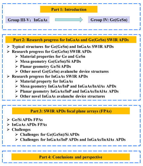
Figure 3.
Outline of this review article.
2. Research Progress for Ge(GeSn) and InGaAs SWIR APDs
2.1. Typical Structures for Ge(GeSn) and InGaAs SWIR APDs
To achieve high-performance APDs, they should have a large multiplication factor (M), a low excess noise factor (F), and a high gain-bandwidth product (GBP). Thus, separation absorption and multiplication (SAM) structures were proposed, in which only light was absorbed in the absorption region and one carrier type was transported into the multiplication region. Thus, M, F, and GBP were considered. In addition, the electric field should be low enough to avoid band-to-band tunneling in the Ge (or GeSn) and InGaAs materials. Figure 4 shows the typical schematic diagram and electric profile of the SAM APDs [35]. For the case of Ge/Si APDs’ separation absorption, researchers usually use the separation absorption, charge, and multiplication (SACM) structure. The schematic diagram for the SACM Ge/Si APD and its electric field distribution is shown in Figure 5 (GeSn is similar to this structure) [36].
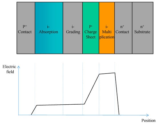
Figure 4.
Typical schematic diagram and electric profile in the SAM APD.
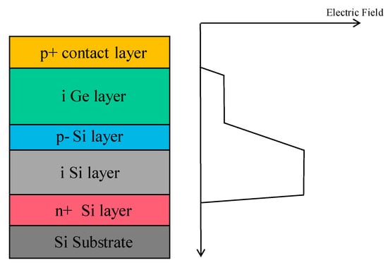
Figure 5.
Schematic diagram and electric field distribution of SACM Ge/Si APD.
For InGaAs/InP APDs, the schematic diagram and its electric field distribution were as follows (Figure 6) [37]. Schematic diagram and electric field distribution of InGaAs/InP APDs were shown in Figure 7 [37].
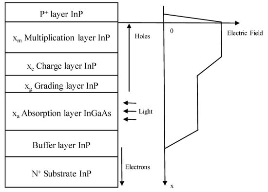
Figure 6.
Schematic diagram and electric field distribution of separate absorption, grading, charge, and multiplication (SAGCM) InGaAs/InP APDs.
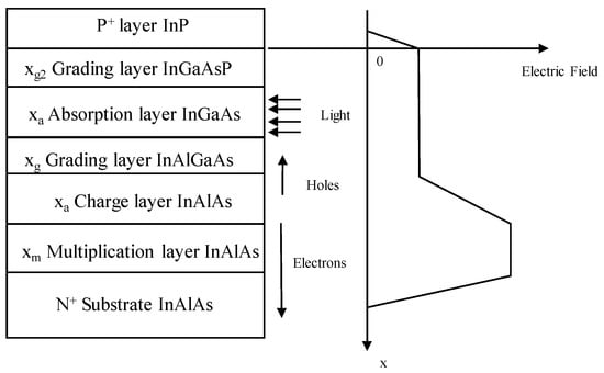
Figure 7.
Schematic diagram of separate absorption, grading, charge, and multiplication (SAGCM) InGaAs/InAlAs APDs and its electric field distribution.
To the best of our knowledge, both InGaAs/InP APDs and InGaAs/InAlAs APDs are commercially available. However, Ge/Si APDs are also a promising technology to achieve high-performance detection due to their low cost and compatibility with the Si CMOS process.
2.2. Research Progress for Ge (GeSn) SWIR APDs
So far, several types of growth techniques, such as MBE [38,39,40,41], magnetron sputtering [42,43], and CVD [44,45], have been used to grow Ge (GeSn) materials. Although Si APD exhibits high performance (high detection efficiency and low dark count probability), its spectral region is limited by the bandgap properties. To extend the operation wavelength, InGaAs or Ge were used as absorbers, and Si was used as a multiplication layer. The reason for using Si as the multiplication region is its low excess noise factor, which is favorable for avalanche breakdown. For the benefits of the Ge absorber, including that Ge was able to grow on large wafer-size Si platforms using CVD technology, it was compatible with traditional CMOS technology, it had good absorption properties with the wavelength cutoff of 1.6 μm at 300 K, it was easily integrated with CMOS circuits, etc. As is shown in Figure 8, both linear mode and Geiger mode Ge/Si APDs were achieved experimentally. To extend the light detection wavelength range, Sn was incorporated into the Ge matrix. Due to the growth technique limitation, only linear mode GeSn APDs were achieved, and GeSn SPADs are still in the simulation stage. Based on the geometry, both mesa-type and planar-type Ge/Si APDs were proposed. However, only mesa-type GeSn APDs were reported, and there is still no experimental demonstration of the planar-type GeSn APDs.
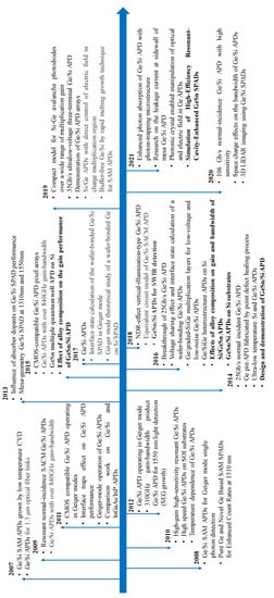
Figure 8.
Research development of Ge(GeSn) APDs.
2.2.1. Material Properties for Ge and GeSn
Different from Si, the band structure of Ge differs from Si conduction band arrangement. The energy bandgap difference between the direct bandgap and indirect bandgap of Ge is only 136 meV, and its band structure can be modulated via N+-type doping engineering, tensile strain engineering, and Sn-based alloy engineering. As noted earlier, Sn is a group IV element, which is a borderline material. Generally, there are two types of tin allotropes (including gray tin and white tin); gray tin (α-Sn) will transfer to white tin (β-Sn) at near room temperature, and their energy difference is extremely small. α-Sn exists in the form of a diamond structure and is more stable. However, β-Sn structure is distorted from the ideal diamond structure. To form the ideal (Si)GeSn alloys, we expect to incorporate diamond structure α-Sn into (Si)Ge crystals, and no phase transformation occurs (white tin). From the band structure of α-Sn, the lowest conduction band and highest valence band all touch the zone center, indicating the band gap of α-Sn is exactly zero (temperature and pressure are not able to change this special nature) [46,47].
To extend the light absorption range of pure Ge, Sn-based alloy engineering was considered the most promising routine, which acts similarly to the tensile strain in Ge and also lowers the direct valley below the indirect valley for tunable band structure (Figure 9). More importantly, direct bandgap GeSn can be used as the efficient light absorption layer for Si-based SWIR detectors, which are fully CMOS-compatible with the large-scale OEICs on the low-cost Si platform. Thus, widespread theoretical research on the crossover of direct bandgap GeSn was conducted (Table 1).
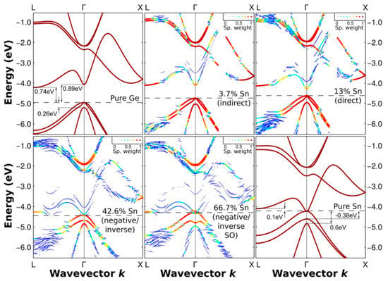
Figure 9.
Band structures of bulk Ge and α-Sn (first and last figures, respectively), GeSn materials with various compositions (3.7%, 13%, 42.6%, and 66.7%). The color and point size denote the Bloch spectral weight, and the points with weights lower than 0.05 are neglected. Reproduced with permission from [46], IOP Publishing, 2017.

Table 1.
Theoretical study on the material properties of direct bandgap GeSn in terms of institution, theoretical methods, and Sn composition.
Table 1.
Theoretical study on the material properties of direct bandgap GeSn in terms of institution, theoretical methods, and Sn composition.
| Year | Institution | Methods | Sn (%) | Ref. |
|---|---|---|---|---|
| 1987 | University of Notre Dame | Tight-binding calculations using virtual-crystal approximation (VCA). | >20 | [48] |
| 1989 | Swiss Federal Institute of Technology | Self-consistent ab initio pseudo-potential calculations in VCA. | 27–74 | [49] |
| 1999 | Michigan Technical University | First-principles calculation in nonlocal density approximation to density functional theory (GGA) with Becke exchange functional with Ferdew-Wang’s correlation functional. | 50 | [50] |
| 2007 | University of Leeds | Charge self-consistent pseudo-potential Xα method. | 17 | [51] |
| 2008 | Fudan University | First-principles fully relativistic band structure method and a more accurate approach that considers core-level volume deformation (VD) potential. | 25, 50, 75 | [52] |
| 2011 | Stanford University | First-principles calculations using density function theory (DFT) with GAA+U. | 3, 6 | [53] |
| 2012 | National University of Singapore | Empirical pseudo-potential method (EPM), 8-band k.p method | 0–20. | [54] |
| 2012 | Shenyang University of Technology | First principles calculations based on norm-conserving pseudo-potentials, density function theory (DFT), and density functional perturbation theory (DFPT). | —— | [55] |
| 2013 | Stanford University | Virtual crystal approximation (VCA) within the framework of the nonlocal empirical pseudo-potential method (NL-EPM). | 0–20, 7 | [56] |
| 2014 | ETH Zurich | Empirical pseudopotential method (EPM) along with virtual crystal approximation (VCA). | 0–20 | [57] |
| 2015 | Chinese Academy of Science, Institute of Semiconductor | First-principle calculations based on DFT are performed using the Vienna ab initio simulation package (VASP) code. To correct the underestimation of the bandgap, the GGA+U approach with Perdew–Burke–Ernzerhof (PBE) is employed to describe the electron exchange and correlation. | 0–20, 8.5 | [58] |
| 2017 | Wroclaw University of Science and Technology | First-principle calculations based on DFT along with Tran and Blaha MBJLDA functions. All calculations have been performed with the all-electron full potential WIEN2k code, which has recently been proven to be one of the most accurate DFT codes. | 3.7–66.7 | [46] |
| 2018 | University College Cork | First-principle calculations based on DFT, including Heyd Scuseri Ernzerhof (HSE) hybrid functions, using the Vienna Ab initio Simulation Package (VASP). | 6.25 | [59] |
| 2019 | National Chiao Tung University | Nonlocal empirical pseudopotential method (EPM) with modified virtual crystal approximation (VCA), 8-band k.p model. | 0–15, 7.1 | [60] |
| 2019 | Nanyang Technological University | Empirical tight binding and ab initio methods, full-zone 30-band k.p model. | 0–30, 7.25 | [61] |
| 2020 | George Washington Unviersity | Combining statistical sampling based on the Monte Carlo method and density functional theory (DFT) calculation using the Vienna Ab initio Simulation Package (VASP) based on the projector augmented wave method. | 25, 8 | [62] |
| 2020 | Tiangong University | First-principle calculation via the sX-LDA method, using the Cambridge Sequential Total Energy Package (CASTEP) code based on the DFT, The norm-conserving pseudopotentials (NCPP) are used to describe the interactions between the electrons and ionic cores. | 0–30, 6.25 | [63] |
| 2021 | University College Cork | First-principle calculations based on Kohn–Sham DFT, Structural relaxations are carried out in the local density approximation (LDA), and electronic band structures are calculated using the Tran–Blaha modified Becke–Johnson (TB-mBJ) meta-generalized gradient approximation (meta-GGA) exchange-correlation potential in order to overcome the band gap underestimation typical of the LDA in the Kohn–Sham formalism. | 0–100, 5, 11, 25 | [64] |
Many theoretical research works have been conducted to evaluate the material properties of GeSn, especially for the band structure of direct bandgap GeSn. Among all these theory methods, density functional theory (DFT)-based first-principles calculations have been shown to yield an overall good agreement with experimentally observed GeSn band gaps. However, there is still a lack of an in-depth study on the point defect behavior on the GeSn material properties, whether Sn vacancies or Ge vacancies. The existence of a point defect will affect the material properties, thus increasing the leakage current and reducing the quantum efficiency of the GeSn photodetectors. To determine the absorption coefficient of GeSn with various compositions, extensive spectroscopic ellipsometry measurements had been performed for all the samples (Figure 10). GeSn layers were grown on Ge (100) substrate, which suffers from compressive strain.
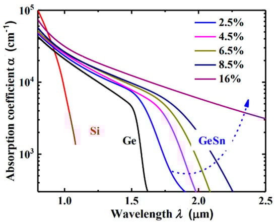
Figure 10.
Absorption coefficient of compressive GeSn on Ge with various Sn compositions ranging from 2.5 % to 16 %. Reproduced from [65], open access by NUS Library, 2019.
In the past decade, tremendous efforts had been made on the GeSn photo detection. With a very small incorporation (2%) of Sn into Ge, the absorption coefficient for GeSn is several times higher than that of bulk Ge (Figure 10). In the meantime, the cutoff wavelength for the Ge0.98Sn0.02 photodetector is sufficient to fully cover all the telecom windows (from O-band to U-band: 1260 nm to 1675 nm) [27]. By incorporating more Sn atoms into Ge, wavelength coverage can be further extended to longer wavelengths. For SWIR detection, incorporation of 10–11% of Sn is necessary to cover the entire SWIR wave band, which is extremely suitable for the thick GeSn layer due to the strain relaxation growth mechanism [28]. Experimental research had demonstrated that the cutoff wavelength was extended to 3.7 μm with more than 20% Sn incorporation [29].
2.2.2. Mesa Geometry Ge(GeSn)/Si APDs
At the initial research stage for Ge(GeSn) APDs, mesa structures are generally acknowledged due to their reproducibility and fabrication simplicity.
Y. Kang et al. [66] demonstrated the first mesa-type Ge/Si APDs for 1.31 μm light detection, which are based on the conventional separate absorption charge and multiplication (SACM) structure (Figure 11). Ge and Si are designed as the absorber and multiplier, respectively. To obtain this structure, a commercial CVD chamber was utilized to grow the Si multiplication layer and Ge absorption layer. After the growth, circular mesas were wet-etched. To reduce the threading dislocation densities (TDDs) originating from the Si/Ge interface, an annealing process was carried out in the temperature range of 800 °C–900 °C. Si3N4 film was deposited as passivation and planarization, which is also used as an anti-reflection coating. The characterization results exhibit a responsivity of 0.54 A/W with the 1.31 μm incident light, dark current densities as low as 237 mA/cm2 at 90% breakdown voltage, a breakdown voltage thermal coefficient of 0.05%/°C, and a 3dB-bandwidth of 10 GHz.

Figure 11.
Schematic cross-section of Ge/Si SACM APD.
Zhiwen Lu et al. [67] demonstrated the first relatively complete single photon counting results for Geiger-mode-operated Ge/Si APD. The thicknesses of the Ge absorption layer and Si multiplication layer are 1 μm and 0.5 μm, respectively (Figure 12). The charger layer is p-type doped (1.52 × 1017 cm−3) with a thickness of 0.1 μm. Owing to the large lattice mismatch between the p-Si charger layer and the i-Ge absorption layer (4%), considerable traps were generated in the interface, leading to the higher dark current. To characterize the single photon detection efficiency (SPDE) and dark count rate (DCR), a 1.31 μm pulsed laser was employed as the light source (the optical pulse width and pulse repetition rate are 50 ps and 100 kHz, respectively). Experimental results show that an SPDE of 14% and a DCR of 108 Hz were achieved. However, DCR is very high, and the device does not have enough time to recover its bias lever before other DCs are triggered, which will cause the underestimation of DCR at a certain bias.
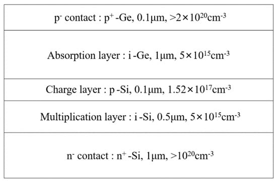
Figure 12.
Layer structure for separate-absorption-charge-multiplication (SACM) Ge/Si APD.
To improve the device’s performance, several modifications had been made to the above-mentioned APD structures (Figure 13). First, the i-Si multiplication region was increased to 1.0 μm, which will raise the voltage difference between the avalanche breakdown voltage and punch-through voltage. Then, the doping concentration for the p-Si charger layer was designed in the range of 1 × 1017cm−3 to 5 × 1017cm−3. As punch-through voltage depends merely on the doping concentration of the charger layer, one can alter the voltage difference by changing the doping level. Especially at low temperatures, small voltage differences will remarkably lower the SPDE for APD at 1.31 μm and 1.55 μm. To characterize the low-temperature performance, APD devices were mounted in the liquid nitrogen (LN2)-cooled cryostat. Both pulsed semiconductor lasers were employed to evaluate the SPDE at wavelengths of 1.31 μm and 1.55 μm [68]. With the illumination of a 1.31 μm pulsed laser, low temperature (100 K) SPDE is approximately 4% at 10% excess bias. However, low temperature SPDE (at the wavelength of 1.55 μm) was measured to be 0.15% at 6% excess bias, which is mainly due to the reduced absorption edge for Ge at low temperatures. At the temperature of 150 K, DCRs of 106–107 Hz were clearly observed, which is still several orders of magnitude higher than InGaAs/InP planar SPADs (102–103 Hz). These high DCRs were attributed to the high dark currents due to the high defect level in the Ge absorption layer and narrow bandgap of Ge. Moreover, sidewall surface recombination was also responsible for the high dark current.
Figure 13.
Cross-section schematic of Ge/Si mesa type APD structures (Si3N4 was utilized for passivation and planarization).
Different from previously reported mesa-type Ge/Si APD, Ning Duan et al. [69] adopted selective epitaxial growth (SEG) to form the Ge absorption layer and the Si multiplication layer. On the one hand, SEG Ge growth was able to reduce the device processing complexity; on the other hand, it can also prevent the mesa edge breakdown. Growth procedures for SACM Ge/Si APD are as follows: (I) high-resistivity (100) SOI substrates with 220 nm Si layer and 2000 nm buried oxide; (II) bottom n-type Si contact formation: As ion implantation; (III) SEG growth of 700 nm Si multiplication layer at 600 °C; (IV) p-type charge layer formation: implanting B into the as-grown Si; (V) SEG growth of 1000 nm Ge absorption layer: including 50 nm SiGe buffer, 50 nm Ge seed layer growth at 350 °C, and high temperature Ge growth at 550 °C (Figure 14). With proper design, the responsivity and gain-bandwidth of the SEG-grown mesa-type Ge/Si APD at 1550 nm are 12 A/W and 310 GHz, respectively. One important point for selective growth integration is pattern dependency. The growth rate (and composition) can be altered due to chip layout. This means that the uniformity issue may arise over the process wafer and has to be tackled [70,71,72,73].

Figure 14.
TEM images of (a) mesa-type Ge/Si APD by SEG growth; (b) total layer thickness. Reproduced from [69], OSA Publishing, open access, 2012.
Although Ge was used as the absorber to realize Ge/Si APDs, the absorption coefficient of Ge becomes very low at wavelengths beyond 1.6 μm, which makes Ge/Si APDs unsuitable for imaging in the wavelength range from 1.6–3 μm. With the incorporation of Sn into Ge, an enhanced absorption coefficient was observed, and its absorption range was also extended beyond 1.6 μm. Due to its enhanced absorption range and absorption coefficient, GeSn was designed as the absorber for SACM GeSn/Si APD (Figure 15). To characterize the GeSn/Si APD with a mesa size of 30 μm, incident laser wavelength and laser power were employed as 1600–1630 nm and 0.5 mW, respectively. Figure 16 shows the I-Vbias characteristics and responsiveness for the GeSn/Si APD. It is clearly observed that the I-Vbias curves stay almost the same with various incident laser wavelengths (1600–1630 nm). However, responsivity increases significantly with the bias voltage of −9.7 V owing to the internal gain (Figure 16b).
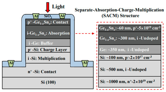
Figure 15.
Schematic for first demonstration of SACM GeSn APD with Sn composition up to 5%. Reproduced with permission from [74], IEEE, 2014.

Figure 16.
(a) I-Vbias characteristics of GeSn/Si APD under the illumination of 1600 nm, 1610 nm, 1620 nm, and 1630 nm incident laser light; (b) relationship between responsivity and wavelength at −5 V and −9.7 V. Reproduced with permission from [74], IEEE, 2014.
Different from the SACM APD with bulk GeSn absorber, the GeSn/Ge MQWs absorber has the following advantages: (1) increase the critical thickness; (2) MQWs’ structure is favorable for light absorption, emission, and modulation, which is also helpful for future optoelectronic integrated circuits (OEICs). Thus, photons are absorbed in the GeSn/Ge MQWs structure and electrons are generated; charge multiplication occurs in the intrinsic Si layer (Figure 17). With the 10% Sn incorporation into GeSn/Ge MQWs, the wavelength cutoff was further extended above 2 μm.
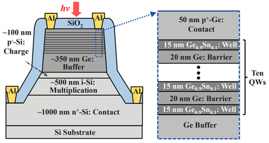
Figure 17.
Cross-sectional schematic of GeSn/Ge MQWs APD with SACM structure. Reproduced with permission from [75], IEEE, 2015.
Figure 18 illustrates the wavelength-dependence responsivity of GeSn/Ge MQWs APD. To carry out the optical response measurement, two types of light sources (including tunable lasers and distributed feedback laser diodes) were used. At each incident wavelength (1510 nm, 1630 nm, 1742 nm, 1877 nm, and 2003 nm), GeSn/Ge MQWs APDs were biased at −5 V, −9 V, and −10 V. At the wavelength of 2003 nm, responsivities for GeSn/Ge MQWs’ APD biased at the voltages of −5 V and −10 V are 0.029 and 0.33 A/W, indicating avalanche multiplication occurs and peak avalanche gain is evaluated to be ~15 when biased at -10 V. In addition, the thermal coefficient of the breakdown voltage is calculated to be 0.05% °C−1, which is smaller than InGaAs/InP APDs, suggesting GeSn/Ge MQWs APD is less dependent on the temperature.

Figure 18.
Optical responsivity for GeSn/Ge MQWs APD is biased at different voltages. Reproduced with permission from [75], IEEE, 2015.
Despite the rapid development of GeSn photodetectors, GeSn SPADs have not been demonstrated yet. To achieve high SPDE, low DCR, and high operation temperatures in GeSn SPADs, Qimiao Chen et al. [76] proposed resonant-cavity-enhanced (RCE) GeSn SPADs operating at 1.55 μm and 2 μm, respectively (Figure 19). Major design considerations were as follows: (I) To decrease the DCR, the SACM structure was employed so as to avoid the band-to-band tunneling in the GeSn absorption layer; (II) photon absorption probability can be greatly improved by sandwiching the GeSn absorber and the Si multiplication layer with vertical cavity, thus increasing the SPDE (Sn compositions for the 1.55 μm and 2 μm light absorbers were 3% and 10%, respectively); (III) the electric field intensity in the Si multiplication layer is the highest in the whole layer structure, and the electric field distribution should also be uniform; (IV) the electric field in the GeSn absorber needs to be moderate, thus photon-generated electrons are able to drift into the high-electric field Si multiplication layer and make the contribution to the SPDE; (V) high background doping concentrations and high defects in the GeSn absorber cause a negative effect on SPADs, which is important for high-performance SPADs. With proper design, SPDE for GeSn SPADs was predicted to be 80% at the wavelength of 1.55 μm, which features RCE GeSn SPADs are a promising candidate for high efficiency single photon detection in the SWIR region.
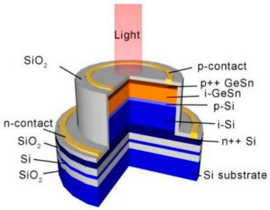
Figure 19.
Proposed RCE GeSn SPAD structure with GeSn absorber and Si multiplication layer. Reproduced with permission from [76], IEEE, 2021.
2.2.3. Planar Geometry Ge/Si APDs
As researchers mentioned, planar geometry avoids the sidewall contribution to the dark current and can further decrease the DCRs; thus, Ge APD has the potential to operate at higher temperatures, and SPDE might also be significantly improved. To examine the electric field distribution in the whole device structure, a TCAD simulation study for the planar geometry Ge/Si APDs was performed. Figure 20 shows the optimal electric field distribution due to the following considerations: (I) the electric field in the i-Ge absorber is low at breakdown, so photo-generated electrons can drift to the i-Si multiplication layer more efficiently; (II) the electric field in the i-Si multiplication layer is high, which is helpful for the impact ionization of electrons; (III) the electric field was confined into the center of the Ge SPAD, preventing the sidewall effects.

Figure 20.
Electric field distribution for Ge/Si SPAD at 5% excess bias above the breakdown (the thickness of the Ge absorber is 1 μm). Reproduced from [77], ROS Theses Repository, open access, 2019.
In 2019, Peter Vines et al. [77] demonstrated a new generation of planar Ge/Si SPAD for SWIR operation (Figure 21). Compared with the mesa-type, planar geometry was able to avoid the sidewall recombination effect, which is helpful for DCR reduction. Before the 1.3 μm laser radiation, SPADs were cooled down to a low temperature for SPDE, DCR, and jitter measurements. At 100 K, SPDE was improved to 26%, which is several times higher than previous reported mesa-type SPADs (4%). Moreover, DCR was three orders of magnitude lower than mesa-type results. After increasing the temperature to 125 K, SPDE for planar geometry Ge SPADs (38%) is comparable to the commercial InGaAs/InP SPADs. Based on Beer–Lambert’s law, low temperature (125 K) SPDE can be further improved to be 55% with a 2 μm Ge absorption layer. The jitter full width at half maximum (FWHM) is 310 ps, which can be optimized by decreasing the device diameter. To check the afterpulsing mechanism for planar geometry Ge/Si SPAD, afterpulsing probability was evaluated at a temperature of 125 K, which features 20% of the InGaAs/InP SPAD (Figure 22). A similar trend was also observed at 150 K. Moreover, the noise equivalent power (NEP) of 1.9 × 10⁻¹⁶ W/Hz1/2 at T = 78 K is a 50-fold improvement on previously reported Ge-on-Si SPADs. From the planar Ge/Si SPAD results, smaller diameter devices with low TDD and thick Ge absorption layers will allow the device to work at higher temperatures (high SPDE at the wavelength of 1.55 μm), lower DCRs, and lower afterpulsing probabilities.
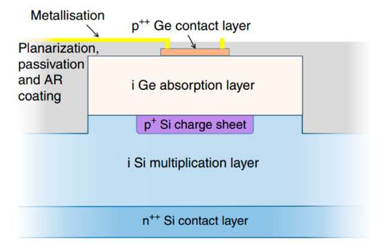
Figure 21.
Cross-section diagram of a planar Ge/Si SPAD structure with an i-Ge absorption layer, a p+-Si charge layer, and a i-Si multiplication layer. Reproduced from [77,78], ROS Theses Repository, and Springer Nature, open access, 2019.
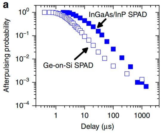
Figure 22.
Comparison of afterpulsing probabilities vs. gate delay time between planar Ge/Si SPAD (100 μm diameter) with commercial InGaAs/InP SPAD (25 μm diameter). Reproduced from [78], Springer Nature, open access, 2019.
To further decrease the DCRs of 100 μm diameter planar geometry for Ge/Si SPAD, device diameters were fabricated to be 26 μm and 50 μm. Device performance for the Ge/Si SPAD with different diameters was summarized as follows: in terms of temperature, SPDE, DCRs, Jitter, and NEP (Table 2). It was found that an extremely low DCR was achieved for the 26 μm diameter detector, indicating excellent sensitivity for planar geometry Ge/Si SPAD. Although the maximum SPDEs of the 26 μm and 50 μm devices were 10% lower than those of the 100 μm device, jitter and the NEP for the 26 μm device were 157 ± 10 ps and 9.8 × 10⁻¹⁷ WHz−1/2, respectively. The 26 μm diameter device shows record-low NEP, which suggests planar geometry has the potential to achieve low-cost and high-speed Ge/Si SPAD arrays in the SWIR spectral region. Compared with the commercial InGaAs/InP SPAD, the Ge/Si SPAD features lower DCRs and shorter data acquisition times.
Table 2.
Summarized device performance for planar geometry Ge/Si SPAD at 1.31 μm [77,78,79].
To further improve the SPDE for planar geometry Ge/Si SPAD, it is important to evaluate the effect of Ge absorber thickness. Generally, thicker absorbers contribute to better absorption and more photogenerated carriers. Based on Lambert–Beer’s law, less than 50% of 1.31 μm light is absorbed in the 1 μm Ge absorber. To improve the absorption efficiency, it is essential to increase the Ge absorber thickness. As is estimated by the researchers, 75% and 88% of 1.31 μm light are absorbed within 2 μm and 3 μm Ge absorbers, respectively.
From Figure 23 and Figure 24, electric field distributions for Ge/Si SPAD with 2 μm and 3 μm thick absorbers were clearly observed. Compared with Ge/Si SPAD with a 1 μm absorber, the electric field near the sidewall is higher for the 3 μm absorber, indicating that the dimensions of Ge/Si SPAD still require further design optimization.
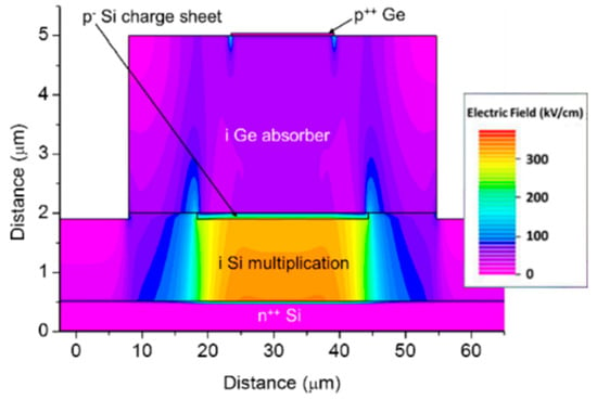
Figure 23.
Electric field distribution for Ge/Si SPAD at 5% excess bias above the breakdown (the thickness of the Ge absorber is 2 μm). Reproduced from [77], ROS Theses Repository, open access, 2019.
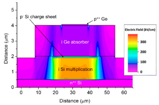
Figure 24.
Electric field distribution for Ge/Si SPAD at 5% excess bias above the breakdown (the thickness of the Ge absorber is 3 μm). Reproduced from [78], Springer Nature, open access, 2019.
2.2.4. Other Novel Ge(GeSn) Avalanche Device Structures
The emerging two-dimensional (2D) layered materials have proven to be a promising candidate for photodetection due to their excellent properties, including ultrathin structure, thickness-dependent band structure, dangling bond immunity, and high light absorption. Another type of candidate material for photodetectors could be 2D crystals, especially graphene. The disadvantage of such detectors is their low response time [80,81].
Efforts have been made to develop 2D/Ge van der Waals heterostructures for broadband photodetection (Figure 25). Recently, Yuan et al. [82] demonstrated a novel avalanche photodetector based on p-Ge/n-MoS2 van der Waals heterojunction, which shows that the heterojunction with an Ag electrode exhibits a better rectification effect and lower breakdown voltage than the device with an Au electrode. The device shows a maximum responsivity of 170 and 4 A/W under 532 and 1550 nm illumination, respectively. The device with high optical detection performance under both visible and infrared illumination provides a new, novel, and promising path for broadband photodetection.

Figure 25.
Schematic diagram of MoS2/Ge heterojunction with (a) Ag electrode, (b) Au electrode, and (c) optical image of MoS2/Ge heterojunction. Reproduced from [82], Optica Publishing, open access, 2022.
The 2D/3D heterojunctions can also be appropriately applied to junction field-effect transistors (JFETs), which operate by changing the depletion region of the p-n junction. Gate-tunable and photoresponsivity behaviors of JFETs based on 2D/3D heterojunctions are demonstrated in ref [76]. The JFET shows a low sub-threshold swing of ≈88 mV/dec and a high on/off current ratio of ≈105. By modulating the gate voltage, the device can reach a peak positive responsivity of 66 A/W under visible illumination at 532 nm. In contrast, the device exhibits a modifiable negative responsivity behavior under IR illumination at 1550 nm due to the combined effect of different polarity currents in MoS2 and Ge (Figure 26) [83]. These results provide a new strategy for the development of novel 2D/3D optoelectronic heterostructures that have good potential as multifunctional optoelectronic units.

Figure 26.
Schematic diagram structure of MoS2/Ge heterostructure JFETs.
For many years, APDs were considered an attractive option for digital fiber-optic communications. However, induced impact ionization requires high operating voltages (typically greater than 8 V) and can introduce considerable noise, which hinders its practicality. Another option is to use phototransistors (PTs) to provide high responsivity and bandwidth while biasing at low voltages. Some group III–V compound alloy materials, such as (GaAl)As/GaAs and InP/InGaAs, have been widely used to fabricate such phototransistors. Recently, the development of group IV-based semiconductor materials has also started to receive increasing attention, and active efforts are being made to realize high-speed PTs [84]. Ang et al. [85] fabricated floating-base germanium phototransistors with the N/P/i-Ge/N configurations by using a low-temperature selective Ge epitaxy process (Figure 27). The current gain induced by transistor action allows the device to achieve large photocurrent and optical response enhancement at a low operating bias compared to conventional p-i-n Ge photodetectors. An impressive 2.0 A/W responsivity is obtained at 1.55 μm optical illumination at −1.0 V.

Figure 27.
SEM image and schematical diagram of a Ge phototransistor.
Photonic devices using group IV semiconductors on Si platforms have been of great interest for decades due to the indirect nature of the band gap of Si materials. However, there is a large lattice mismatch between the two materials, which makes the growth of Ge/GeSn on Si substrates a problem. In the last 15 years, the situation has improved dramatically with the successful growth of GeSn and the discovery of practical chemical vapor deposition (CVD) routes. The formation of high-quality GeSn films and GeSiSn alloys directly on Si substrates can be achieved. The addition of a few percent of substitutional Sn to Ge can effectively narrow the direct band gap of Ge and extend the wavelength range for absorption to more than 1550 nm. Ordinary p-i-n PDs have no internal optical gain, and APDs with internal optical gain have the disadvantages of high operating voltage and high noise. GeSn phototransistors (PTs) are considered a useful alternative to normal PDs because they have internal optical gain while operating at low voltage and without excess noise. In 2015, the performance of a front-side illuminated Ge–GeSn–GeSn hetero phototransistor grown on a Si platform was demonstrated [85]. The terminal currents, current gain, optical gain, and responsivity of the HPT at 1.55 µm were calculated. People find that the values are comparable with those in InGaAs/InP systems, and the values for GeSn-based HPTs are even higher for lower values of base doping and base width. The proposed structure can be grown on a silicon platform, which allows it to be used as a viable alternative to InGaAs-based detectors in the C and L-band for fiber optic communications (Figure 28).
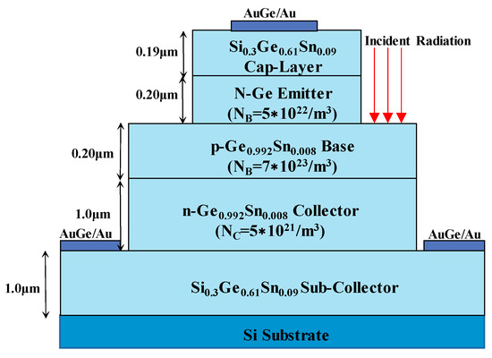
Figure 28.
Schematic diagram for a front-side illuminated Ge–GeSn–GeSn hetero phototransistor.
2.3. Research Progress for InGaAs SWIR APDs
Up until now, there have mainly been two techniques to grow the InGaAs/InP APDs, including molecular beam epitaxy (MBE) and metal organic chemical vapor deposition (MOCVD). Different from MBE, MOCVD can achieve a high growth rate at a lower vacuum, which is more suitable for industrial large-scale growth. Compared with the Ge/Si APDs, In0.53Ga0.47As/InP APDs possess superior performances in the SWIR range (0.9–1.7 μm), which covers the 1550nm eye-safe LiDAR (Figure 29). As one of the most promising eye-safe APDs, SAGCM structure InGaAs/InP APDs were generally acknowledged. Due to the small lattice mismatch between In0.53Ga0.47As and InP (0.0424%), In0.53Ga0.47As and InP were employed as the absorption region and multiplication region, respectively. To avoid carrier accumulation at the heterostructure interface and alleviate the energy discontinuity between the In0.53Ga0.47As and InP interfaces, the InGaAsP grading layer was introduced. Due to the lattice match between InGaAs and InAlAs, InAlAs were also utilized as the multiplication region for the InGaAs/InAlAs APDs, which feature better higher gain at the low dark current level. Therefore, InAlAs is gradually replacing the InP multiplication region owing to its superior ionization coefficients, which leads to reduced excess noise. At the same time, InAlAs has a wider bandgap, which is also helpful for the reduction of tunneling current.
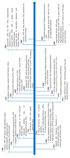
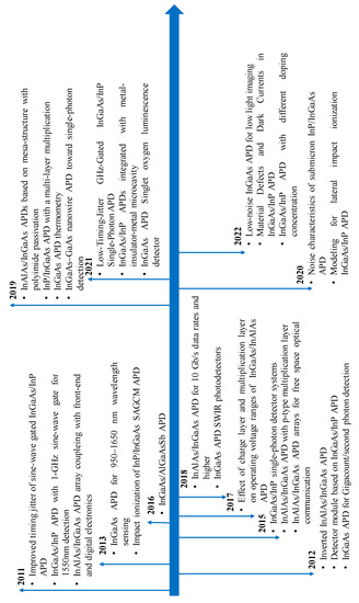
Figure 29.
Research development of InGaAs APDs.
2.3.1. Material Property for InGaAs
The optical and electronic properties of ternary InGaAs can be aligned by varying the ratio of InAs and GaAs. The cutoff wavelength of ternary In0.53Ga0.37As is approximately 1.7 μm, which is well lattice matched with the InP substrate, which has been widely used for SWIR detection. To extend the wavelength cutoff, more indium should be introduced, but this leads to a larger mismatch with InP, thereby generating defects and degrading the crystal quality. Accordingly, In0.53Ga0.37As is the superior choice to form the high-quality SWIR absorber, especially for the 1550 nm eye-safe LiDAR application. Compared with the Ge absorber, In0.53Ga0.37As has superior absorption characteristics at 1550 nm over Ge (Figure 30). To this point, InGaAs APDs are more suitable for 1550 nm eye-safe light detection than Ge/Si APDs [86]. It is highly expected that GeSn/Si APDs should be a cost-effective routine to compete with the InGaAs APDs for this application. However, research for the GeSn/Si APDs is still in the preliminary stages, which makes the InGaAs APDs more competitive in the market at the present.
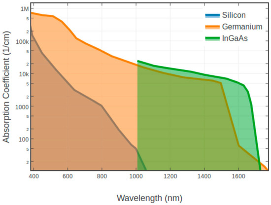
Figure 30.
Comparison absorption characteristics of Si, Ge, and InGaAs. Reproduced from [86], open access by White Rose eTheses Online, 2020.
2.3.2. Mesa Geometry InGaAs/InP and InGaAs/InAlAs APDs
P.Kleinow et al. [87] have grown the InGaAs/InAlAs SAGCM structure on an n+-InP substrate with a combination of a p-type grading layer and charge layer by the MBE system. It had been confirmed that the doping level in the charge layer affects the punch-through voltage (Vpt), break voltage (Vb), and multiplication (M) gain performance. Therefore, special consideration should be given to compromise both the Vpt and the Vb when designing the charge doping level. Despite the charge doping level, p-type doping for the grading layer will reduce the conduction-band barrier between the absorber and multiplication region. Based on the above-mentioned considerations, two designs were proposed. In the first design, it contains a 50 nm undoped InAlGaAs grading layer followed by a 150 nm InAlAs charge layer; in another design, there is also p-type doping in the InAlGaAs grading layer. The main difference between these two designs is the conduction-band barrier height, which is considerably reduced in the second design. Thus, the punch-through voltage was lowered from 10 V (first design) to 8.5 V (second design) (Figure 31). The improved design features a lower dark current density of 1.7 × 10⁻⁴A/cm2 at 20 V bias voltage (Figure 32).
Figure 31.
Schematic diagram of InGaAs/Inyalas SAGCM APDs with calculated band-edge profile.
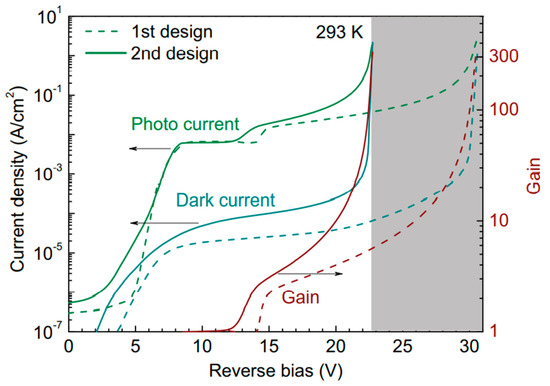
Figure 32.
Dark- and photo-current characteristics (left axis) and multiplication gain (right axis) of different charge-layer designs. Reproduced with permission from [87], WILEY-VCH, 2016.
Jae-Sik Sim et al. [88] designed and fabricated the mesa geometry front-side illuminated InGaAs/InAlAs SAGCM APDs (Figure 33). Under the 1550 nm laser illumination, Vph and Vbr were 10 V and 33 V, respectively. Responsivity was evaluated to be 0.8 A/W@1550 nm, and low dark current (2 × 10⁻⁶cm−2) was observed at the multiplication gain of 10.
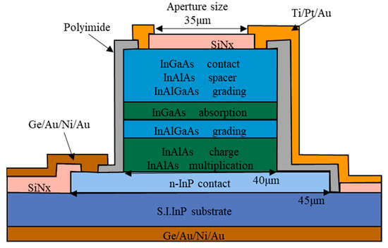
Figure 33.
Cross-sectional diagram and top view image for the mesa geometry front-side illuminated InGaAs/InAlAs SAGCM APDs.
Junqin Zhang et al. [89] investigated the surface leakage current mechanism for the InGaAs/InAlAs SAGCM APDs with various mesas. A typical cross-sectional diagram for InGaAs/InAlAs SAGCM APDs with double-mesas, triple mesas, and multi-mesas were demonstrated in Figure 34. For the double-mesa structure, mesa 1 is for the P-type InP contact layer, P-type InP charge layer, I-InP multiplication layer, N-type charge layer, N-InGaAsP grading layer, and I-InGaAs absorption layer. However, mesa 2 is only for the N-InP contact layer (Figure 34a). For the device structure with triple mesas, mesa 1 and mesa 3 are for the P+-InP contact layer and the N-InP contact layer, respectively. Mesa 2 is for the other parts of the APDs, which include the P-type InP charge layer, the I-InP multiplication layer, the N-type charge layer, the N-InGaAsP grading layer, and the I-InGaAs absorption layer (Figure 34b). In the multi-mesa APD, there are four mesas, mesa 1 and mesa 4 are for the P+-InP contact layer and the N-InP contact layer, respectively. Mesa 2 is for the P-InP charge layer and mesa 3 is for the I-InP multiplication layer, N-InP charge layer, N-InGaAsP grading layer, and I-InGaAs absorption layer (Figure 34c). Finally, they concluded that the main reasons for the generation of sidewall leakage current in the mesa type APDs are as follows: (I) surface charges in the InP multiplication layer, (II) surface recombination centers in the InGaAs absorption layer, (III) intrinsic semiconductor defects. It is found that sidewall leakage current was affected by the mesa geometry, suggesting that multi-mesa APD has been lowest sidewall leakage current level.
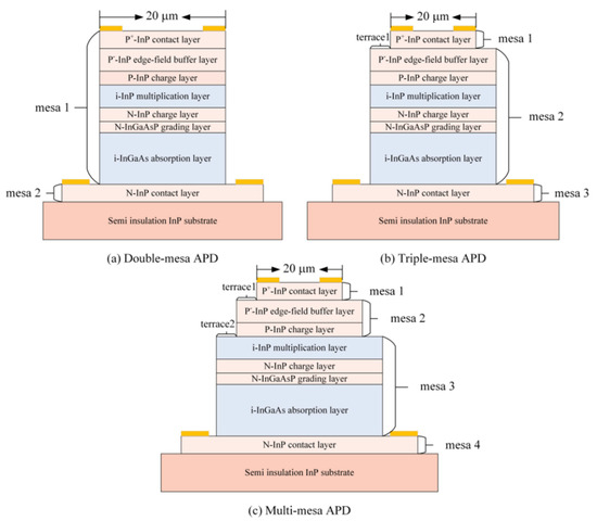
Figure 34.
Cross-sectional diagram for the mesa geometry of InGaAs/InAlAs SAGCM APDs with different mesa. Reproduced from [89], AIP Publishing, open access, 2022.
For the traditional InGaAs/InP SAGCM APD structure, the dark current is higher due to the inherent material defects, which contribute to the lower signal-to-noise ratio (SNR). To solve this problem, reducing mesa the size is an effective method, but it comes at the expense of the optical response. Figure 35 shows the schematic diagram of the InGaAs/InP APD with MIM microcavity, MIM microcavity is directly fabricated on the APD, which includes a top Au grating layer, a middle SiO2 insulator, and a bottom Au double slit layer [90]. The main innovation for this structure is that the MIM microcavity can collimate and focus the incident light and have a higher optical transmittance, which makes it able to achieve the lower dark count rates by reducing the APD size but without sacrificing the optical response and quantum efficiency. Compared with the traditional APD, the SNR of the MIM-APD is twice that of the traditional one, and the 3 dB bandwidth is increased by 49%.
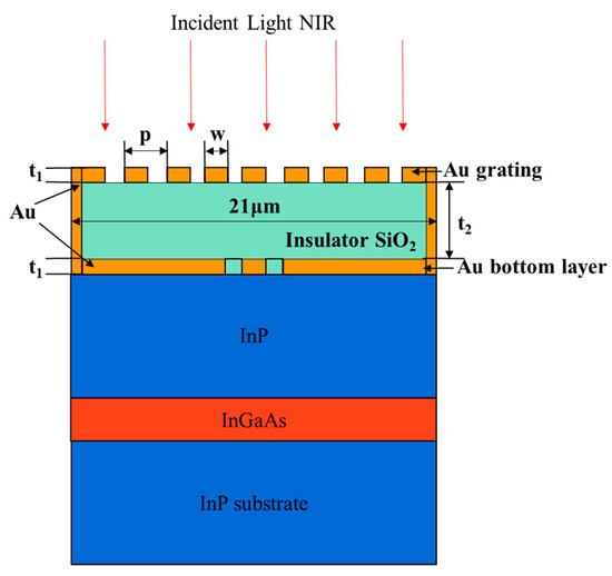
Figure 35.
Schematic diagram of InGaAs/InP APDs with metal-insulator-metal (MIM) optical microcavity and cross-sectional of MIM structure.
2.3.3. Planar Geometry InGaAs/InP and InGaAs/InAlAs APDs
Nowadays, the planar geometry is the mainstream for InGaAs/InP-based SAGCM APDs in commercial products owing to its superior surface leakage current suppression efficiency compared to the mesa geometry. Generally, a high-field p-n junction is required to form the planar geometry of InGaAs APDs, which is achieved by thermal diffusion and/or ion implantation. Since this process is critical for the multiplication region, charge region, and absorption region. After the diffusion process, the p+- region is not an ideal rectangle structure but a circle geometry, which will cause unwanted problems. Hence, a floating guard ring (FGR) structure is used to overcome these problems. To reach a higher surface electric field, p-n junctions require FGR structures (such as single FGRs, double FGRs, deep FGRs, etc.), which will improve the parasitic capacitance and increase the process complexity. Especially for the smaller size APDs, size and location of the FGRs play an important role in the device’s operation.
Zilu Guo et al. [91] grew the InGaAs/InP SAGCM structure on an InP substrate by the MBE system (Figure 36), and deep low-temperature PL spectra were employed to clarify the effect of the material point defect on the dark current of the APDs. From the PL result, there is deep energy level defect in the InGaAs absorption region, which is most likely produced by the point defect from the MBE growth procedure. Then, planar InGaAs/InP APD is fabricated by the Zn diffusion method and guard-ring process, and the intrinsic InP region below the Zn diffusion region is regarded as the multiplication region. Under 20 nW of 1550 nm light illumination, I–V and gain characteristics show that punch-through voltage (Vpt) and breakdown voltage (Vb) are 16 V and 44 V, respectively (Figure 37). In the case where APDs operate in a range from 16 V to 95% of the breakdown voltage, the photo current starts to increase from 3.47 × 10⁻⁸ to 1.93 × 10⁻⁷ A, and the dark current also increases with the reverse voltage (3.89 × 10⁻¹⁰ to 1.09 × 10⁻⁸ A). It was also found that the multiplication gain for the dark current is higher than that of the photo current with the increased electric field, which is mainly due to the material defects. It was also confirmed by the theoretical simulation results.
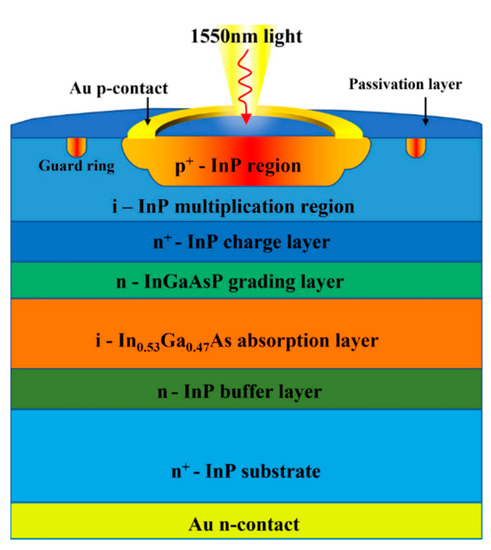
Figure 36.
Schematic illustration for InGaAs/InAlAs SAGCM APDs. Reproduced with permission from [91], IEEE, 2022.
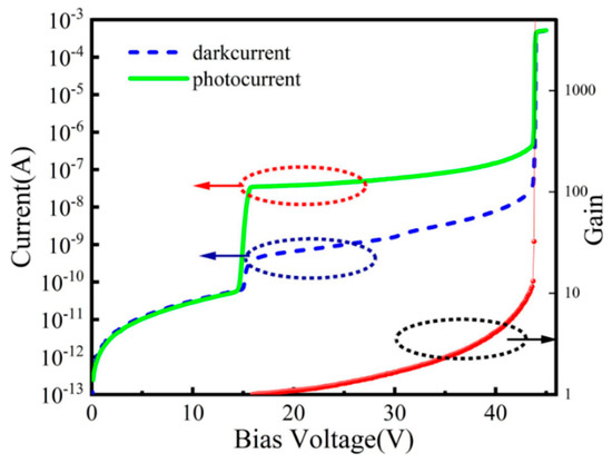
Figure 37.
I-V and gain characteristics of the InGaAs/InP SAGCM structure. Reproduced with permission from [91], IEEE, 2022.
B. F. Levine et al. [92] reported a novel backside-illuminated InGaAs/InAlAs APD with a planar buried multiplication region, which is shown in Figure 38. Compared with other standard APDs, this structure has several advantages: (I) both InAlAs multiplication region and the InAlAs charge region were in-situ doped in the growth chamber, (II) the fabrication process was greatly simplified, (III) there was good wafer uniformity and high reproducibility, etc. Experimental result shows that GBP for this structure is as high as 150 GHz.
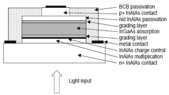
Figure 38.
Schematic illustration for the backside illuminated InGaAs/InAlAs SAGCM APDs. Reproduced with permission from [92], IEEE, 2006.
Yiren Chen et al. [93] used the MOCVD reactor to grow In0.53Ga0.47As/InP structures on a n+-InP substrate. From the HR-XRD results, two main diffraction peaks of In0.53Ga0.47As and InP were clearly observed; another gradient peak corresponds to the InGaAsP grading layer (Figure 39a). To compare the performance contrast between the planar In0.53Ga0.47As/InP APDs with front- and back-illumination (Figure 39b), both a full-spectrum light source (a tungsten halogen lamp) and a 1550 nm wavelength light source were utilized. The electrical properties (dark current vs. photocurrent as a function of bias voltage) are shown in Figure 40. When the InGaAs/InP APDs were back-illuminated by the full light, photocurrent increased dramatically at the punch-through voltage (Vp) of about 20 V; in cases where the reverse voltage was higher than Vp, the photocurrent was extremely weak. However, as the device was front-illuminated by the full light, photocurrent is clearly present when the reverse voltage is higher than Vp of 20 V. In contrast, a similar phenomenon was observed whether the SAGCM InGaAs/InP APDs were front-illuminated or back-illuminated.
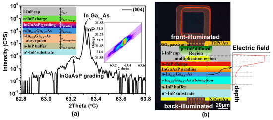
Figure 39.
(a) HR-XRD scan and device layer structure; (b) double side illuminated SAGCM InGaAs/InP APDs with electric field distribution. Reproduced with permission from [93], Elsevier, 2022.
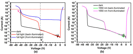
Figure 40.
Electrical properties of the double side illuminated SAGCM InGaAs/InP APDs under (a) a full-spectrum light source and (b) 1550 nm illumination. Reproduced with permission from [93], Elsevier, 2022.
Then, Yiren Chen et al. [94] proposed the selective-area p-type diffusion method to form the back-side illuminated device, which is clearly observed in Figure 41. Single RTD in N2 atmosphere using a Zn3P2/Zn/SiO2 multilayer structure is adopted to realize p-type doping in the InP cap. Extremely high responsivity of 455.5 A/W had been achieved at the reverse voltage of 36.6 V before avalanche breakdown, suggesting that selective-area p-type diffusion is an efficient method to improve the performance of back-illuminated planar InGaAs/InP APD.
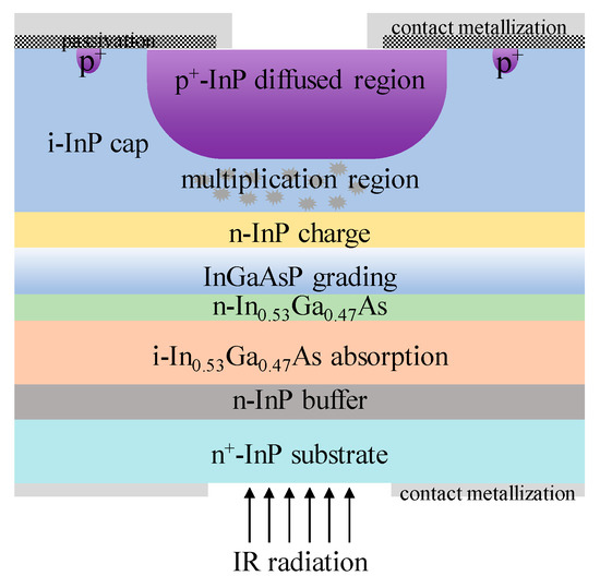
Figure 41.
Schematic diagram and SEM image for the optimized back-illuminated planar InGaAs/InP APD.
Junyang Zhang et al. [95] demonstrated the experimental results for the planar InGaAs/InP-based APDs with different FGR structures. Firstly, the MOCVD system was used to grow the SAGCM InGaAs/InP structure on the 2-inch n+-InP substrate (Figure 42a), which is also passivated by the SiNx and it also has the FGR structure (Figure 42b). After the device is fabricated, the diameter of the FGR region and distance between the diffused p+ region and the FGR region are represented as the L1 and L2, respectively. After careful design, the optimum values for L1 and L2 are 12 μm and 8 μm, respectively (Figure 42c–e). Figure 43a shows the typical I-V characteristics under dark and light illumination for the optimized planar InGaAs/InP-based APDs; both Vpt and Vbr can be extracted. The relationship between the Vbr and L1, L2 is plotted in Figure 43b, and it is clearly observed that the Vbr is less dependent on the values of L1 and L2. The relationship between Vpt and L1 and L2 is also observed in Figure 43b, suggesting that Vpt varies with L1 and L2. To some extent, the variations of L1 and L2 are helpful for edge breakdown suppression. From Figure 43c, dark currents for the device with the L2 of 8–10 μm remain almost the same, which are slightly higher than 1 nA; light currents for the device with various L1 and L2 are shown in Figure 43d, indicating there is a trade-off value for L1 and L2 towards high-performance devices. Responsivity and efficiency were evaluated to be 9.01 A/W and 72% (multiplication gain equals 10), respectively (Figure 43e).
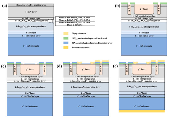
Figure 42.
(a) Cross-sectional diagram, and (b) process flow for the planar geometry SAGCM InGaAs/InP APD with FGR structure, the optimum values for L1 and L2 are 12 μm and 8 μm, respectively(c–e). Reproduced from [95], IEEE, open access, 2022.

Figure 43.
(a) I–V characteristics, (b) punch-through voltage (Vpt) and breakdown voltage (Vbr), (c) dark current curves, (d) light current curves, (e) responsivity/multiplication gain vs. reverse voltage. Reproduced from [95], IEEE, open access, 2022.
F. Signorelli et al. [96] present an InGaAs/InP SAGCM SPAD with high SPDEs and low noise (Figure 44). Improved SPDE is primarily due to the thicker (2 µm) InGaAs absorption region. To avoid the edge breakdown and decrease the charge persistence, a guard ring structure was also introduced. Under the 1550 nm laser illumination, the low temperature (225 K) breakdown voltage and punch through voltage are 68 V and 53 V, respectively. After optimizing the guard ring structure, this device exhibits SPDE up to 53% with a few kpcs DCR at 225 K. The timing jitter is narrow, at 70 ps (FWHM).
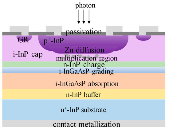
Figure 44.
Schematic diagram of front illuminated InGaAs/InP SAGCM SPADs.
2.3.4. Other Novel InGaAs Avalanche Device Structures
The avalanche phototransistors were used as generators of high-current pulses in the early 1970s. As introduced in Ref. [97], the bias voltages applied to the transistors are set slightly lower than the breakdown voltage at that moment. Then, once a beam of light is illuminated on the device, pairs of electrons and holes are generated and separated by the almost breakdown electric field. Therefore, an avalanche process occurs, and a strong current pulse is obtained. The mechanism of such devices is similar to that of Geiger-mode avalanche photodiodes (GM-APDs). In 1981, on the interdigital electrode architecture, the first base-floating N+-pp-p-N+ avalanche phototransistors (APTs) were proposed by Chen, C. W. on Si platform [98] (Figure 45). The design was accomplished with a symmetric N+-pp-p-N+ structure on a (001) p-type Si substrate. The P- and N-type regions are respectively implanted by boron and arsenic atoms, followed by 1100 °C annealing for 4.5 h.
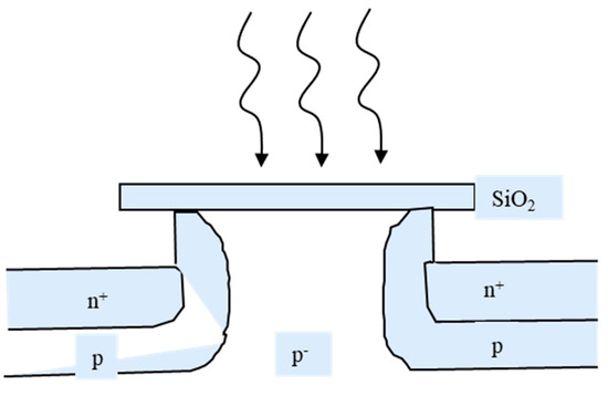
Figure 45.
Schematic device structure of Si N+-pp-p-N+ avalanche phototransistors.
When the device is in operation, the emitter-base junction is forward biased while the opposite p-pn+ junction is reverse biased. To make it work at avalanche mode, the applied voltage should be high enough. When an incident light illuminates the surface of the santireflection layer (SiO2), electron-hole pairs are generated. The generated holes are swept and accumulate in the p region, helping the injection of electrons toward the collector. Then, the electrons are swept into the multiplication layer, and an avalanche occurs. In addition, the p-region on the multiplication side is of course necessary to provide a high-strength field when the forward-bias side prevents the punch-through effect from the avalanche field.
From 1981, after the work of Chen, C. W., Joe C. Compbell moved the APT design toward the InGaAs/InP material system [99,100]. A vertical NPN structure was utilized in those series papers, instead of the interdigital structure. That is, from the bottom, mainly composed by an n-type InP emitter with donor concentration of 2 × 10¹⁷~8 × 1018 cm−3, a thin (~1 μm) p-type In0.53Ga0.47As base with acceptor concentration of 5 × 10¹⁶~5 × 1017 cm−3, and an unintentionally doped (UID) In0.53Ga0.47As collector with donor concentration of 1~5 × 1015 cm−3. Figure 46 demonstrates the device cross-section schematic diagram. In the multiplication layer, the secondary holes are swept back to the base. This motion enhances the accumulation of holes inside the p-type region, increasing the injection of electrons from the emitter. The enhanced injection further improves the primary number of electrons before multiplication, which is positive feedback for the device operation mechanism.
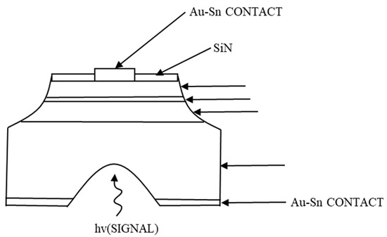
Figure 46.
Cross-section schematic diagram of vertical avalanche heterostructure phototransistors.
The effective current gain G of an APT was also discussed in the article and given by:
where hFE is the common transistor dc current gain and the M represents the avalanche multiplication factor. When the term (M − 1) hFE = 1, the current gain, tending to infinity, leads to device breakdown, and the collector current is only limited by series resistance. The corresponding turn-over voltage is denoted by Vt. When the turn-over voltage excess Vt with (M − 1) hFE >1, the dynamic resistance becomes negative, as shown in Figure 47. Under illumination of P0 (dark environment), 0.5 μW, 0.95 μW, 2 μW, the current increases with larger applied voltages, and the differential conductivity becomes infinity when bias reaches Vt. The minus-resistance portions in Figure 47 are obtained by changing the load line, which hints at the decrease of voltage applied to the transistors with higher Ic.

Figure 47.
I–V characteristic curves of InGaAs/InP APTs under 0.5 μW, 0.95 μW, 2 μW illumination. Reproduced with permission from [100], IEEE, 2014.
Shi, JW improved the structure of III–V APTs by adding In0.52Al0.48As avalanche p-i-n junction beneath the collector. By this design, they moved the separated-absorption-charge-multiplication (SACM) structure in conventional APDs to the APTs [101]. The schematic cross-section picture and corresponding profiles in each layer are demonstrated in Figure 48a. Upper to the In0.52Al0.48As avalanche junction, an UID 50-nm graded InAlGaAs layer is inserted to smooth the energy band offset between the In0.53Ga0.47As collector and the lower In0.52Al0.48As multiplication layers. The p-type In0.52Al0.48As charger does not only provide a strong field, but it also prevents the punch-through effect on the intrinsic In0.53Ga0.47As collector. Figure 48b shows the operation bandwidth as a function of device current gain, concluding that at bias = 6 V, the highest gain-bandwidth couple can be achieved at ~90 THz. A very short response time of about ~160 ps can be obtained with a light pulse of 0.08 pJ/pulse.

Figure 48.
(a) The cross-section schematic diagram of APTs and structure profiles, (b) bandwidth and response time curves as a function of gain.
In conclusion, for APTs, the gain changes with various incident powers, even at the same bias. This feature is due to the enhanced hole accumulation in the base under illumination, resulting in a higher transistor current gain hFE and a lower sufficient multiplication factor M, e.g., a lower VCE. It means that if APTs are utilized in some applications with uncertain incident power, the applied bias is hard to choose, which would limit the range of applications. In energy-band design, a wider energy-gap material is always utilized as the emitter. Such materials increase the energy barrier between the emitter and base, helping the accumulation of carriers inside the base. In addition, because the avalanche region is induced, the multiplication layer designs of APDs can be taken into consideration, such as the SACM structure, low-k, and wide energy-band materials.
3. SWIR APDs Focal Plane Arrays (FPAs)
For sensitivity in the SWIR wavelength range, InGaAs/InP pixel array chips were generally accepted owing to their excellent absorption properties in this range. However, they are not able to be integrated into CMOS. Ge/Si APDs are cheaper to produce and compatible with the traditional CMOS technology, but there are some problems with sensitivity and noise levels in this range. For high-performance Ge/Si APDs, a 4% lattice mismatch between Si and Ge makes the implementation of low-cost pixel arrays more challenging.
3.1. Ge/Si APDs FPAs
In 2016, Amir Sammak et al. [102] demonstrated the CMOS-compatible Ge/Si APD pixel arrays. To achieve high-quality Ge/Si APD, the pure gallium and pure boron (PureGaB) Ge/Si process was introduced. This way, the defect level for the Si/Ge interface maintains a very low level after the PureGaB deposition. Arrays of 300 × 1 pixels were integrated on the n-type Si (100) substrate. Figure 49 shows the basic process flow for PureGaB Ge/Si APDs, which is as follows: (I) grow 30 nm thermal SiO2 on a Si substrate; (II) deposit 1 μm SiO2 on thermal SiO2/Si via low pressure CVD; (III) pattern the SiO2 layer; (IV) etch on the Si surface and define the APD areas. For the accuracy of the characterization results, it is essential that all the Ge/Si APD pixel arrays were uniformly exposed to the incident light.
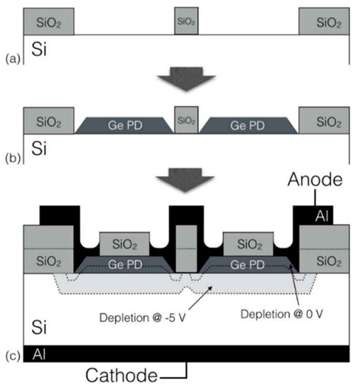
Figure 49.
Process flow for PureGaB Ge/Si APDs, (a) open the window through SiO2 to Si, (b) deposit the Ge/Si PDs in the windows, (c) form the Al contact. Reproduced from [102], IEEE, open access, 2015.
Based on the above-mentioned planar Ge/Si SPAD structure, detector arrays can be fully processed by Si CMOS technology. In 2020, KATERYNA et al. [103] reported the demonstration of LIDAR 3D imaging using planar geometry Ge/Si SPAD at a wavelength of 1450 nm (“eye-safe” consideration). Figure 50 shows the depth and intensity profile measurements reconstructed using the pixel-wise cross-correlation approach by altering the per-pixel acquisition time. For a pixel acquisition time of 0.5 ms, the average number of photons per pixel over the entire scene was 1.4 photons per pixel. As expected, the quality of image reconstruction degrades as the acquisition time is reduced, becoming difficult to discern in isolation at the 0.5 ms acquisition time per pixel. Several algorithms have been developed to restore depth and intensity images in extreme cases, such as photon-starved regimes, including RDI-TV, ManiPoP, UA, and NR3D. In this paper, we highlight the benefit that both the RDI-TV algorithm and the ManiPoP algorithm provide in reducing the acquisition time.

Figure 50.
Depth and intensity profile measurements were reconstructed using the pixel-wise cross-correlation approach with the per-pixel acquisition times. Reproduced from [103], Optica Publishing, open access, 2020.
3.2. InGaAs APDs FPAs
Since InGaAs/InP and InGaAs/InAlAs SAGCM APDs have been studied for several decades, which means there are already mature products on the market [104,105,106]. Herein, typical InGaAs APD FPAs were selected to review its current progress.
Mark A. Itzler et al. [107] demonstrated the planar-geometry InGaAs/InP APDs with 32 × 32 FPAs, which are also hybridized to the CMOS ROICs in order to enable the ToF measurement for each pixel (Figure 51). To check the performance, both SPDE measurements and DCR measurements were carried out. Both full FPA maps operating at 1.06 µm and 1.55 µm were demonstrated. For the 1.06 µm FPAs, SPDE is higher than 40% with DCRs of 20 kHz at 250 K (Figure 52a). In the whole FPAs, average DCRs were evaluated to be 13.6 kHz, and a standard deviation of 4.2 kHz also existed (Figure 52b). As for the SPDEs distribution, the average SPDE is around 39%, which has a 6.3 % deviation. Both the deviations of the DCRs and SPDEs were mainly attributed to the variation of the APD breakdown voltage (Vb), which can be corrected by using non-uniformity correction factors.
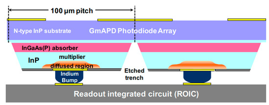
Figure 51.
Schematic diagram of planar-geometry InGaAs/InP APD FPAs contacted to CMOS readout ICs via in-bump flip-chip bonding. Reproduced with permission from [107], IEEE, 2010.
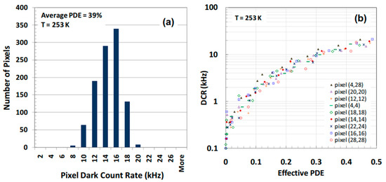
Figure 52.
(a) Pixel DCRs distribution for the InGaAs/InP FPAs at 1.06 µm; (b) SPDE-dependent DCRs. Reproduced with permission from [107], IEEE, 2010.
To meet the eye-safety requirement, 1.55 µm FPAs had also been checked at 250 K. In the whole FPAs, average DCRs were evaluated to be 28 kHz and standard deviation as about 6.5 kHz (Figure 53a). As for the SPDE distribution, the mean SPDE is around 22.2%, which has a 4.6% deviation (Figure 53b). Both the deviations of the DCRs and SPDEs were mainly attributed to the variation of the APD breakdown voltage (Vb).
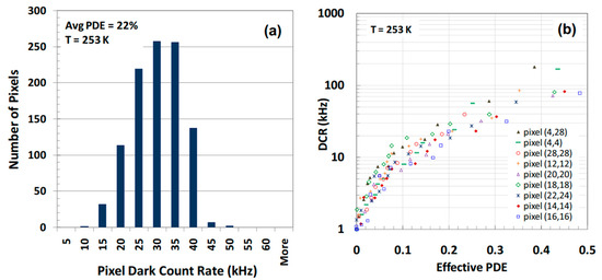
Figure 53.
(a) Pixel DCRs distribution for the InGaAs/InP FPAs at 1.55 µm; (b) SPDE-dependent DCRs. Reproduced with permission from [107], IEEE, 2010.
3.3. Challenges
3.3.1. Challenges for Ge(GeSn)/Si APDs
From all the above-mentioned reported results, Ge/Si APDs are all directly sitting on the Si platform. However, device performance is not available for large-scale commercialization. There are several challenges that need to be overcome.
Firstly, TDDs in the Ge absorption layer are still high. To eliminate the TDDs, numerous strategies were proposed in recent decades, including doped Ge buffer layers [108,109,110], compositionally graded SiGe buffer layers [111,112,113], ultra-thin Si/SiGe superlattice buffer layers [114,115], high temperature annealing [116,117,118], three-step growth [119,120], the selective epitaxial growth (SEG) method [121,122,123], etc. With the continuous effort focused on decreasing the TDDs in the Ge layer, the TDDs for the top Ge layer were evaluated to be in the orders of 106–107 cm−2. However, the defective level between the Si substrate and Ge layer is extremely high (usually 109–1010 cm−2), which hinders the low dark current and low DCR Ge/Si APDs. Therefore, suppression of the dark current density is the main topic for high-performance Ge/Si APDs. To solve this problem, researchers proposed the wafer-bonding technique to achieve the low TDDs of the Ge layer on the insulator, which is expected to decrease the dark current as much as possible. Based on the wafer-bonding technique, Shaoying Ke et al. [124] theoretically investigated the wafer-bonded Ge/Si APDs in terms of tunneling effect and interface state (Figure 54). A thin GeO2 insulator layer is inserted between the Ge absorption layer and the Si charge layer. With the increasing GeO2 thickness, photocurrent is greatly decreasing due to the reduction of tunneling possibilities and carrier accumulation in the Ge absorption layer. Furthermore, interface state densities (ISDs) play a vital role in improving the APD gain and 3dB-BW (bandwidth) at lower bias. There is also a novel APD structure proposed on the germanium on insulator (GOI) platform [125], which was shown in Figure 55. However, this structure has not been experimentally achieved yet. More efforts should be made to process the wafer-bonding Ge/Si APDs, which are very important for the commercial application.

Figure 54.
Schematic of wafer-bonded Ge/Si APDs with Ge/GeO2 interface state and GeO2/Si interface state.
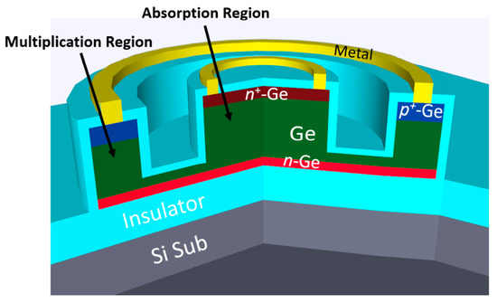
Figure 55.
3D Schematic of wafer-bonded Ge APDs on the GOI platform. Reproduced from [125], open access by NTU Library, 2021.
Another strategy for optimizing the device performance is the introduction of Ge/graded-SiGe heterostructures in the multiplication layer, which is helpful for controlling the impact ionization. It should be noted that Si is one of the best materials for the multiplication layer in terms of low-noise operation due to its ratio of electron and hole ionization coefficients being far from unity (~0.01). However, smaller ionization coefficients lead to high operation voltages, which are 2~3 times higher than those for Ge/Si APDs. In Ge, the ionization coefficient for holes is slightly higher than that for electrons. Thus, excess noises were reduced by enhancing the ionization coefficient for holes. Using the Ge/graded-SiGe heterostructure in multiplication is one option to suppress the excess noise. Figure 56 shows the typical I–V curves and responsivity spectra biased at 3 V, it can be clearly observed that the performance of each device is comparable, suggesting this strategy is promising for low-noise and low-voltage APD applications [126].
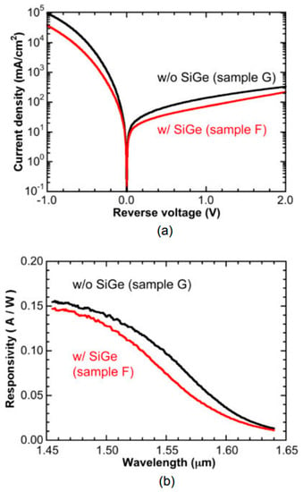
Figure 56.
(a) Typical I-V characteristics without illumination; (b) responsivity spectra biased at 3 V (w/o SiGe and w/SiGe indicate without SiGe and with SiGe, respectively). Reproduced with permission from [126], IOP Publishing, 2016.
Bandgap properties for GeSn material can be tuned by changing the incorporation of Sn into Ge, which makes it suitable as the absorption layer for the Si-based low-cost SWIR APDs, especially for the eye-safe 1550 nm light detection. To grow the high-quality GeSn materials, several growth methods were explored, including MBE, PVD, and CVD. Up until now, great breakthroughs had been made for high-Sn-composition material growth. Especially for CVD growth, this is the most promising method to grow high-quality materials with high Sn composition [127,128,129,130,131,132,133,134]. From the device perspective, although linear mode GeSn APDs have been demonstrated experimentally, GeSn growth techniques are facing several bottlenecks, such as Sn segregation during growth and after annealing, which leads to severe surface roughness and affects the material properties [135,136,137,138,139,140,141]. Other issues include uniformity in the GeSn absorption layer, Si/Ge interface and Ge/GeSn interface quality, the existence of point defects in direct bandgap GeSn, etc. Similar to the Ge defect reduction strategies, such as doped buffer layers, compositionally graded buffer layers, ultra-thin superlattice buffer layers, high temperature H2 annealing, cyclic thermal annealing, and the selective epitaxial growth (SEG) method, were also needed to investigate the defect suppression mechanism for GeSn materials [142]. Apart from the GeSn growth difficulties, there is little theoretical modeling research on the GeSn APDs, which hinders device design and performance prediction. Due to the missing parameter for GeSn, the majority of simulation results are not described accurately [143,144,145,146,147,148]. Therefore, in-depth and accurate GeSn material parameters studies are required, whether experimentally or theoretically.
From the device structure perspective, a large amount of Ge(GeSn) APDs were SACM structures. In this structure, Si was always adopted as the multiplication layer owing to its ionization rate ratio, which varies considerably with electric field. However, the lattice parameter mismatch between Si and Ge(GeSn) is also large. To achieve high performance Ge(GeSn) APDs, it usually needs to weigh the advantages and disadvantages of the Si multiplication layer and defect level among the total device structure (Si/Ge interface and Ge absorption). To give attention to these two factors, more innovative devices are required to be proposed. Moreover, only a few groups are working on the planar-geometry Ge(GeSn) APDs, but more efforts should be devoted due to its excellent SPDE.
Emerging group IV material systems, such as GeSnSi alloys [149], GeSnSiC alloys [150,151], GePb alloys [152,153,154], and GeSnPb alloys [155], are also promising SWIR absorbers towards high-performance APDs. Especially for the GeSnSiC alloys, Ge1−x−y−zSnxSiyCz films (0.01 ≤ x ≤ 0.06, 0 ≤ y ≤ 0.02 and 0 ≤ z ≤ 0.01) had been successfully grown at 280–330 °C on Ge and Si using commercial RPCVD technique, indicating it has the great potential to be commercialized. Moreover, GeSnSiC alloys are also important for future Si-based monolithic integration [156]. To further improve the device performance, quantum well structures [157,158] and quantum dots multilayer structures [159] are also feasible for the enhancement of SWIR detection. For the APD devices, the multiplication effect also plays a vital role in the device’s performance. However, the large lattice mismatch between Si and Ge(GeSn) is the main hurdle for the high-performance Ge(GeSn) APDs. To balance the multiplication effect and lattice mismatch problem, the SiGe layer is also an important candidate for the multiplication region due to its CMOS process compatibility, relatively strong avalanche effect, and smaller lattice mismatch with Ge and GeSn [160,161,162,163]. Moreover, SiGeC is a conspicuous choice for the multiplication region, which is helpful for the temperature coefficient of resistance and low noise level [164,165]. To lower the contact resistance, the nickel strategy is widely used at low temperatures (compared to Co) for forming the Ni-Si, Ni-SiGe, Ni-Ge, and Ni-GeSn ohmic contacts [166,167,168,169,170,171].
3.3.2. Challenges for InGaAs/InP APDs and InGaAs/InAlAs APDs
From the reviewed articles above, it was clear that the majority of the InGaAs APDs were grown on the InP substrate by the MBE and MOCVD tools. As is known to all, InP substrates are smaller and extremely expensive, which makes their commercial cost very expensive. To push the InGaAs APDs towards cost-effective LiDAR applications, several problems need to be solved.
Firstly, low-cost and large size wafer should be developed, such as, GaAs and Si. For the GaAs case, wafer size can reach up to 6 or 8 inches now, but there is lattice mismatch and thermal mismatch between the GaAs substrate and InP layers; for the Si case, there are always 8 inch, 12 inch, or even 18 inch wafers, which also have the problems of thermal mismatch, lattice mismatch, and polarity contrast between the Si substrate and InP layers. Compared to the GaAs substrate, there are more problems that need to be dealt with for the Si substrate. More explorative investigations should be conducted to overcome the growth obstacles. Thus, cost-effective InGaAs APDs will be achievable, and the LiDAR price will also be lower [172,173,174,175,176,177,178,179].
Secondly, InGaAs/InAlAs APDs have the great potential to substitute the InGaAs/InP APDs, which makes it very important to grow the high-quality InAlAs multiplication layers. Although InGaAs/InP APDs have been commercialized for a long time, there is still room to improve the device’s performance. Especially from the defect reduction and multiplication gain enhancement perspectives, which will greatly improve the device performance. Until now, InP and InAlAs layers were employed as the multiplication region; Si is also a promising candidate for the multiplication region [180,181,182,183,184,185]. Wafer-bonded InGaAs/Si APDs were proposed to greatly improve the device performance (Figure 57), which gives researchers a novel technical route to optimize the device architecture [186].
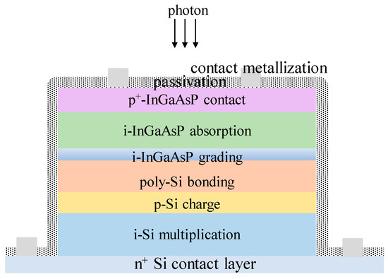
Figure 57.
Wafer-bonded InGaAs/Si SAGCM APDs.
Despite the growth and device structure issues, effective passivation technology is of great significance to improving the performance and stability of the device. The properties of many semiconductor devices are closely related to the surface properties of semiconductors. In some cases, it is often not the in vivo effect of semiconductors but the surface effects that govern the characteristics of semiconductor devices [187]. For mesa-type infrared detectors, surface properties are often the key factor affecting the final performance of the device. The quality of the surface condition is an important source of device noise, and it is an important factor causing the crosstalk of multiple components. Large-scale FPA detectors with smaller spacing can now be created, thereby improving the resolution of the image. However, as the spacing of the mesa detector arrays decreases, the signal-to-noise ratio also decreases [188]. The mesa detector etching process resulted in the appearance of dangling bonds on the side walls, which causes a high surface leakage current [189]. These bonds hanging from the surface of the InGaAs region of the InGaAs/InP photodetector significantly affect the stability of the dark current [190]. Surface leakage has a great impact on the performance of photovoltaic devices. At the same time, the size of the surface composite speed determines the performance of the optical conductivity device. The high surface density of states and the surface composite rate have been restricted to the development of III–V family semiconductor devices, and they need to be solved by surface passivation. The purpose of passivation is to protect the surface from external pollution and damage and reduce the surface density of states, surface recombination rate, and side leakage current, so as to reduce the dark current of the detector [191], improve the detection rate, and ensure the long-term stability of the device. In order to obtain excellent semiconductor surface interface properties, on the one hand, it is necessary to effectively remove the semiconductor surface pollutants to achieve a pure surface and effectively prevent a pure semiconductor surface from being exposed to air or insulation layer interface pollution or oxidation, namely chemical passivation; on the other hand, it is necessary to effectively reduce the interface state density between the insulating layer and the semiconductor material, namely electrical passivation. The passivation process is an essential and very critical process for semiconductor device preparation, and tremendous studies have been conducted and many effective methods have been summarized.
Before growing passivation films using techniques such as chemical vapor deposition, atomic layer deposition, or organic passivation and surface thiolation, it is often necessary to perform some auxiliary treatment on the semiconductor surface first to remove surface pollutants, impurity ions, and the air oxide layer. The common methods mainly include chemical solvent treatment, plasma cleaning, special gas treatment, and light treatment [192,193,194,195,196,197,198]. (a) Chemical solvent treatment, chemical solvents treatment commonly used organic solvents are: alcohol, acetone, methanol, trichloroethylene, etc.; inorganic solvents include dilute hydrochloric acid, sodium hydroxide/potassium, hydrofluoric acid, and other solutions. These solvents can effectively remove the vast majority of organic matter, oxides, and impurities on the semiconductor surface. (b) Plasma cleaning, of the adhesion force of the passivation layer film to the semiconductor surface, is not only dependent on the type of substrate material but is also affected by the surface residues. Before depositing the passivation film, the plasma precleaning of the material surface can effectively improve the adhesion force between the film and the substrate material. Studies have shown that hydrogen plasma can effectively remove inorganic residues, and oxygen plasma can effectively remove organic residues. The hydrogen plasma pre-cleaning process before the film deposition can effectively improve the quality of the deposited film and its adhesion to the substrate material. For example, the NH3 plasma pre-cleaning process can decompose NH3 into N and H atoms. H atoms acting on the surface can form a hydrogenated surface layer, forming a beneficial interlayer between the film and the substrate. Jianqiang Lin et al. studied PH3 plasma passivation on the InGaAs surface of the MOS device. (c) Special gas treatment is similar to plasma cleaning, before depositing the film, the semiconductor surface through H2; trimethyl aluminium (TMA) can also play a certain role in removing oxides, impurities, and dangling bonds. Wipakom Jevasuwan et al. studied the TMA passivation process and interface formation process of an InGaAs MISFET device. (d) Light treatment: R.Driad et al. studied the passivation process of the material surface of InGaAs in the InGaAs/InP structure HBT device and used ultraviolet radiation (UV) and ozone (O3) treatment to effectively remove the organic and inorganic materials on the semiconductor surface. Through XPS analysis, it was found that the UV-O3 treatment removed the surface defect layer, forming oxides such as As2O3, As2O5, In2O3, and Ga2O3. The semiconductor surface material components basically showed the stoichiometric ratio, and the device performance was also significantly improved. For III–V compound semiconductor devices, the commonly used medium passivation film mainly includes SiNx, SiO2, A12O3, BCB, Polyimide (PI), and other organic passivation films, sometimes using SiO2-SiNx or SiO2-PI multilayer passivation film structures. The combined use of two passivation films can effectively achieve the advantages of two films while also achieving stress compensation.
Ohmic contact is one of the most important processes in the preparation of semiconductor devices, which has an important influence on the performance, reliability, and stability of the devices. Good metal-semiconductor ohmic contacts can be obtained in the following ways: (a) Low-barrier connection. If the barrier formed by the formation between the metal and semiconductor contact is low, there are enough carriers at room temperature to enter the metal from the semiconductor or from the metal into the semiconductor; such contacts have minimal rectification effect. (b) High composite contact. The introduction of many strong composite centers in the vicinity of the metal-semiconductor contact surface constitutes a high composite contact. The high composite contacts do not inject the nonequilibrium carriers into the semiconductor, because the original nonequilibrium minority carriers that may have been injected into the body are lost when they pass through the high composite contact zone. The high composite contacts will also not have a rectification effect because, in the reverse, the high composite center will become the high generation center, making the reverse current change very large, and the reverse high resistance state will not exist. If the semiconductor surface is damaged, crystal defects may form near the surface, and their role is similar to that of the compound center. If the composite center density is high enough, the recombination in the depletion zone will become the main conductive mechanism, so that the contact resistance decreases significantly. (c) High doping contact. At the metal contact position of the semiconductor surface and the metal, if a high concentration of donor or acceptor impurities is added first, the high doping contact is formed. On the one hand, the highly doped n+ or p+ layer can effectively reduce the injection of nonequilibrium carriers, while the depletion layer region is very thin and easy to produce field emission, so the contact has a very low resistance at zero bias.
The characterization of metal-to-semiconductor contact characteristics is the specific contact resistance per unit area metal-to-semiconductor contact differential resistance. Specific contact resistance, or the interface resistance of ohmic contact, cannot be directly measured. The contact zone generally includes a metal layer, a metal-semiconductor interface, and a semiconductor junction. In addition, various parasitic resistances have been introduced. Currently, many testing methods based on different models are already available. However, no matter what the method, under a certain constant current, measure the voltage between some contact points, find the respective resistance, and then according to different physical models, from the total resistance deduct various parasitic resistances, and finally achieve the specific contact resistance. For family InP compound semiconductors, P-type ohmic contact is generally much more difficult to make than n-type, firstly because the effective mass of the hole is larger than the electron, and secondly because it is determined by the device processing process itself [199,200,201]. We also summarize the evidence and the pros and cons for Ge (GeSn) and InGaAs APDs in Table 3.
Table 3.
Summarized evidence of the pros and cons for Ge (GeSn) and InGaAs APDs.
4. Conclusions and Perspectives
In this article, we review the recent research progress for the mesa- and planar-geometry InGaAs APDs, which are commonly grown by the MBE or MOCVD technique on the InP substrate. Due to the lattice match between InGaAs and InP or InAlAs, both InP or InAlAs and InGaAs were employed as the multiplication region and absorption region, respectively. To improve the device performance, SAGCM structure InGaAs/InP APDs were generally acknowledged. For the InGaAs APDs with the InAlAs multiplication layer, a higher gain at a low dark current level is obtained. Therefore, InP is gradually replaced by the InAlAs multiplication region owing to its superior ionization coefficients, which reduce the excess noise. At the same time, InAlAs offers a wider bandgap, which is also helpful for reducing the tunneling current. InGaAs APDs with both mesa- and planar-geometry were surveyed, including front-side illumination, multi-mesas, MIM optical microcavities, backside illumination, double-side illumination, FGR structure, and APTs. Although InGaAs APDs have been commercialized for a long time, more explorative investigations should be conducted to overcome the growth obstacles, which will greatly knock down the price of InGaAs APDs.
The Ge (GeSn) material for the APD application has also been reviewed. To improve the device performance, several strategies are proposed, including planar-geometry, an enhanced multiplication layer, photo-trapping microstructure, SEG growth, a multi-mesa structure, photonic crystal enhancement, etc. Among all these strategies, planar geometry features the best performance in terms of SPDE, DCRs, NEP, jitter, and 3D imaging quality. However, the main obstacle to the commercialization of Ge(GeSn)/Si APDs is the high TDD in the whole Ge(GeSn) structure, which leads to high DCRs. Until now, the majority of Ge(GeSn)/Si APDs used Si as the multiplication region. Therefore, there is an urgent need to design and develop more innovative GeSn(Sn) APD structures, which would further pave the way for the huge advancement of the next generation of high-sensitivity SWIR detection systems.
Author Contributions
Conceptualization, Y.M. and H.H.R.; literature survey, Y.M., X.Z., H.L., Y.D., B.L. (Ben Li), C.H., T.D., J.D., Z.Z., J.S., H.W., B.L. (Bin Lu) and L.D.; formal analysis, Y.M., H.H.R., L.D.; project administration, H.H.R.; supervision, H.H.R.; writing—original draft preparation, Y.M.; writing—review and editing, Y.M. and H.H.R. All authors have read and agreed to the published version of the manuscript.
Funding
This work was supported by Guangdong Province Research and Development Program in Key Fields (Grant No. 2021B0101280002), Guangzhou City Research and Development Program in Key Fields (Grant No. 202103020001) and the National Natural Science Foundation of China (Grant No. 92064002).
Data Availability Statement
The data presented in this study are available on request from the corresponding authors.
Conflicts of Interest
Authors declare no conflict of interest.
References
- Moeen, M.; Kolahdouz, M.; Salemi, A.; Abedin, A.; Östling, M.; Radamson, H.H. Improved designs of Si-based quantum wells and Schottky diodes for IR detection. Thin Solid Films 2016, 613, 19–23. [Google Scholar] [CrossRef]
- Conley, B.R.; Margetis, J.; Du, W.; Tran, H.; Mosleh, A.; Ghetmiri, S.A.; Tolle, J.; Soref, R.; Li, B.; Naseem, H.; et al. Si based GeSn photoconductors with a 1.63 A/W peak responsivity and a 2.4 μm long-wavelength cutoff. Appl. Phys. Lett. 2014, 105, 221117. [Google Scholar] [CrossRef]
- Zhao, X.; Moeen, M.; Toprak, M.S.; Wang, G.; Luo, J.; Ke, X.; Li, Z.; Liu, D.; Wang, W.; Zhao, C.; et al. Design impact on the performance of Ge PIN photodetectors. J. Mater. Sci. Mat. Electron. 2020, 31, 18–25. [Google Scholar] [CrossRef]
- Dong, L.; Yu, J.; Jia, R.; Hu, J.; Zhang, Y.; Sun, J. Self-powered MSM deep-ultraviolet β-Ga2O3 photodetector realized by an asymmetrical pair of Schottky contacts. Opt. Mater. Exp. 2019, 9, 1191–1199. [Google Scholar] [CrossRef]
- Kumar, H.; Basu, R. Effect of defects on the performance of Si-based GeSn/Ge mid-infrared phototransistors. IEEE Sens. J. 2020, 21, 5975–5982. [Google Scholar] [CrossRef]
- Chen, B.; Wan, Y.; Xie, Z.; Huang, J.; Zhang, N.; Shang, C.; Norman, J.; Li, Q.; Tong, Y.; Lau, K.; et al. Low dark current high gain InAs quantum dot avalanche photodiodes monolithically grown on Si. ACS Photonics 2020, 7, 528–533. [Google Scholar] [CrossRef]
- Craig, A.P.; Jain, M.; Meriggi, L.; Cann, T.; Niblett, A.; Collins, X.; Marshall, A.R.J. Extended short-wave infrared linear and Geiger mode avalanche photodiodes, based on 6.1 Å materials. Appl. Phys. Lett. 2019, 114, 053501. [Google Scholar] [CrossRef]
- Chapman, D.C.; Vineis, C.J.; Oakley, D.C.; Napoleone, A.; Smith, G.M.; Duerr, E.K.; Jensen, K.E.; Donnelly, J.P.; McIntosh, K.A.; Verghese, S. Growth and characterization of GaInAsP/InP-based Geiger-mode avalanche photodiodes. J. Cryst. Growth 2008, 310, 2365–2369. [Google Scholar] [CrossRef]
- Marshall, A.R. The InAs Electron Avalanche Photodiode. In Advances in Photodiodes; IntechOpen: London, UK, 2011. [Google Scholar]
- Manis-Levy, H.; Shikler, R.; Golan, Y.; Sarusi, G. High photoconductive gain in a GaAs/PbS heterojunction based SWIR detector. Appl. Phys. Lett. 2020, 117, 081107. [Google Scholar] [CrossRef]
- Pandey, A.K.; Basu, R.; Chang, G.E. Optimized Ge1−xSnx/Ge Multiple-Quantum-Well Heterojunction Phototransistors for High-Performance SWIR Photodetection. IEEE Sens. J. 2018, 18, 5842–5852. [Google Scholar] [CrossRef]
- Chen, B.; Jiang, W.; Yuan, J.; Holmes, A.L.; Onat, B.M. SWIR/MWIR InP-based pin photodiodes with InGaAs/GaAsSb type-II quantum wells. IEEE J. Sel. Top. Quantum Electron. 2011, 47, 1244–1250. [Google Scholar] [CrossRef]
- Iiyama, K.; Takamatsu, H.; Maruyama, T. Hole-Injection-Type and Electron-Injection-Type Silicon Avalanche Photodiodes Fabricated by Standard 0.18-μm CMOS Process. IEEE Photonics Technol. Lett. 2010, 22, 932–934. [Google Scholar] [CrossRef]
- Baron, A.Q.; Kishimoto, S.; Morse, J.; Rigal, J.M. Silicon avalanche photodiodes for direct detection of X-rays. J. Synch. Radiat. 2006, 13, 131–142. [Google Scholar] [CrossRef]
- Menkara, H.M.; Wagner, B.K.; Summers, C.J. Gain properties of doped GaAs/AlGaAs multiple quantum well avalanche photodiode structures. Appl. Phys. Lett. 1995, 66, 1764–1766. [Google Scholar] [CrossRef]
- Saleh, M.A.; Hayat, M.M.; Saleh, B.E.; Teich, M.C. Dead-space-based theory correctly predicts excess noise factor for thin GaAs and AlGaAs avalanche photodiodes. IEEE Trans. Electron. Devices 2000, 47, 625–633. [Google Scholar] [CrossRef]
- Ribordy, G.; Gisin, N.; Guinnard, O.; Stuck, D.; Wegmuller, M.; Zbinden, H. Photon counting at telecom wavelengths with commercial InGaAs/InP avalanche photodiodes: Current performance. J. Modern Opt. 2004, 51, 1381–1398. [Google Scholar]
- Jung, J.; Kwon, Y.H.; Hyun, K.S.; Yun, I. Reliability of planar InP-InGaAs avalanche photodiodes with recess etching. IEEE Photonics Technol. Lett. 2002, 14, 1160–1162. [Google Scholar] [CrossRef]
- Sandall, I.C.; Zhang, S.; Tan, C.H. Linear array of InAs APDs operating at 2 µm. Opt. Express 2013, 21, 25780–25787. [Google Scholar] [CrossRef]
- Alimi, Y.; Pusino, V.; Steer, M.J.; Cumming, D.R.S. InSb avalanche photodiodes on GaAs substrates for mid-infrared detection. IEEE Trans. Electron. Devices 2019, 67, 179–184. [Google Scholar] [CrossRef]
- Shen, C.; Yang, L.; Guo, H.-J.; Yang, D.; Chen, L.; He, L. Numerical simulation of high-operating-temperature MWIR HgCdTe APD detectors. J. Infrared. Millimeter. Waves. 2021, 40, 576. [Google Scholar]
- Tsybrii, Z.; Bezsmolnyy, Y.; Svezhentsova, K.; Vuichyk, M.; Lysiuk, I.; Apatska, M.; Smolii, M.; Dmytruk, N.; Bunchuk, S.; Andreeva, K.; et al. HgCdTe/CdZnTe LPE epitaxial layers: From material growth to applications in devices. J. Crys. Growth 2020, 529, 125295. [Google Scholar] [CrossRef]
- Shen, G.; Zheng, T.; Li, Z.; Wu, E.; Yang, L.; Tao, Y.; Wang, C.; Wu, G. High-speed airborne single-photon LiDAR with GHz-gated single-photon detector at 1550 nm. Opt. Laser. Technol. 2021, 141, 107109. [Google Scholar] [CrossRef]
- Spuler, S.M.; Mayor, S.D. Scanning eye-safe elastic backscatter lidar at 1.54 μ m. J. Atmospheric. Oceanic. Tech. 2005, 22, 696–703. [Google Scholar] [CrossRef]
- Zhao, X.; Wang, G.; Lin, H.; Du, Y.; Luo, X.; Kong, Z.; Su, J.; Li, J.; Xiong, W.; Miao, Y.; et al. High performance pin photodetectors on Ge-on-insulator platform. Nanomaterials 2021, 11, 1125. [Google Scholar] [CrossRef]
- Miao, Y.; Wang, G.; Kong, Z.; Xu, B.; Zhao, X.; Luo, X.; Lin, H.; Dong, Y.; Lu, B.; Dong, L.; et al. Review of Si-Based GeSn CVD Growth and Optoelectronic Applications. Nanomaterials 2021, 11, 2556. [Google Scholar] [CrossRef]
- Mathews, J.; Roucka, R.; Xie, J.; Yu, S.Q.; Menéndez, J.; Kouvetakis, J. Extended performance GeSn/Si (100) p-i-n photodetectors for full spectral range telecommunication applications. Appl. Phys. Lett. 2009, 95, 133506. [Google Scholar] [CrossRef]
- Tran, H.; Pham, T.; Du, W.; Zhang, Y.; Grant, P.C.; Grant, J.M.; Sun, G.; Soref, R.; Margetis, J.; Yu, S.Q.; et al. High performance Ge0. 89Sn0. 11 photodiodes for low-cost shortwave infrared imaging. J. Appl. Phys. 2018, 124, 013101. [Google Scholar] [CrossRef]
- Tran, H.; Pham, T.; Margetis, J.; Zhou, Y.; Dou, W.; Grant, P.C.; Grant, J.M.; Al-Kabi, S.; Sun, G.; Soref, R.A.; et al. Si-based GeSn photodetectors toward mid-infrared imaging applications. ACS Photonics 2019, 6, 2807–2815. [Google Scholar] [CrossRef]
- Zhou, H.; Xu, S.; Wu, S.; Huang, Y.C.; Zhao, P.; Tong, J.; Son, B.; Guo, X.; Zhang, D.; Gong, X.; et al. Photo detection and modulation from 1,550 to 2,000 nm realized by a GeSn/Ge multiple-quantum-well photodiode on a 300-mm Si substrate. Opt. Express 2020, 28, 34772–34786. [Google Scholar] [CrossRef]
- Bowers, J.E.; Ramaswamy, A.; Dai, D.; Zaoui, W.S.; Kang, Y.; Yin, T.; Morse, M. Recent advances in Ge/Si PIN and APD photodetectors. Phys. Status Solidi C 2010, 7, 2526–2531. [Google Scholar] [CrossRef]
- Stokoe, J.C.D.; Putland, P.A.; Sutherland, R.R. A review of reliability evaluation techniques applied to InGaAs PIN photodiodes, Germanium APDs and InGaAs APDs. Qual. Reliab. Eng. Int. 1989, 5, 319–329. [Google Scholar] [CrossRef]
- Liang, Y.; Lin, G.; Su, X.; Zhang, X.; Feng, S.; Xu, Y.; Li, C. A review on III-V compound semiconductor short wave infrared avalanche photodiodes. Nanotechnology 2022, 33, 222003. [Google Scholar] [CrossRef]
- Izhnin, I.I.; Lozovoy, K.A.; Kokhanenko, A.P.; Khomyakova, K.I.; Douhan, R.M.; Dirko, V.V.; Akimenko, N.Y. Single-photon avalanche diode detectors based on group IV materials. Appl. Nano 2022, 12, 253–263. [Google Scholar] [CrossRef]
- Xie, S. Design and Characterisation of InGaAs High Speed Photodiodes, InGaAs/InAlAs Avalanche Photodiodes and Novel AlAsSb Based Avalanche Photodiodes. Ph.D. Thesis, University of Sheffield, Sheffield, UK, 2012. [Google Scholar]
- Huang, M.; Li, S.; Cai, P.; Hou, G.; Su, T.I.; Chen, W.; Pan, D. Germanium on silicon avalanche photodiode. IEEE J. Sel. Top. Quantum Electron. 2017, 24, 1–11. [Google Scholar] [CrossRef]
- Xiang, J.; Zhao, Y. Comparison of waveguide avalanche photodiodes with InP and InAlAs multiplication layer for 25 Gb/s operation. Opt. Eng. 2014, 53, 046106. [Google Scholar] [CrossRef]
- Cai, H.; Qian, K.; An, Y.; Lin, G.; Wu, S.; Ding, H.; Huang, W.; Chen, Y.; Wang, Y.; Li, C. Thickness-dependent behavior of strain relaxation and Sn segregation of GeSn epilayer during rapid thermal annealing. J. Alloys Compd. 2022, 904, 164068. [Google Scholar] [CrossRef]
- Ni, W.X.; Ekberg, J.O.; Joelsson, K.B.; Radamson, H.H.; Henry, A.; Shen, G.D.; Hansson, G.V. A silicon molecular beam epitaxy system dedicated to device-oriented material research. J. Crys. Growth 1995, 157, 285–294. [Google Scholar] [CrossRef]
- Gurdal, O.; Hasan, M.A.; Sardela, M.R., Jr.; Greene, J.E.; Radamson, H.H.; Sundgren, J.E.; Hansson, G.V. Growth of metastable Ge1−xSnx/Ge strained layer superlattices on Ge (001) 2×1 by temperature-modulated molecular beam epitaxy. Appl. Phy. Lett. 1995, 67, 956–958. [Google Scholar] [CrossRef]
- Wan, F.; Xu, C.; Wang, X.; Xu, G.; Cheng, B.; Xue, C. Study of strain evolution mechanism in Ge1−xSnx materials grown by low temperature molecular beam epitaxy. J. Crys. Growth. 2022, 577, 126399. [Google Scholar] [CrossRef]
- Yang, J.; Hu, H.; Miao, Y.; Dong, L.; Wang, B.; Wang, W.; Su, H.; Xuan, R.; Zhang, H. High-quality GeSn Layer with Sn Composition up to 7% Grown by Low-Temperature Magnetron Sputtering for Optoelectronic Application. Materials 2019, 12, 2662. [Google Scholar] [CrossRef]
- Zheng, J.; Liu, Z.; Zhang, Y.; Zuo, Y.; Li, C.; Xue, C.; Cheng, B.; Wang, Q. Growth of high-Sn content (28%) GeSn alloy films by sputtering epitaxy. J. Crys. Growth 2018, 492, 29–34. [Google Scholar] [CrossRef]
- Radamson, H.H.; Noroozi, M.; Jamshidi, A.; Thompson, P.E.; Östling, M. Strain engineering in GeSnSi materials. ECS Trans. 2013, 50, 527. [Google Scholar] [CrossRef]
- Grant, P.C.; Margetis, J.; Zhou, Y.; Dou, W.; Abernathy, G.; Kuchuk, A.; Du, W.; Li, B.L.; Tolle, J.; Yu, S.Q.; et al. Direct bandgap type-I GeSn/GeSn quantum well on a GeSn-and Ge-buffered Si substrate. AIP Adv. 2018, 8, 025104. [Google Scholar] [CrossRef]
- Polak, M.P.; Scharoch, P.; Kudrawiec, R. The electronic band structure of Ge1−xSnx in the full composition range: Indirect, direct, and inverted gaps regimes, band offsets, and the Burstein–Moss effect. J. Phys. D: Appl. Phys. 2017, 50, 195103. [Google Scholar] [CrossRef]
- Cohen, M.L.; Chelikowsky, J.R. Electronic Structure and Optical Properties of Semiconductors; Springer Science Business Media: Berlin, Germany, 2012; Volume 75. [Google Scholar]
- Jenkins, D.W.; Dow, J.D. Electronic properties of metastable GexSn1−x alloys. Phys. Rev. B 1987, 36, 7994. [Google Scholar] [CrossRef]
- Mäder, K.A.; Baldereschi, A.; Von Känel, H. Band structure and instability of Ge1−xSnx alloys. Solid State Commun. 1989, 69, 1123–1126. [Google Scholar] [CrossRef]
- Pandey, R.; Rérat, M.; Causa, M. First-principles study of stability, band structure, and optical properties of the ordered Ge0.50Sn0.50 alloy. Appl. Phys. Lett. 1999, 75, 4127–4129. [Google Scholar] [CrossRef]
- Moontragoon, P.; Ikonić, Z.; Harrison, P. Band structure calculations of Si–Ge–Sn alloys: Achieving direct band gap materials. Semi. Sci. Tech. 2007, 22, 742. [Google Scholar] [CrossRef]
- Yin, W.J.; Gong, X.G.; Wei, S.H. Origin of the unusually large band-gap bowing and the breakdown of the band-edge distribution rule in the SnxGe1−x alloys. Phys. Rev. B 2008, 78, 161203. [Google Scholar] [CrossRef]
- Gupta, S.; Chen, R.; Magyari-Kope, B.; Lin, H.; Yang, B.; Nainani, A.; Nishi, Y.; Harris, J.; Saraswat, K.C. GeSn technology: Extending the Ge electronics roadmap. In Proceedings of the 2011 International Electron Devices Meeting, IEEE Conference, Washington, DC, USA, 5–7 December 2011; p. 16-6. [Google Scholar]
- Lu Low, K.; Yang, Y.; Han, G.; Fan, W.; Yeo, Y.C. Electronic band structure and effective mass parameters of Ge1−xSnx alloys. J. Appl. Phys. 2012, 112, 103715. [Google Scholar] [CrossRef]
- Zhang, X.; Ying, C.; Li, Z.; Shi, G. First-principles calculations of structural stability, elastic, dynamical and thermodynamic properties of SiGe, SiSn, GeSn. Superlattices Microstruct. 2012, 52, 459–469. [Google Scholar] [CrossRef]
- Gupta, S.; Magyari-Köpe, B.; Nishi, Y.; Saraswat, K.C. Achieving direct band gap in germanium through integration of Sn alloying and external strain. J. Appl. Phys. 2013, 113, 073707. [Google Scholar] [CrossRef]
- Sant, S.; Schenk, A. Pseudopotential calculations of strained-GeSn/SiGeSn hetero-structures. Appl. Phys. Lett. 2014, 105, 162101. [Google Scholar] [CrossRef]
- Huang, W.; Cheng, B.; Xue, C.; Liu, Z. Comparative studies of band structures for biaxial (100)-,(110)-, and (111)-strained GeSn: A first-principles calculation with GGA+ U approach. J. Appl. Phys. 2015, 118, 165704. [Google Scholar] [CrossRef]
- Kirwan, A.C.; O’Halloran, E.; Broderick, C.A.; Schulz, S.; O’Reilly, E.P. Towards Direct Gap Emission in GeSn and GeC: A Hybrid Functional DFT Analysis. In Proceedings of the 2018 IEEE 18th International Conference on Nanotechnology (IEEE-NANO), IEEE Conference, Cork, Ireland, 23–26 July 2018; pp. 1–2. [Google Scholar]
- Liu, S.Q.; Yen, S.T. Extraction of eight-band k⋅p parameters from empirical pseudopotentials for GeSn. J. Appl. Phys. 2019, 125, 245701. [Google Scholar] [CrossRef]
- Song, Z.; Fan, W.; Tan, C.S.; Wang, Q.; Nam, D.; Zhang, D.H.; Sun, G. Band structure of Ge1−xSnx alloy: A full-zone 30-band k· p model. New J. Phys. 2019, 21, 073037. [Google Scholar] [CrossRef]
- Cao, B.; Chen, S.; Jin, X.; Liu, J.; Li, T. Short-range order in GeSn alloy. ACS Appl. Mater. Inter. 2020, 12, 57245–57253. [Google Scholar] [CrossRef]
- Zhao, C.Z.; Sun, S.Y.; Zhu, M.M.; Guo, Y. First-principle calculation of the band structure of Ge1−xSnx alloy by screened-exchange local-density approximation theory. Appl. Phys. A 2020, 126, 131. [Google Scholar] [CrossRef]
- O’Donnell, C.; Sanchez-Soares, A.; Broderick, C.A.; Greer, J.C. Impact of stoichiometry and strain on Ge1−xSnx alloys from first principles calculations. J. Phys. D Appl. Phys. 2021, 54, 245103. [Google Scholar] [CrossRef]
- Xu, S. Germanium-Tin Photo Detectors for Applications in the Two Micron Wavelength Range. Ph.D. Thesis, National University of Singapore, Singapore, 2019. [Google Scholar]
- Kang, Y.; Zadka, M.; Litski, S.; Sarid, G.; Morse, M.; Paniccia, M.J.; Kuo, Y.H.; Bowers, J.; Beling, A.; Liu, H.D.; et al. Epitaxially-grown Ge/Si avalanche photodiodes for 1.3 µm light detection. Opt. Express 2008, 16, 9365–9371. [Google Scholar] [CrossRef]
- Lu, Z.; Kang, Y.; Hu, C.; Zhou, Q.; Liu, H.D.; Campbell, J.C. Geiger-mode operation of Ge-on-Si avalanche photodiodes. IEEE J. Quantum Electron. 2011, 47, 731–735. [Google Scholar] [CrossRef]
- Warburton, R.E.; Intermite, G.; Myronov, M.; Allred, P.; Leadley, D.R.; Gallacher, K.; Paul, D.J.; Pilgrim, N.J.; Lever, L.J.; Ikonic, Z.; et al. Ge-on-Si single-photon avalanche diode detectors: Design, modeling, fabrication, and characterization at wavelengths 1310 and 1550 nm. IEEE Trans. Electron. Devices 2013, 60, 3807–3813. [Google Scholar] [CrossRef]
- Duan, N.; Liow, T.Y.; Lim, A.E.J.; Ding, L.; Lo, G.Q. 310 GHz gain-bandwidth product Ge/Si avalanche photodetector for 1550 nm light detection. Opt. Express 2012, 20, 11031–11036. [Google Scholar] [CrossRef] [PubMed]
- Kolahdouz, M.; Hållstedt, J.; Khatibi, A.; Östling, M.; Wise, R.; Riley, D.J.; Radamson, H. Comprehensive evaluation and study of pattern dependency behavior in selective epitaxial growth of B-doped SiGe layers. IEEE Trans. Nanotechnol. 2008, 8, 291–297. [Google Scholar] [CrossRef]
- Loo, R.; Wang, G.; Souriau, L.; Lin, J.C.; Takeuchi, S.; Brammertz, G.; Caymax, M. Epitaxial Ge on standard STI patterned Si wafers: High quality virtual substrates for Ge pMOS and III/V nMOS. ECS Trans. 2009, 25, 335. [Google Scholar] [CrossRef]
- Menon, C.; Bentzen, A.; Radamson, H.H. Loading effect in SiGe layers grown by dichlorosilane-and silane-based epitaxy. J. Appl. Phys. 2001, 90, 4805–4809. [Google Scholar] [CrossRef]
- Liu, J.P.; Chew, H.G.; See, A.; Zhou, M.S.; Hsia, L.C. Loading effect of selective epitaxial growth of silicon germanium in submicrometer-scale Silicon (001) windows. Electrochem. Solid-State Lett. 2008, 12, H58. [Google Scholar] [CrossRef]
- Dong, Y.; Wang, W.; Xu, X.; Gong, X.; Lei, D.; Zhou, Q.; Xu, Z.; Loke, W.; Yoon, S.; Liang, G.; et al. Germanium-tin on silicon avalanche photodiode for short-wave infrared imaging. In Proceedings of the 2014 Symposium on VLSI Technology (VLSI-Technology): Digest of Technical Papers, Honolulu, HI, USA, 9–12 June 2014; IEEE: Piscataway, NJ, USA, 2014; pp. 1–2. [Google Scholar]
- Dong, Y.; Wang, W.; Lee, S.Y.; Lei, D.; Gong, X.; Loke, W.K.; Yoon, S.; Liang, G.; Yeo, Y.C. Avalanche photodiode featuring Germanium-tin multiple quantum wells on silicon: Extending photodetection to wavelengths of 2 and beyond. In Proceedings of the 2015 IEEE International Electron Devices Meeting (IEDM), IEEE Conference, Washington, DC, USA, 7–9 December 2015; pp. 30–35. [Google Scholar]
- Chen, Q.; Wu, S.; Zhang, L.; Fan, W.; Tan, C.S. Simulation of High-Efficiency Resonant-Cavity-Enhanced GeSn Single-Photon Avalanche Photodiodes for Sensing and Optical Quantum Applications. IEEE Sens. J. 2021, 21, 14789–14798. [Google Scholar] [CrossRef]
- Kuzmenko, K. Semiconductor Photodetectors for Photon-Starved Applications in the Short-Wavelength Infrared Spectral Region. Ph.D. Thesis, Heriot-Watt University, Edinburgh, UK, 2019. [Google Scholar]
- Vines, P.; Kuzmenko, K.; Kirdoda, J.; Dumas, D.; Mirza, M.M.; Millar, R.W.; Paul, D.; Buller, G.S. High performance planar germanium-on-silicon single-photon avalanche diode detectors. Nat. Commun. 2019, 10, 1086. [Google Scholar] [CrossRef]
- Millar, R.W.; Kirdoda, J.; Thorburn, F.; Yi, X.; Greener, Z.M.; Huddleston, L.; Benakaprasad, B.; Watson, S.; Coughlan, C.; Buller, G.; et al. Pseudo-planar Ge-on-Si single photon avalanche diode detector with record low noise-equivalent power. In Proceedings of the Quantum Technology: Driving Commercialisation of an Enabling Science II SPIE Conference, Glasgow, UK, 6 October 2021; Volume 11881, pp. 45–52. [Google Scholar]
- Kolahdouz, M.; Xu, B.; Nasiri, A.F.; Fathollahzadeh, M.; Manian, M.; Aghababa, H.; Radamson, H.H. Carbon-related materials: Graphene and carbon nanotubes in semiconductor applications and design. Micromachines 2022, 13, 1257. [Google Scholar] [CrossRef]
- Radamson, H.H. Graphene. In Springer Handbook of Electronic and Photonic Materials; Springer Handbooks; Kasap, S., Capper, P., Eds.; Springer: Cham, Switzerland, 2017. [Google Scholar]
- Yuan, X.; Zhang, N.; Zhang, T.; Meng, L.; Zhang, J.; Shao, J.; Wang, L. Influence of metal-semiconductor junction on the performances of mixed-dimensional MoS2/Ge heterostructure avalanche photodetector. Opt. Express 2022, 30, 20250–20260. [Google Scholar] [CrossRef]
- Wang, B.; Wang, L.; Zhang, Y.; Yang, M.; Lin, D.; Zhang, N.; Hu, H. Mixed-Dimensional MoS2/Ge Heterostructure Junction Field-Effect Transistors for Logic Operation and Photodetection. Adv. Funct. Mater. 2022, 32, 2110181. [Google Scholar] [CrossRef]
- Ang, K.W.; Yu, M.B.; Lo, G.Q.; Kwong, D.L. Low-voltage and high-responsivity germanium bipolar phototransistor for optical detections in the near-infrared regime. IEEE Electron Device Lett. 2008, 29, 1124–1127. [Google Scholar] [CrossRef]
- Basu, R.; Chakraborty, V.; Mukhopadhyay, B.; Basu, P.K. Predicted performance of Ge/GeSn hetero-phototransistors on Si substrate at 1.55 μm. Opt. Quant. Electron. 2015, 47, 387–399. [Google Scholar] [CrossRef]
- Shulyak, V. Low-Photon Detection Using InGaAs/InAlAs and InAs Avalanche Photodiodes. Ph.D. Thesis, University of Sheffield, Sheffield, UK, 2020. [Google Scholar]
- Kleinow, P.; Rutz, F.; Aidam, R.; Bronner, W.; Heussen, H.; Walther, M. Charge-layer design considerations in SAGCM InGaAs/InAlAs avalanche photodiodes. Phys. Status Solidi A 2016, 213, 925–929. [Google Scholar] [CrossRef]
- Sim, J.S.; Kim, K.; Song, M.; Kim, S.; Song, M. Optimization of charge and multiplication layers of 20-Gbps InGaAs/InAlAs avalanche photodiode. ETRI J. 2021, 43, 916–922. [Google Scholar] [CrossRef]
- Zhang, J.; Liu, A.; Xing, H.; Yang, Y. Study on surface leakage current at sidewall in InP-based avalanche photodiodes with mesa structure. AIP Adv. 2022, 12, 035336. [Google Scholar] [CrossRef]
- Han, H.; Zhu, Y.; Guo, Z.; Li, Z.; Qu, H.; Gao, W.; Wang, W. High performance InGaAs/InP avalanche photodiode integrated with metal-insulator-metal microcavity. Opt. Quant. Electron. 2021, 53, 1–9. [Google Scholar] [CrossRef]
- Guo, Z.; Wang, W.; Li, Y.; Qu, H.; Fan, L.; Chen, X.; Lu, W. Material Defects and Dark Currents in InGaAs/InP Avalanche Photodiode Devices. IEEE Trans. Electron Devices 2022, 69, 4944–4949. [Google Scholar] [CrossRef]
- Levine, B.F.; Sacks, R.N.; Ko, J.; Jazwiecki, M.; Valdmanis, J.A.; Gunther, D.; Meier, J. A new planar InGaAs–InAlAs avalanche photodiode. IEEE Photonic. Tech. Lett. 2006, 18, 1898–1900. [Google Scholar] [CrossRef]
- Chen, Y.; Zhang, Z.; Miao, G.; Jiang, H.; Song, H. A comparative study of front-and back-illuminated planar InGaAs/InP avalanche photodiodes. Mater. Lett. 2022, 308, 131144. [Google Scholar] [CrossRef]
- Chen, Y.; Zhang, Z.; Miao, G.; Jiang, H.; Song, H. Optimized Selective-Area p-Type Diffusion for the Back-Illuminated Planar InGaAs/InP Avalanche Photodiodes by a Single Diffusion Process. Phys. Status Solidi A 2022, 219, 2100577. [Google Scholar] [CrossRef]
- Zhang, J.; Li, X.; Du, C.; Jiang, Y.; Ma, Z.; Chen, H.; Deng, Z. Experimental Demonstration of the Impact of the Parameters of Floating Guard Ring on Planar InP/InGaAs-Based Avalanche Photodiodes’ Performance and Its Optimization. IEEE Photonics J. 2022, 14, 1–6. [Google Scholar] [CrossRef]
- Signorelli, F.; Telesca, F.; Conca, E.; Della Frera, A.; Ruggeri, A.; Giudice, A.; Tosi, A. InGaAs/InP SPAD detecting single photons at 1550 nm with up to 50% efficiency and low noise. In Proceedings of the 2021 IEEE International Electron Devices Meeting (IEDM), San Francisco, CA, USA, 1–16 December 2021; IEEE: Piscataway, NJ, USA, 2021; pp. 20–23. [Google Scholar]
- Metz, S. The avalanche phototransistor—A novel type of radiation detector and its potential use in optical communication systems. IEEE Trans. Electron Devices 1975, 22, 617–619. [Google Scholar] [CrossRef]
- Chen, C.W.; Gustafson, T.K. Characteristics of an avalanche phototransistor fabricated on a Si surface. Appl. Phys. Lett. 1981, 39, 161–163. [Google Scholar] [CrossRef]
- Campbell, J.; Dentai, A.; Qua, G.; Ferguson, J. Avalanche InP/InGaAs heterojunction phototransistor. IEEE J. Quant. Electron. 1983, 19, 1134–1138. [Google Scholar] [CrossRef]
- Campbell, J.C.; Qua, G.J.; Dentai, A.G. Optical comparator: A new application for avalanche phototransistors. IEEE Trans. Electron Devices 1983, 30, 408–411. [Google Scholar] [CrossRef]
- Shi, J.W.; Wu, Y.S.; Hong, F.C.; Chiu, W.Y. Separate absorption-charge multiplication heterojunction phototransistors with the bandwidth-enhancement effect and ultrahigh gain-bandwidth product under near avalanche operation. IEEE Electron Device Lett. 2008, 29, 714–717. [Google Scholar] [CrossRef]
- Sammak, A.; Aminian, M.; Nanver, L.K.; Charbon, E. CMOS-compatible PureGaB Ge-on-Si APD pixel arrays. IEEE Trans. Electron Devices 2015, 63, 92–99. [Google Scholar] [CrossRef]
- Kuzmenko, K.; Vines, P.; Halimi, A.; Collins, R.J.; Maccarone, A.; McCarthy, A.; Greener, Z.; Kirdoda, J.; Dumas, D.; Llin, L.; et al. 3D LIDAR imaging using Ge-on-Si single–photon avalanche diode detectors. Opt. Express 2020, 28, 1330–1344. [Google Scholar] [CrossRef]
- Tan, C.; Kong, W.; Huang, G.; Hou, J.; Luo, Y.; Chen, T.; Shu, R. Long-Range Daytime 3D Imaging Lidar With Short Acquisition Time Based on 64× 64 Gm-APD Array. IEEE Photonics J. 2022, 14, 1–7. [Google Scholar] [CrossRef]
- Yang, R. Optical system design of 64 × 64 InGaAs/InP single photon avalanche diode (SPAD) focal plane arrays. In Proceedings of the Seventh Asia Pacific Conference on Optics Manufacture and 2021 International Forum of Young Scientists on Advanced Optical Manufacturing (APCOM and YSAOM 2021), Hong Kong, China, 13–16 August 2021; SPIE: Bellingham, WA, USA, 2022; Volume 12166, pp. 271–276. [Google Scholar]
- Wang, S.; Ye, H.; Geng, L.; Lu, Z.; Xiao, F.; Xiao, F.; Han, Q. Design, Fabrication, and Characteristic Analysis of 64× 64 InGaAs/InP Single-Photon Avalanche Diode Array. J. Electron. Mater. 2022, 51, 2692–2697. [Google Scholar] [CrossRef]
- Itzler, M.A.; Entwistle, M.; Owens, M.; Patel, K.; Jiang, X.; Slomkowski, K.; Ferraro, J. Geiger-mode avalanche photodiode focal plane arrays for three-dimensional imaging LADAR. In Proceedings of the Infrared Remote Sensing and Instrumentation XVIII, San Diego, CA, USA, 1–5 August 2010; SPIE: Bellingham, WA, USA, 2010; Volume 7808, pp. 75–88. [Google Scholar]
- Chen, D.; Zhang, M.; Xue, Z.; Wang, G.; Guo, Q.; Mu, Z.; Liu, S. Ultrasmooth epitaxial Ge grown on (001) Si utilizing a thin B-doped SiGe buffer layer. Appl. Phys. Express 2014, 7, 111301. [Google Scholar] [CrossRef]
- Lee, K.H.; Bao, S.; Wang, B.; Wang, C.; Yoon, S.F.; Michel, J.; Tan, C.S. Reduction of threading dislocation density in Ge/Si using a heavily As-doped Ge seed layer. AIP Adv. 2016, 6, 025028. [Google Scholar] [CrossRef]
- Kuo, W.C.; Lee, M.J.; Wu, M.L.; Lee, C.C.; Tsao, I.Y.; Chang, J.Y. Low temperature growth of heavy boron-doped hydrogenated Ge epilayers and its application in Ge/Si photodetectors. Solid State Electron. 2017, 130, 41–44. [Google Scholar] [CrossRef]
- Loo, R.; Souriau, L.; Ong, P.; Kenis, K.; Rip, J.; Storck, P.; Vorderwestner, M. Smooth and high quality epitaxial strained Ge grown on SiGe strain relaxed buffers with 70–85% Ge. J. Cryst. Growth 2011, 324, 15–21. [Google Scholar] [CrossRef]
- Chen, D.; Wei, X.; Xue, Z.; Bian, J.; Wang, G.; Zhang, M.; Liu, S. Ultrathin low temperature Si0. 75Ge0. 25/Si buffer layer for the growth of high quality Ge epilayer on Si (100) by RPCVD. J. Cryst. Growth 2014, 386, 38–42. [Google Scholar] [CrossRef]
- Chen, D.; Guo, Q.; Zhang, N.; Xu, A.; Wang, B.; Li, Y.; Wang, G. High quality Ge epilayer on Si (1 0 0) with an ultrathin Si1−xGex/Si buffer layer by RPCVD. Mater. Res. Express 2017, 4, 076407. [Google Scholar] [CrossRef]
- Halpin, J.E.; Rhead, S.D.; Sanchez, A.M.; Myronov, M.; Leadley, D.R. Growth of complex SiGe/Ge superlattices by reduced pressure chemical vapour deposition at low temperature. Semicond. Sci. Tech. 2015, 30, 114009. [Google Scholar] [CrossRef]
- Yamamoto, Y.; Corley, C.; Schubert, M.A.; Zöllner, M.; Tillack, B. Threading Dislocation Reduction of Ge by Introducing a SiGe/Ge Superlattice. ECS Trans. 2020, 98, 185. [Google Scholar] [CrossRef]
- Miao, Y.H.; Hu, H.Y.; Li, X.; Song, J.J.; Xuan, R.X.; Zhang, H.M. Evaluation of threading dislocation density of strained Ge epitaxial layer by high resolution x-ray diffraction. Chin. Phys. B 2017, 26, 127309. [Google Scholar] [CrossRef]
- Du, Y.; Kong, Z.; Toprak, M.S.; Wang, G.; Miao, Y.; Xu, B.; Yu, J.; Li, B.; Lin, H.; Han, J.; et al. Investigation of the heteroepitaxial process optimization of Ge layers on Si (001) by RPCVD. Nanomaterials 2021, 11, 928. [Google Scholar] [CrossRef] [PubMed]
- Yamamoto, Y.; Zaumseil, P.; Shubert, M.A.; Tillack, B. Influence of Annealing Condition on Threading Dislocation Density of Ge Grown by RPCVD. ECS Trans. 2019, 93, 87. [Google Scholar] [CrossRef]
- Chen, D.; Xue, Z.; Wei, X.; Wang, G.; Ye, L.; Zhang, M.; Liu, S. Ultralow temperature ramping rate of LT to HT for the growth of high quality Ge epilayer on Si (1 0 0) by RPCVD. Appl. Surf. Sci. 2014, 299, 1–5. [Google Scholar] [CrossRef]
- Tan, Y.H.; Bergkvist, M.; Tan, C.S. Investigation of Growth Kinetics, Inter-Diffusion and Quality of Ge-on-Si Epitaxial Film by a Three-Step Growth Approach. ECS J. Solid State Sci. Tech. 2012, 1, P117. [Google Scholar] [CrossRef]
- Du, Y.; Wang, G.; Miao, Y.; Xu, B.; Li, B.; Kong, Z.; Yu, J.; Zhao, X.; Lin, H.; Su, J.; et al. Strain Modulation of Selectively and/or Globally Grown Ge Layers. Nanomaterials 2021, 11, 1421. [Google Scholar] [CrossRef]
- Abedin, A. Germanium Layer Transfer and Device Fabrication for Monolithic 3D Integration. Ph.D. Thesis, KTH Royal Institute of Technology, Stockholm, Sweden, 2021. [Google Scholar]
- Xu, B.; Du, Y.; Wang, G.; Xiong, W.; Kong, Z.; Zhao, X.; Radamson, H.H. Dual-Step Selective Homoepitaxy of Ge with Low Defect Density and Modulated Strain Based on Optimized Ge/Si Virtual Substrate. Materials 2022, 15, 3594. [Google Scholar] [CrossRef]
- Ke, S.; Lin, S.; Li, X.; Li, J.; Xu, J.; Li, C.; Chen, S. Voltage sharing effect and interface state calculation of a wafer-bonding Ge/Si avalanche photodiode with an interfacial GeO2 insulator layer. Opt. Express 2016, 24, 1943–1952. [Google Scholar] [CrossRef]
- Son, B. High-Performance GE/GESN Photodetectors in Near-and Mid-Infrared Range. Ph.D. Thesis, Nanyang Technological University, Singapore, 2021. [Google Scholar]
- Miyasaka, Y.; Hiraki, T.; Okazaki, K.; Takeda, K.; Tsuchizawa, T.; Yamada, K.; Wada, K.; Ishikawa, Y. Ge/graded-SiGe multiplication layers for low-voltage and low-noise Ge avalanche photodiodes on Si. Jpn. J. Appl. Phys. 2016, 55, 04EH10. [Google Scholar] [CrossRef]
- Miao, Y.; Wang, Y.; Hu, H.; Liu, X.; Su, H.; Zhang, J.; Zhang, H. Characterization of crystalline GeSn layer on tensile-strained Ge buffer deposited by magnetron sputtering. Mat. Sci. Semicon. Proc. 2018, 85, 134–140. [Google Scholar] [CrossRef]
- Kong, Z.; Wang, G.; Liang, R.; Su, J.; Xun, M.; Miao, Y.; Radamson, H.H. Growth and Strain Modulation of GeSn Alloys for Photonic and Electronic Applications. Nanomaterials 2022, 12, 981. [Google Scholar] [CrossRef]
- Zhou, Y.; Miao, Y.; Ojo, S.; Tran, H.; Abernathy, G.; Grant, J.M.; Yu, S.Q. Electrically injected GeSn lasers on Si operating up to 100 K. Optica 2020, 7, 924–928. [Google Scholar] [CrossRef]
- Zhou, Y.; Ojo, S.; Wu, C.W.; Miao, Y.; Tran, H.; Grant, J.M.; Yu, S.Q. Electrically injected GeSn lasers with peak wavelength up to 2.7 μm. Photonics Res. 2022, 10, 222–229. [Google Scholar] [CrossRef]
- Abernathy, G.; Zhou, Y.; Ojo, S.; Miao, Y.; Du, W.; Sun, G.; Yu, S.Q. Study of gain for SiGeSn/GeSn/SiGeSn multiple quantum well lasers. In Proceedings of the 2020 Conference on Lasers and Electro-Optics (CLEO), San Jose, CA, USA, 10–15 May 2020; IEEE: Piscataway, NJ, USA, 2020; pp. 1–2. [Google Scholar]
- Zhou, Y.; Miao, Y.; Ojo, S.; Abernathy, G.; Du, W.; Sun, G.; Yu, S.Q. Direct bandgap electroluminescence from SiGeSn/GeSn double-heterostructure monolithically grown on Si. In Proceedings of the 2020 Conference on Lasers and Electro-Optics (CLEO), San Jose, CA, USA, 10–15 May 2020; IEEE: Piscataway, NJ, USA, 2020; pp. 1–2. [Google Scholar]
- Dou, W.; Benamara, M.; Mosleh, A.; Margetis, J.; Grant, P.; Zhou, Y.; Yu, S.Q. Investigation of GeSn strain relaxation and spontaneous composition gradient for low-defect and high-Sn alloy growth. Sci. Rep. 2018, 8, 5640. [Google Scholar] [CrossRef]
- Grant, J.; Abernathy, G.; Olorunsola, O.; Ojo, S.; Amoah, S.; Wanglia, E.; Yu, S.Q. Growth of Pseudomorphic GeSn at Low Pressure with Sn Composition of 16.7%. Materials 2021, 14, 7637. [Google Scholar] [CrossRef]
- Miao, Y.H.; Hu, H.Y.; Song, J.J.; Xuan, R.X.; Zhang, H.M. Effects of rapid thermal annealing on crystallinity and Sn surface segregation of Ge1−xSnx films on Si (100) and Si (111). Chin. Phys. B 2017, 26, 127306. [Google Scholar] [CrossRef]
- Wang, L.; Zhang, Y.; Wu, Y.; Liu, T.; Miao, Y.; Meng, L.; Hu, H. Effects of Annealing on the Behavior of Sn in GeSn Alloy and GeSn-Based Photodetectors. IEEE Trans. Electron Devices 2020, 67, 3229–3234. [Google Scholar] [CrossRef]
- Tsukamoto, T.; Hirose, N.; Kasamatsu, A.; Mimura, T.; Matsui, T.; Suda, Y. Investigation of Sn surface segregation during GeSn epitaxial growth by Auger electron spectroscopy and energy dispersive x-ray spectroscopy. Appl. Phys. Lett. 2015, 106, 052103. [Google Scholar] [CrossRef]
- Tsukamoto, T.; Hirose, N.; Kasamatsu, A.; Matsui, T.; Suda, Y. Effects of Low-Temperature GeSn Buffer Layers on Sn Surface Segregation During GeSn Epitaxial Growth. Electr. Mater. Lett. 2020, 16, 9–13. [Google Scholar] [CrossRef]
- Li, H.; Cui, Y.X.; Wu, K.Y.; Tseng, W.K.; Cheng, H.H.; Chen, H. Strain relaxation and Sn segregation in GeSn epilayers under thermal treatment. Appl. Phys. Lett. 2013, 102, 251907. [Google Scholar] [CrossRef]
- Li, H.; Chang, C.; Chen, T.P.; Cheng, H.H.; Shi, Z.W.; Chen, H. Characteristics of Sn segregation in Ge/GeSn heterostructures. Appl. Phys. Lett. 2014, 105, 151906. [Google Scholar] [CrossRef]
- Tsukamoto, T.; Hirose, N.; Kasamatsu, A.; Mimura, T.; Matsui, T.; Suda, Y. Formation of GeSn layers on Si (001) substrates at high growth temperature and high deposition rate by sputter epitaxy method. J. Mater. Sci. 2015, 50, 4366–4370. [Google Scholar] [CrossRef]
- Radamson, H.H.; Joelsson, K.B.; Ni, W.-X.; Hultman, L.; Hansson, G.V. Characterization of highly boron-doped Si, Si1-xGex and Ge layers by high-resolution transmission electron microscopy. J. Crys. Growth 1995, 157, 8. [Google Scholar] [CrossRef]
- Zhang, Q.; Liu, Y.; Yan, J.; Zhang, C.; Hao, Y.; Han, G. Theoretical investigation of tensile strained GeSn waveguide with Si3N4 liner stressor for mid-infrared detector and modulator applications. Opt. Express 2015, 23, 7924–7932. [Google Scholar] [CrossRef] [PubMed]
- Kumar, H.; Pandey, A.K. GeSn-Based Multiple-Quantum-Well Photodetectors for Mid-Infrared Sensing Applications. IEEE Trans. NanoBiosci. 2021, 21, 175–183. [Google Scholar] [CrossRef]
- Kumar, D.V.; Pandey, A.K.; Basu, R.; Sharma, A.K. Simulated characteristics of a heterojunction phototransistor with Ge1-xSnx alloy as base. Optic. Eng. 2016, 55, 127103. [Google Scholar] [CrossRef]
- Zhang, Q.; Liu, Y.; Yan, J.; Zhang, C.; Hao, Y.; Han, G. Simulation investigation of tensile strained GeSn fin photodetector with Si 3 N 4 liner stressor for extension of absorption wavelength. Opt. Express 2015, 23, 739–746. [Google Scholar] [CrossRef]
- Kumar, H.; Basu, R. Comprehensive Study and Noise Analysis of GeSn-based pnp Heterojunction Phototransistors for Efficient Detection. In Proceedings of the 2018 International Conference on Numerical Simulation of Optoelectronic Devices (NUSOD), Hong Kong, China, 5–9 November 2018; IEEE: Piscataway, NJ, USA, 2018; pp. 11–12. [Google Scholar]
- Pandey, A.K.; Basu, R. Characteristics of GeSn-based multiple quantum well heterojunction phototransistors: A simulation-based analysis. IET Optoelectron. 2018, 12, 144–149. [Google Scholar] [CrossRef]
- Liu, T.; Miao, Y.; Wang, L.; Zhu, G.; Hu, H.; Zhong, Z.; Jiang, Z. Temperature dependence of Raman scattering in GeSn films. J. Raman. Spectrosc. 2020, 51, 1092–1099. [Google Scholar] [CrossRef]
- Noroozi, M.; Abedin, A.; Moeen, M.; Östling, M.; Radamson, H.H. CVD growth of GeSnSiC alloys using disilane, digermane, Tin Tetrachloride and methylsilane. ECS Trans. 2014, 64, 703. [Google Scholar] [CrossRef]
- Jamshidi, A.; Noroozi, M.; Moeen, M.; Hallén, A.; Hamawandi, B.; Lu, J.; Hultman, L.; Östling, M.; Radamson, H. Growth of GeSnSiC layers for photonic applications. Surf. Coat. Tech. 2013, 230, 106–110. [Google Scholar] [CrossRef]
- Liu, X.; Zheng, J.; Li, X.; Liu, Z.; Zuo, Y.; Xue, C.; Cheng, B. Study of GePb photodetectors for shortwave infrared detection. Opt. Express 2019, 27, 18038–18043. [Google Scholar] [CrossRef]
- Liu, X.; Zheng, J.; Zhou, L.; Liu, Z.; Zuo, Y.; Xue, C.; Cheng, B. Growth of single crystalline GePb film on Ge substrate by magnetron sputtering epitaxy. J. Alloys Comp. 2019, 785, 228–231. [Google Scholar] [CrossRef]
- Yang, J.; Hu, H.; Miao, Y.; Wang, B.; Wang, W.; Su, H.; Ma, Y. Single-crystalline GePb alloys formed by rapid thermal annealing-induced epitaxy. J. Phys. D Appl. Phys. 2020, 53, 265105. [Google Scholar] [CrossRef]
- Liu, X.; Zheng, J.; Li, M.; Peng, L.; Wang, N.; Li, X.; Zuo, Y.; Liu, Z.; Xue, C.; Cheng, B. Epitaxial growth and characterization of Ge1-x-ySnxPby ternary alloys. J. Alloys Comp. 2020, 829, 154505. [Google Scholar] [CrossRef]
- Radamson, H.; Thylén, L. Monolithic Nanoscale Photonics-Electronics Integration in Silicon and Other Group IV Elements; Academic Press: Cambridge, MA, USA, 2014. [Google Scholar]
- Kolahdouz, M.; Östling, M.; Radamson, H.H. High performance infra-red detectors based on Si/SiGe multilayers quantum structure. Mater. Sci. Eng. B 2012, 177, 1563–1566. [Google Scholar] [CrossRef]
- Moeen, M.; Salemi, A.; Kolahdouz, M.; Östling, M.; Radamson, H.H. Characterization of SiGe/Si multi-quantum wells for infrared sensing. Appl. Phys. Lett. 2013, 103, 251609. [Google Scholar] [CrossRef]
- Kolahdouz, M.; Farniya, A.A.; Di Benedetto, L.; Radamson, H.H. Improvement of infrared detection using Ge quantum dots multilayer structure. Appl. Phys. Lett. 2010, 96, 213516. [Google Scholar] [CrossRef]
- Kolahdouz, M.; Farniya, A.A.; Östling, M.; Radamson, H.H. The performance improvement evaluation for SiGe-based IR detectors. Solid State Electron 2011, 62, 72–76. [Google Scholar] [CrossRef]
- Radamson, H.H.; Wang, G. Silicon Nanodevices. Nanomaterials 2022, 12, 1980. [Google Scholar] [CrossRef]
- Radamson, H.H.; Thylén, L. (Eds.) Chapter 4—Moore’s Law for Photonics and Electronics. In Monolithic Nanoscale Photonics–Electronics Integration in Silicon and Other Group IV Elements; Elsevier: Amsterdam, The Netherlands, 2015; pp. 121–150. [Google Scholar]
- Radamson, H.; Simoen, E.; Luo, J.; Zhao, C. CMOS Past, Present and Future; Woodhead Publishing: Sawston, UK, 2018. [Google Scholar]
- Hållstedt, J.; Blomqvist, M.; Persson, P.Å.; Hultman, L.; Radamson, H.H. The effect of carbon and germanium on phase transformation of nickel on Si1−x−yGexCy epitaxial layers. J. Appl. Phys. 2004, 95, 2397–2402. [Google Scholar] [CrossRef]
- Radamson, H.H.; Kolahdouz, M.; Shayestehaminzadeh, S.; Farniya, A.A.; Wissmar, S. Carbon-doped single-crystalline SiGe/Si thermistor with high temperature coefficient of resistance and low noise level. Appl. Phys. Lett. 2010, 97, 223507. [Google Scholar] [CrossRef]
- Nur, O.; Willander, M.; Hultman, L.; Radamson, H.H.; Hansson, G.V.; Sardela, M.R., Jr.; Greene, J.E. CoSi2/Si1−xGex/Si (001) heterostructures formed through different reaction routes: Silicidation-induced strain relaxation, defect formation, and interlayer diffusion. J. Appl. Phys. 1995, 78, 7063–7069. [Google Scholar] [CrossRef]
- Hu, C.; Xu, P.; Fu, C.; Zhu, Z.; Gao, X.; Jamshidi, A.; Zhang, S.L. Characterization of Ni (Si, Ge) films on epitaxial SiGe (100) formed by microwave annealing. Appl. Phys. Lett. 2012, 101, 092101. [Google Scholar] [CrossRef]
- Duan, N.; Luo, J.; Wang, G.; Liu, J.; Simoen, E.; Mao, S.; Ye, T. Reduction of NiGe/n-and p-Ge specific contact resistivity by enhanced dopant segregation in the presence of carbon during nickel germanidation. IEEE Trans. Electron. Devices 2016, 63, 4546–4549. [Google Scholar] [CrossRef]
- Liu, Q.; Wang, G.; Guo, Y.; Ke, X.; Radamson, H.; Liu, H.; Luo, J. Effects of carbon pre-germanidation implant into Ge on the thermal stability of NiGe films. Microelectron. Eng. 2015, 133, 6–10. [Google Scholar] [CrossRef]
- Noroozi, M.; Moeen, M.; Abedin, A.; Toprak, M.S.; Radamson, H.H. Effect of Strain on Ni-(GeSn) x Contact Formation to GeSn Nanowires; MRS Online Proceedings Library (OPL); Cambridge University Press: Cambridge, UK, 2014; p. 1707. [Google Scholar]
- Nur, O.; Willander, M.; Hultman, L.; Radamson, H.H.; Hansson, G.V.; Sardela, M.R., Jr.; Greene, J.E. Strain characterization of CoSi2/n-Si0.9 Ge0.1/p-Si heterostructures. Appl. Phys. Lett. 1994, 64, 440–442. [Google Scholar] [CrossRef]
- Du, Y.; Xu, B.; Wang, G.; Gu, S.; Li, B.; Kong, Z.; Radamson, H.H. Growth of high-quality epitaxy of GaAs on Si with engineered Ge buffer using MOCVD. J. Mater. Sci. Mater. Electron. 2021, 32, 6425–6437. [Google Scholar] [CrossRef]
- Du, Y.; Xu, B.; Wang, G.; Miao, Y.; Li, B.; Kong, Z.; Radamson, H.H. Review of Highly Mismatched III-V Heteroepitaxy Growth on (001) Silicon. Nanomaterials 2022, 12, 741. [Google Scholar] [CrossRef]
- Du, Y.; Wei, W.; Xu, B.; Wang, G.; Li, B.; Miao, Y.; Radamson, H.H. Reduced Dislocation of GaAs Layer Grown on Ge-Buffered Si (001) Substrate Using Dislocation Filter Layers for an O-Band InAs/GaAs Quantum Dot Narrow-Ridge Laser. Micromachines 2022, 13, 1579. [Google Scholar] [CrossRef]
- Xu, B.; Wang, G.; Du, Y.; Miao, Y.; Li, B.; Zhao, X.; Lin, H.; Yu, J.; Su, J.; Dong, Y.; et al. Monolithic Integration of O-Band InAs Quantum Dot Lasers with Engineered GaAs Virtual Substrate Based on Silicon. Nanomaterials 2022, 12, 2704. [Google Scholar] [CrossRef]
- Shi, B.; Klamkin, J. Defect engineering for high quality InP epitaxially grown on on-axis (001) Si. J. Appl. Phys. 2020, 127, 033102. [Google Scholar] [CrossRef]
- Schneble, O.D.; Neumann, A.N.; Mangum, J.S.; Norman, A.G.; Warren, E.L.; Zimmerman, J.D. Application of templated vapor-liquid-solid growth to heteroepitaxy of InP on Si. J. Vac. Sci. Technol. A Vac. Surf. Film. 2021, 39, 013404. [Google Scholar] [CrossRef]
- Lee, S.M.; Cho, Y.J.; Park, J.B.; Shin, K.W.; Hwang, E.; Lee, S.; Yoon, E. Effects of growth temperature on surface morphology of InP grown on patterned Si (0 0 1) substrates. J. Crys. Growth 2015, 416, 113–117. [Google Scholar] [CrossRef]
- Park, J.S.; Tang, M.; Chen, S.; Liu, H. Heteroepitaxial growth of iii-v semiconductors on silicon. Crystals 2020, 10, 1163. [Google Scholar] [CrossRef]
- Kang, Y.; Mages, P.; Clawson, A.R.; Yu, P.K.L.; Bitter, M.; Pan, Z.; Lo, Y.H. Fused InGaAs-Si avalanche photodiodes with low-noise performances. IEEE Photonics Technol. Lett. 2002, 14, 1593–1595. [Google Scholar] [CrossRef]
- Kang, Y.; Lo, Y.H.; Bitter, M.; Kristjansson, S.; Pan, Z.; Pauchard, A. InGaAs-on-Si single photon avalanche Photodetectors. Appl. Phys. Lett. 2004, 85, 1668–1670. [Google Scholar] [CrossRef]
- Zhang, H.; Tian, Y.; Li, Q.; Ding, W.; Yu, X.; Lin, Z.; Zhao, Y. Photon-Trapping Microstructure for InGaAs/Si Avalanche Photodiodes Operating at 1.31 μm. Sensors 2022, 22, 7724. [Google Scholar] [CrossRef]
- Wu, W.; Hawkins, A.R.; Bowers, J.E. Design of InGaAs/Si avalanche photodetectors for 400-GHz gain-bandwidth product. In Proceedings of the Optoelectronic Integrated Circuits, San Jose, CA, USA, 8–14 February 1997; SPIE: Bellingham, WA, USA, 1997; Volume 3006, pp. 38–47. [Google Scholar]
- Pan, Z.; Bitter, M.; Pauchard, A.; Hummel, S.; Feng, T.; Kang, Y.; Mages, P.; Paul, K.L.; Lo, Y.H. InGaAs-Si avalanche photodiodes fabricated by wafer bonding. In Materials and Devices for Optical and Wireless Communications; SPIE: Bellingham, WA, USA, 2002; Volume 4905, pp. 322–325. [Google Scholar]
- Peng, H.; Qu, H.; Zheng, W. A promising low noise and high gain InGaAs/Si avalanche photodiode. In Proceedings of the AOPC 2020: Optoelectronics and Nanophotonics; and Quantum Information Technology, Beijing, China, 30 November–2 December 2020; SPIE: Bellingham, WA, USA, 2020; Volume 11564, pp. 38–43. [Google Scholar]
- Ke, S.; Xiao, X.; Jiao, J.; Chen, X.; Huang, Z.; Zhou, J.; Chen, S. Theoretical Achievement of THz Gain-Bandwidth Product of Wafer-Bonded InGaAs/Si Avalanche Photodiodes With Poly-Si Bonding Layer. IEEE Trans. Electron Devices 2022, 69, 1123–1128. [Google Scholar] [CrossRef]
- Zhang, W.; Evans, M.J.; Huang, W.; Morales, M.; Wang, D.; Gustus, W.J.; Houlihan, S. Mesa pixel isolation with low dark current for improved MTF performance in SWIR photodiode array applications. In Proceedings of the Infrared Technology and Applications XLV, Baltimore, ML, USA, 14–18 April 2019; SPIE: Bellingham, WA, USA, 2019; Volume 11002, pp. 209–221. [Google Scholar]
- Skrimshire, C.P.; Farr, J.R.; Sloan, D.F.; Robertson, M.J.; Putland, P.A.; Stokoe, J.C.D.; Sutherland, R.R. Reliability of mesa and planar InGaAs PIN photodiodes. IEE Proc. J. (Optoelectron) 1990, 137, 74–78. [Google Scholar] [CrossRef]
- Verdun, M.; Beaudoin, G.; Portier, B.; Bardou, N.; Dupuis, C.; Sagnes, I.; Pelouard, J.L. Dark current investigation in thin PiN InGaAs photodiodes for nano-resonators. J. Appl. Phys. 2016, 120, 084501. [Google Scholar] [CrossRef]
- Klem, J.F.; Kim, J.K.; Cich, M.J.; Keeler, G.A.; Hawkins, S.D.; Fortune, T.R. Mesa-isolated InGaAs photodetectors with low dark current. Appl. Phys. Lett. 2009, 95, 031112. [Google Scholar] [CrossRef]
- Sun, J.; Rickert, K.A.; Redwing, J.M.; Ellis, A.B.; Himpsel, F.J.; Kuech, T.F. p-GaN surface treatments for metal contacts. Appl. Phys. Lett. 2000, 76, 415–417. [Google Scholar] [CrossRef]
- Kim, J.K.; Lee, J.L.; Lee, J.W.; Eoi Shin, H.; Jo Park, Y.; Kim, T. Low resistance Pd/Au ohmic contacts to p-type GaN using surface treatment. Appl. Phys. Lett. 1998, 73, 2953–2955. [Google Scholar] [CrossRef]
- Liu, J.J.; Ho, W.J.; Chen, J.Y.; Lin, J.N.; Teng, C.J.; Yu, C.C.; Chang, M.J. The fabrication and characterization of InAlAs/InGaAs APDs based on a mesa-structure with polyimide passivation. Sensors 2019, 19, 3399. [Google Scholar] [CrossRef]
- Lin, J.; Lee, S.; Oh, H.J.; Yang, W.; Lo, G.Q.; Kwong, D.L.; Chi, D.Z. Plasma PH 3-passivated high mobility inversion InGaAs MOSFET fabricated with self-aligned gate-first process and HfO2/TaN gate stack. In Proceedings of the 2008 IEEE International Electron Devices Meeting, San Francisco, CA, USA, 15–17 December 2008; IEEE: Piscataway, NJ, USA, 2008; pp. 1–4. [Google Scholar]
- Jevasuwan, W.; Urabe, Y.; Maeda, T.; Miyata, N.; Yasuda, T.; Yamada, H.; Takagi, S. Initial Processes of Atomic Layer Deposition of Al2O3 on InGaAs: Interface Formation Mechanisms and Impact on Metal-Insulator-Semiconductor Device Performance. Materials 2012, 5, 404–414. [Google Scholar] [CrossRef]
- Driad, R.; Lu, Z.H.; Laframboise, S.; Scansen, D.; McKinnon, W.R.; McAlister, S.P. Surface passivation of InGaAs/InP beterostructures using UV-irradiation and ozone. In Proceedings of the 1998 International Conference on Indium Phosphide and Related Materials (Cat. No. 98CH36129), Tsukuba, Japan, 11–15 May 1998; IEEE: Piscataway, NJ, USA, 1998; pp. 459–462. [Google Scholar]
- Circir, K.; Dolas, M.H.; Kocaman, S. Optimization of in-device depleted passivation layer for InGaAs photodetectors. Infrared Phys. Technol. 2019, 97, 360–364. [Google Scholar] [CrossRef]
- Yeats, R.; Von Dessonneck, K. Polyimide passivation of In0.53Ga0.47As, InP, and InGaAsP/InP p-n junction structures. Appl. Phys. Lett. 1984, 44, 145–147. [Google Scholar] [CrossRef]
- Katz, A.; Thomas, P.M.; Chu, S.N.G.; Dautremont-Smith, W.C.; Sobers, R.G.; Napholtz, S.G. Pt/Ti Ohmic contact to p++-InGaAsP (1.3 μm) formed by rapid thermal processing. J. Appl. Phys. 1990, 67, 884–889. [Google Scholar] [CrossRef]
- Thorburn, F.; Yi, X.; Greener, Z.M.; Kirdoda, J.; Millar, R.W.; Huddleston, L.L. Ge-on-si single-photon avalanche diode detectors for short-wave infrared wavelengths. J. Phys. Photonics 2022, 4, 012001. [Google Scholar] [CrossRef]
- Yuan, Y.; Tossoun, B.; Huang, Z.; Zeng, X.; Kurczveil, G.; Fiorentino, M.; Liang, D.; Beausoleil, R.G. Avalanche photodiodes on silicon photonics. J. Semi. 2022, 43, 021301. [Google Scholar] [CrossRef]
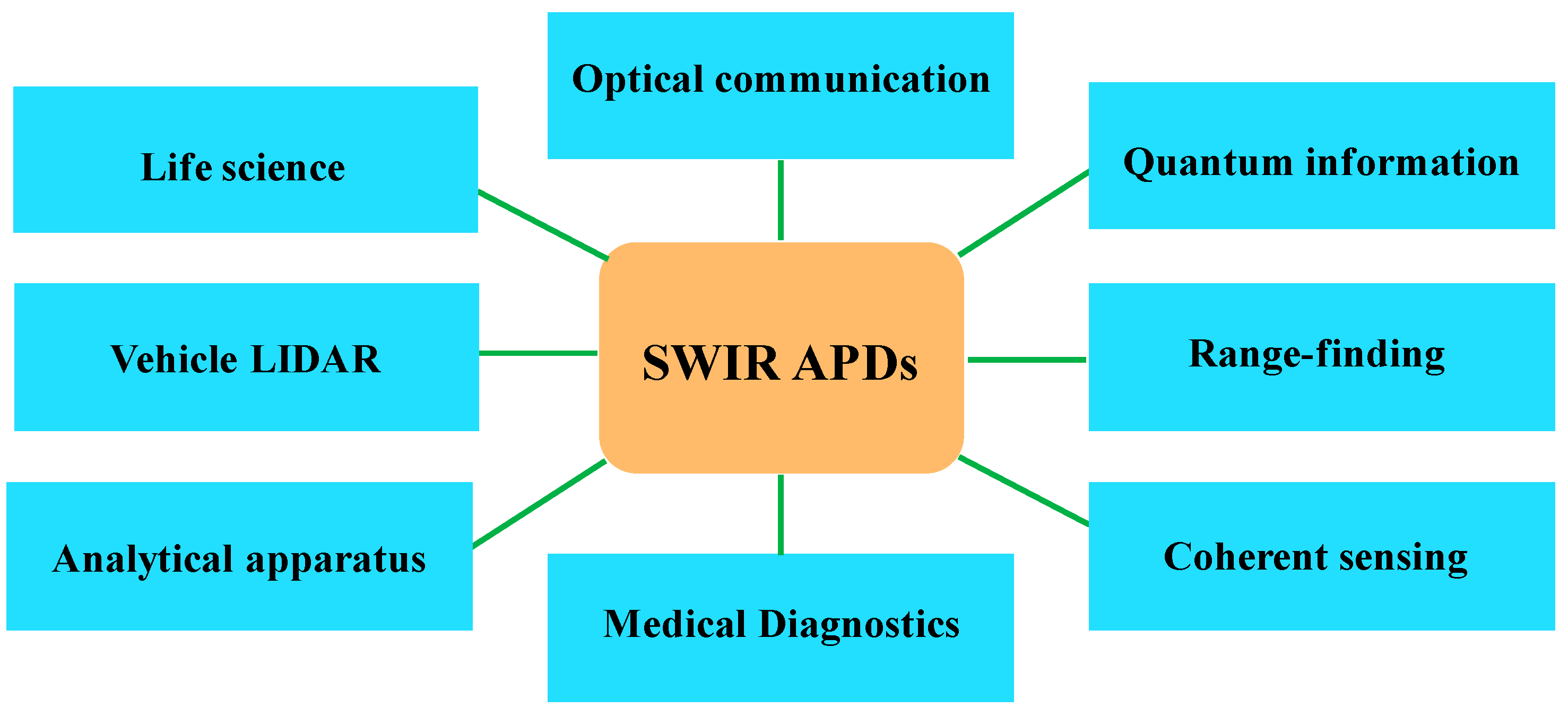
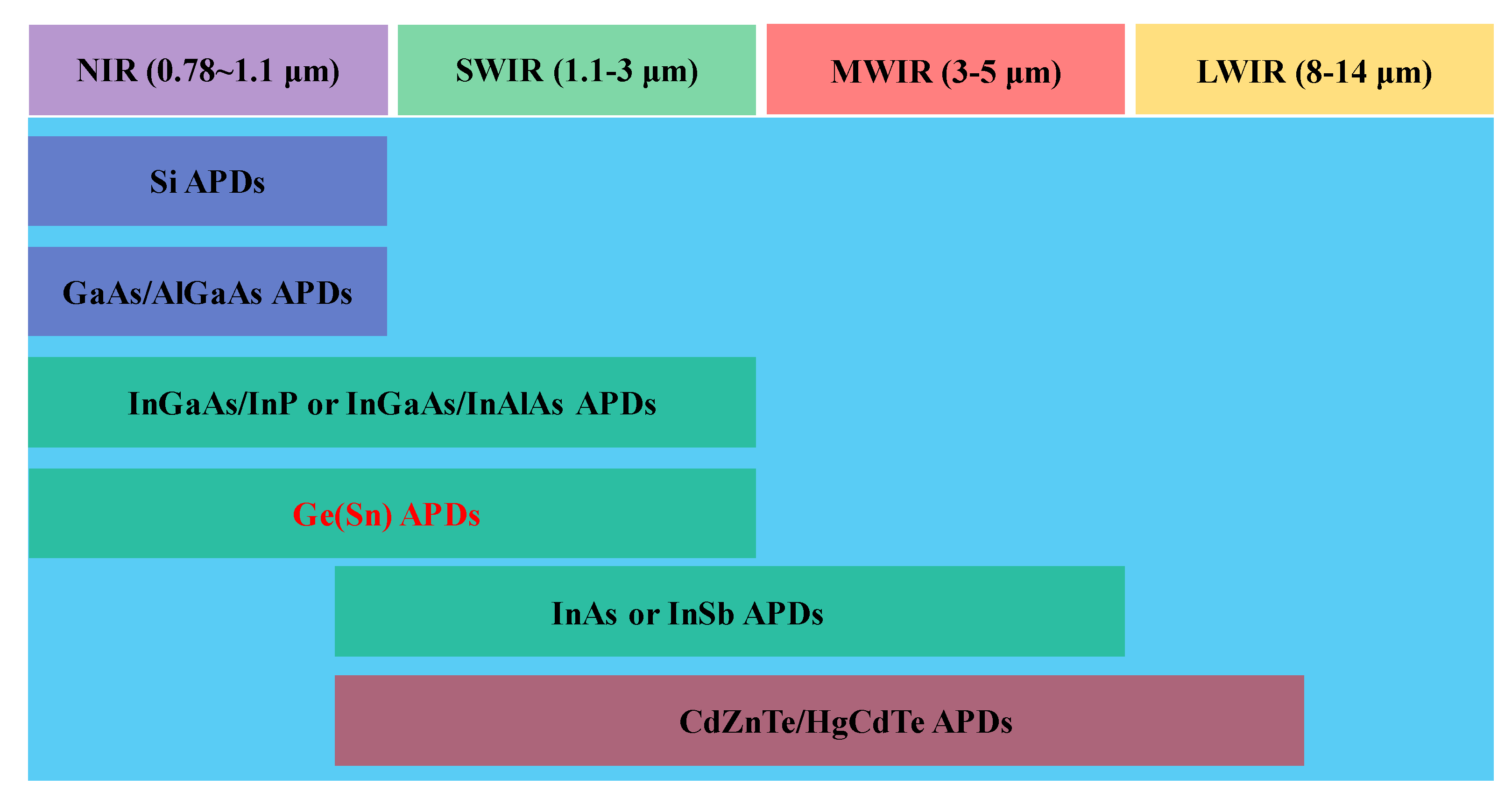
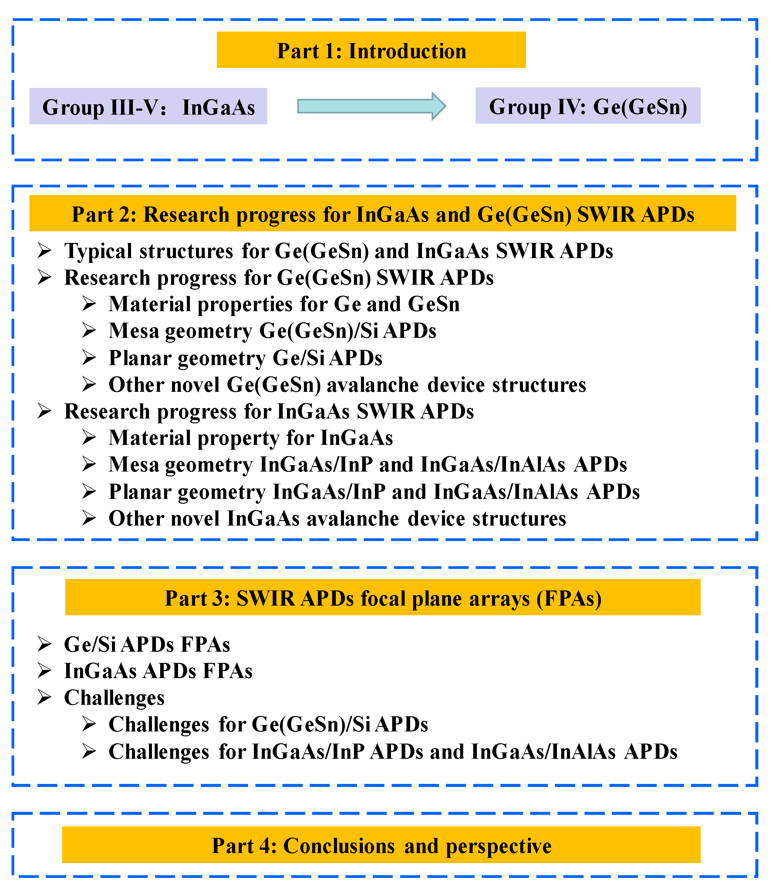

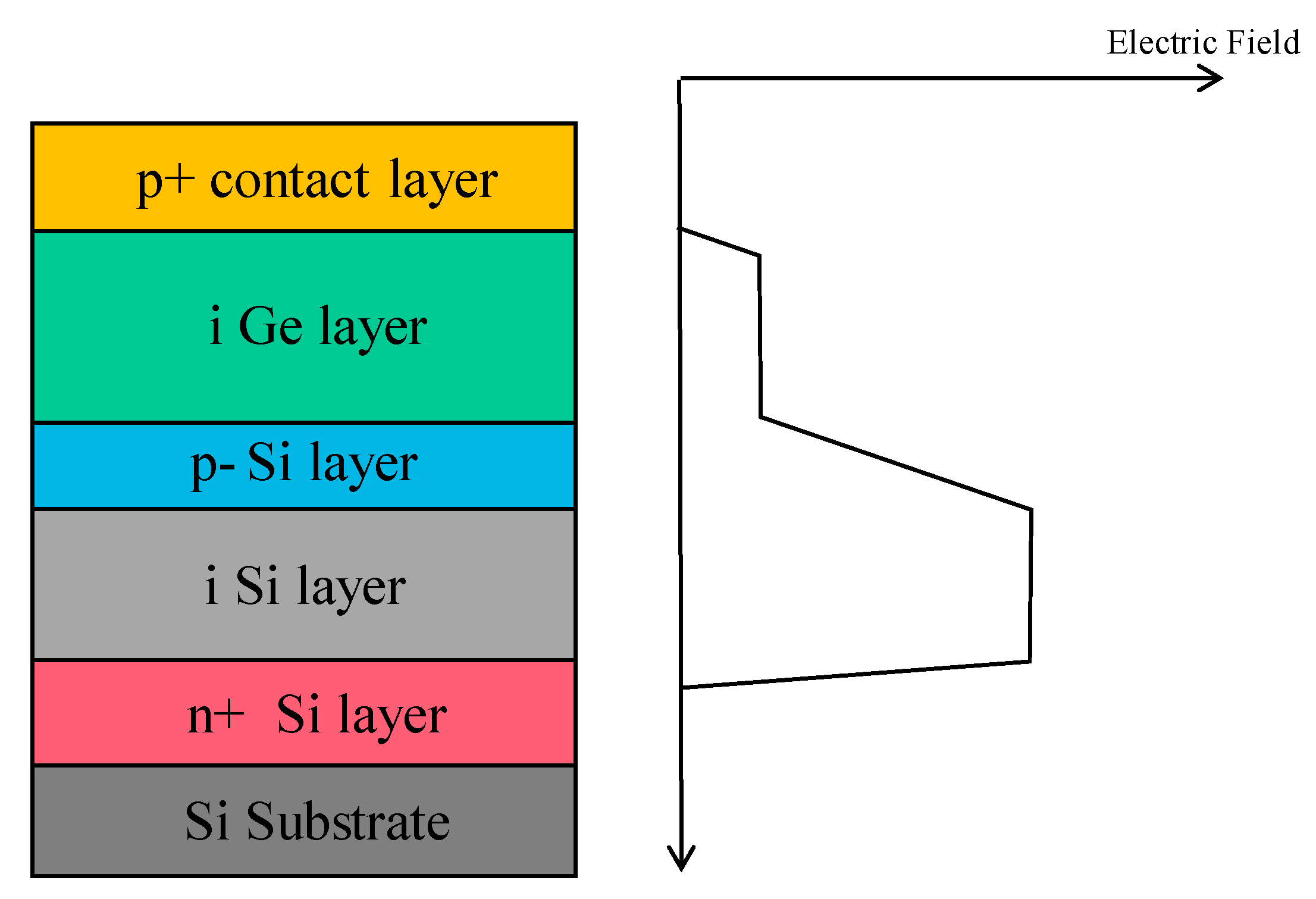


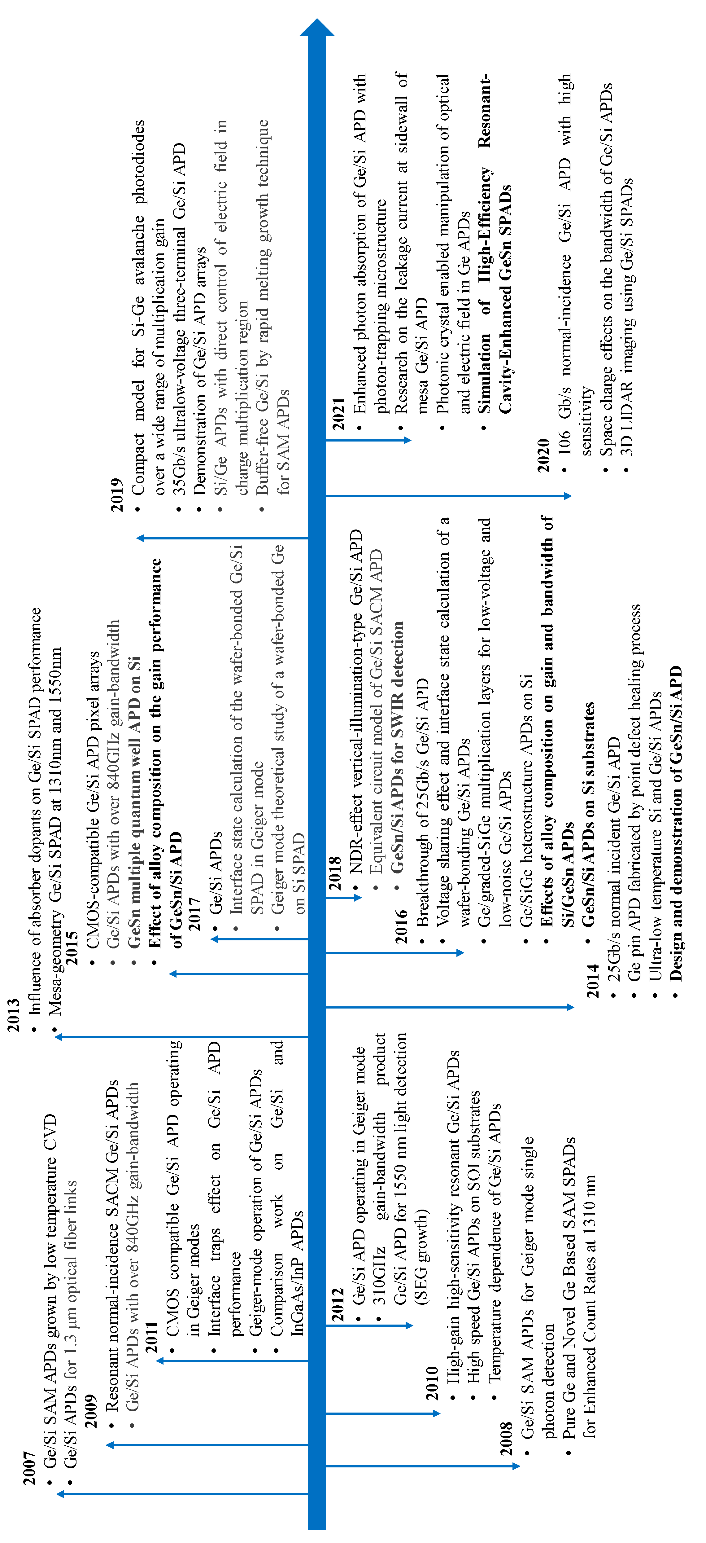
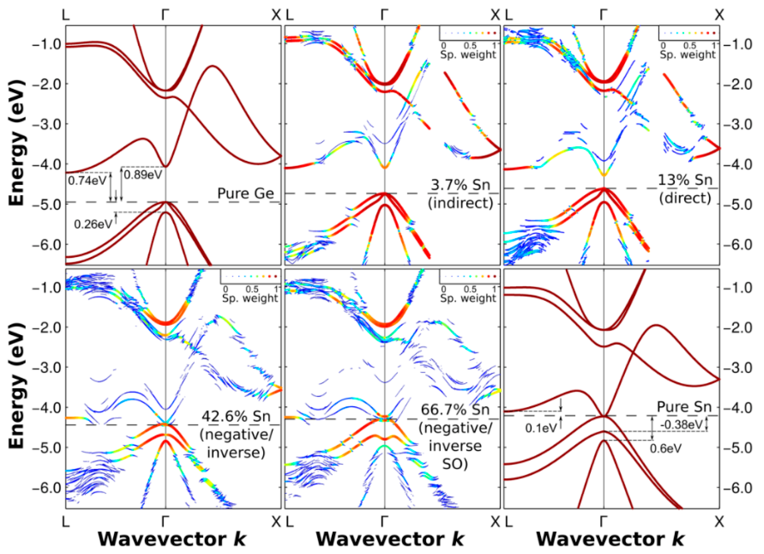

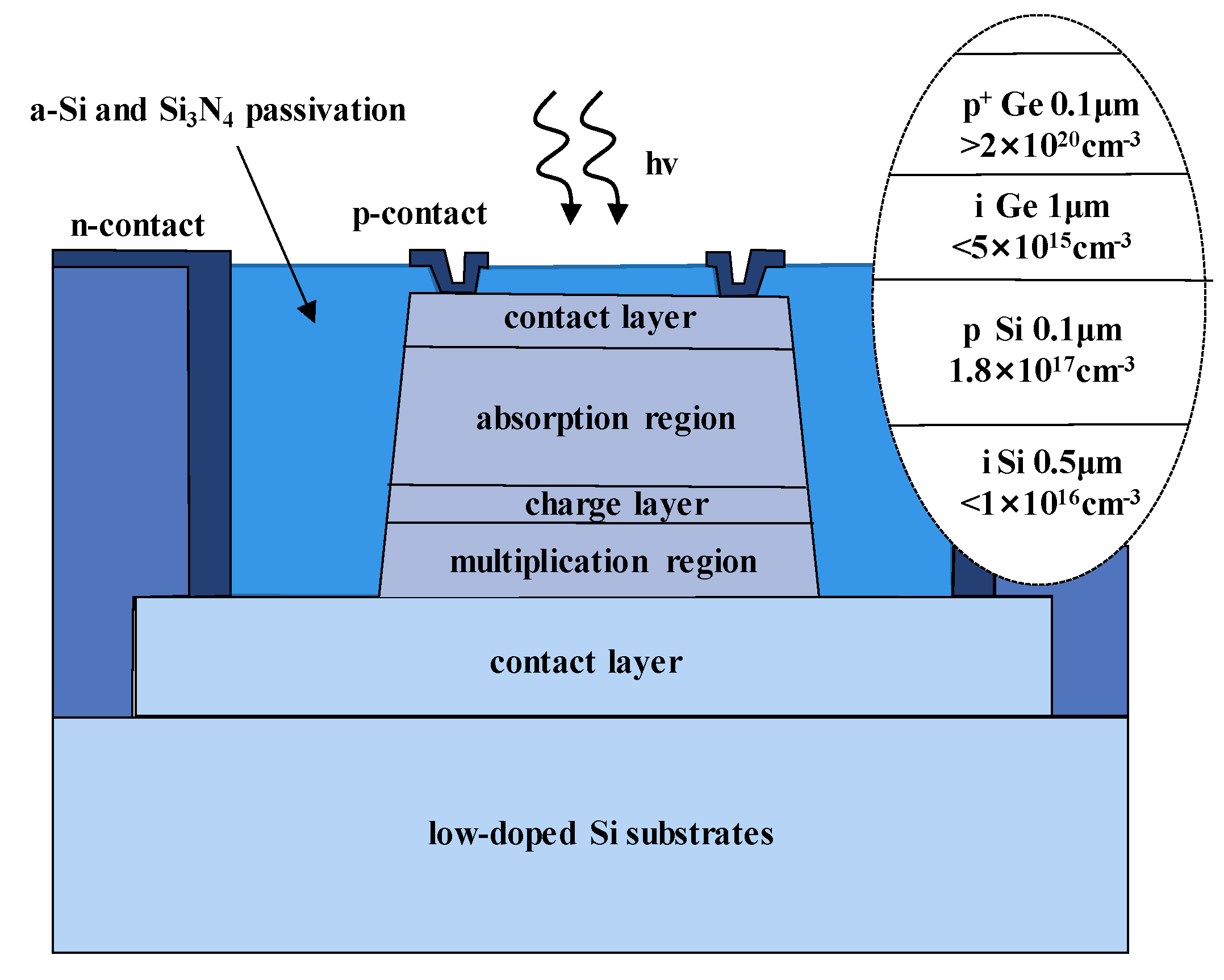

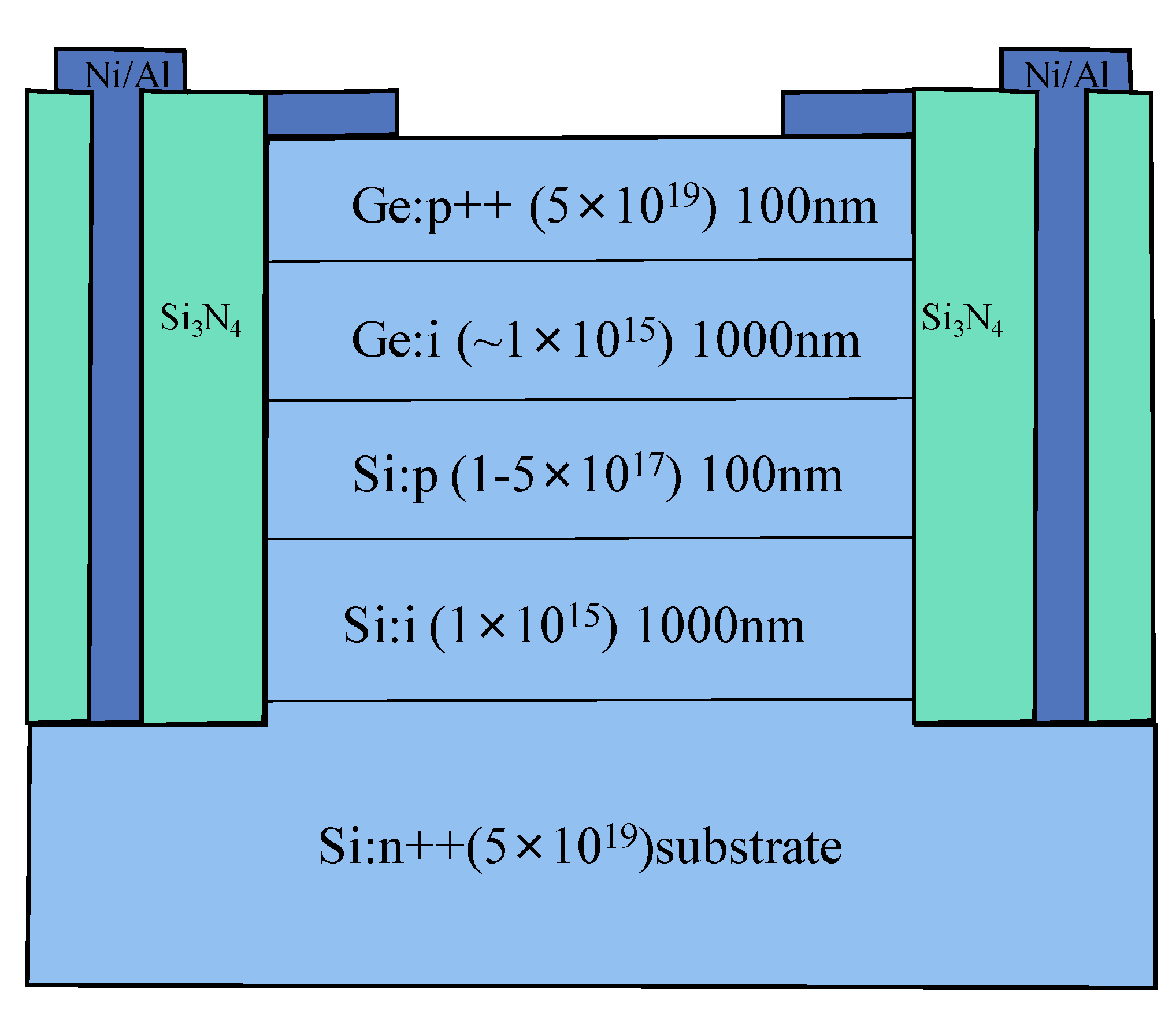
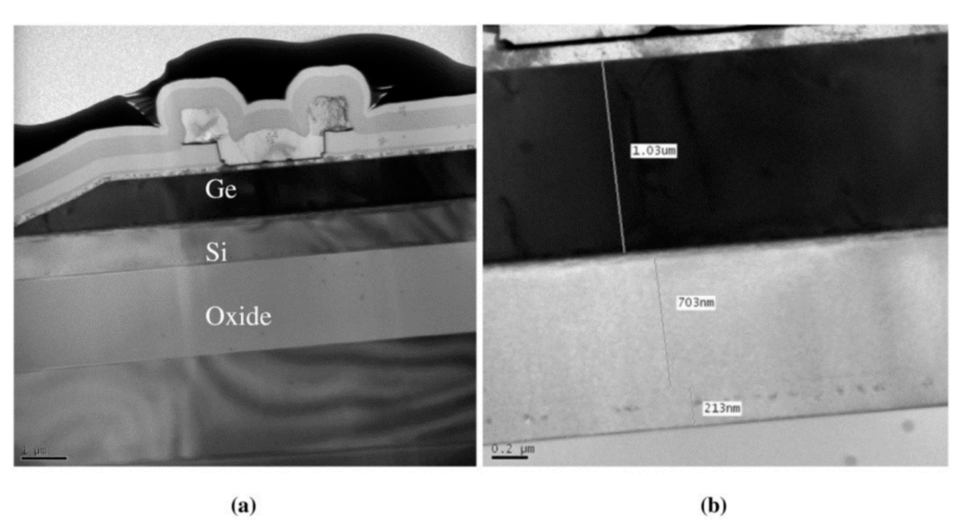
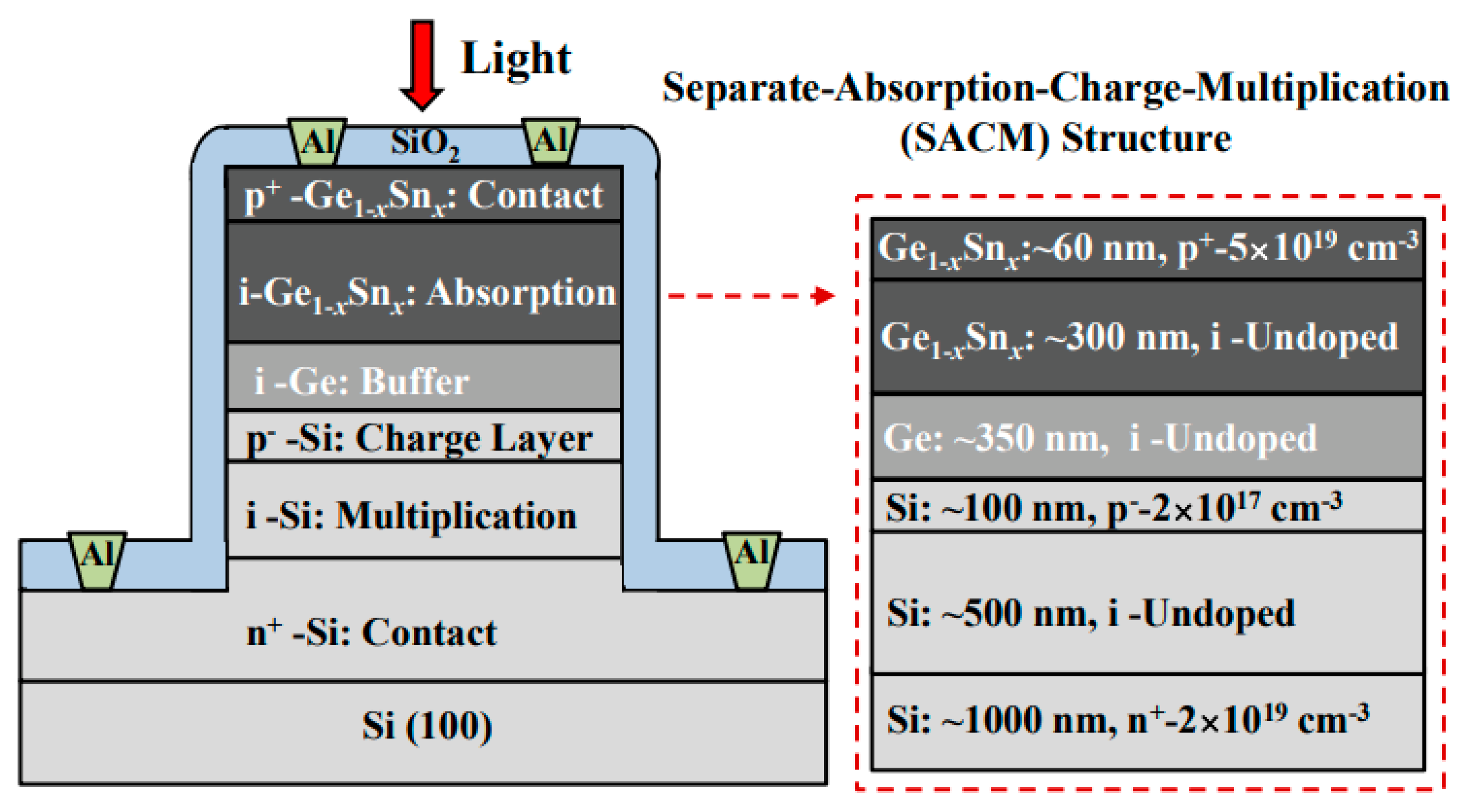
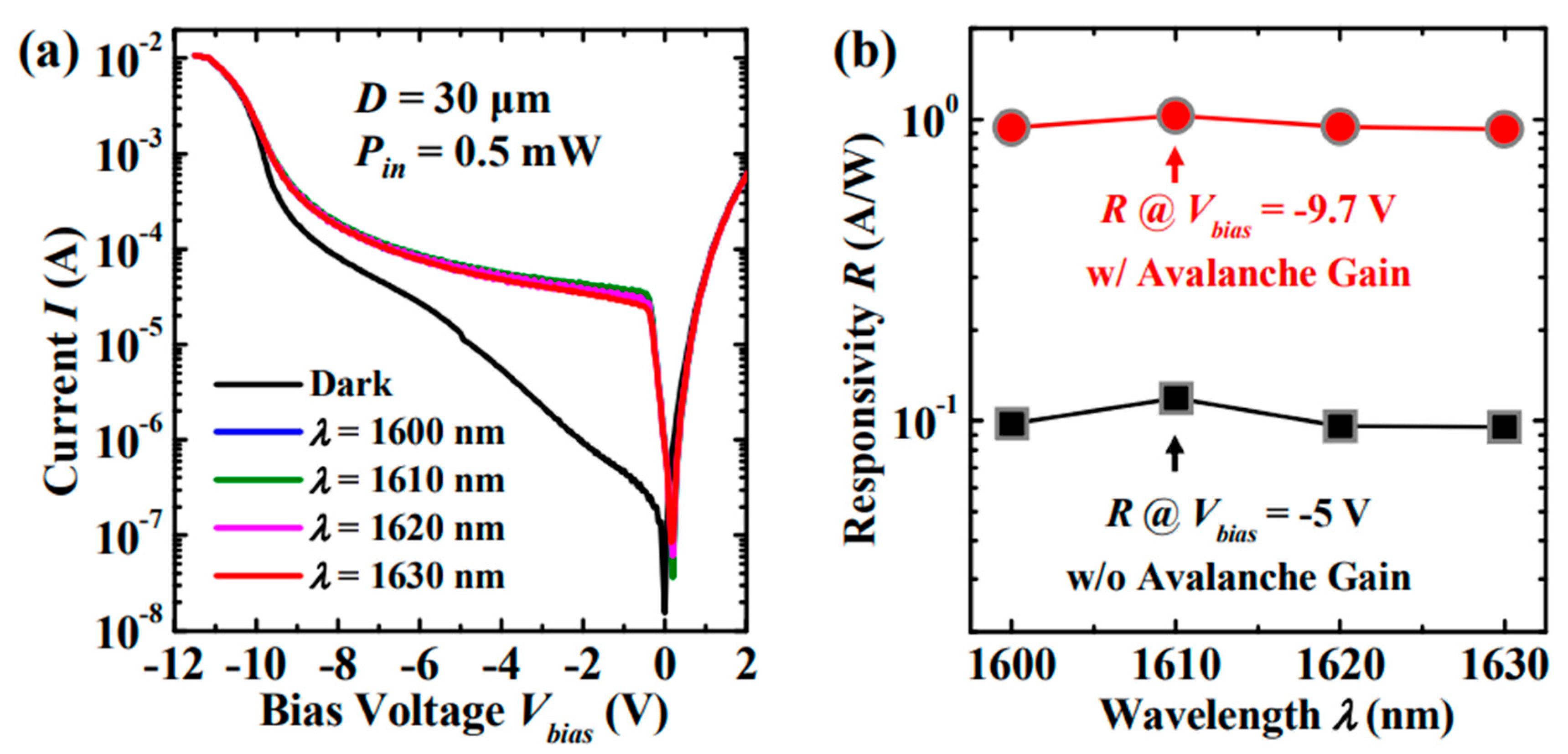
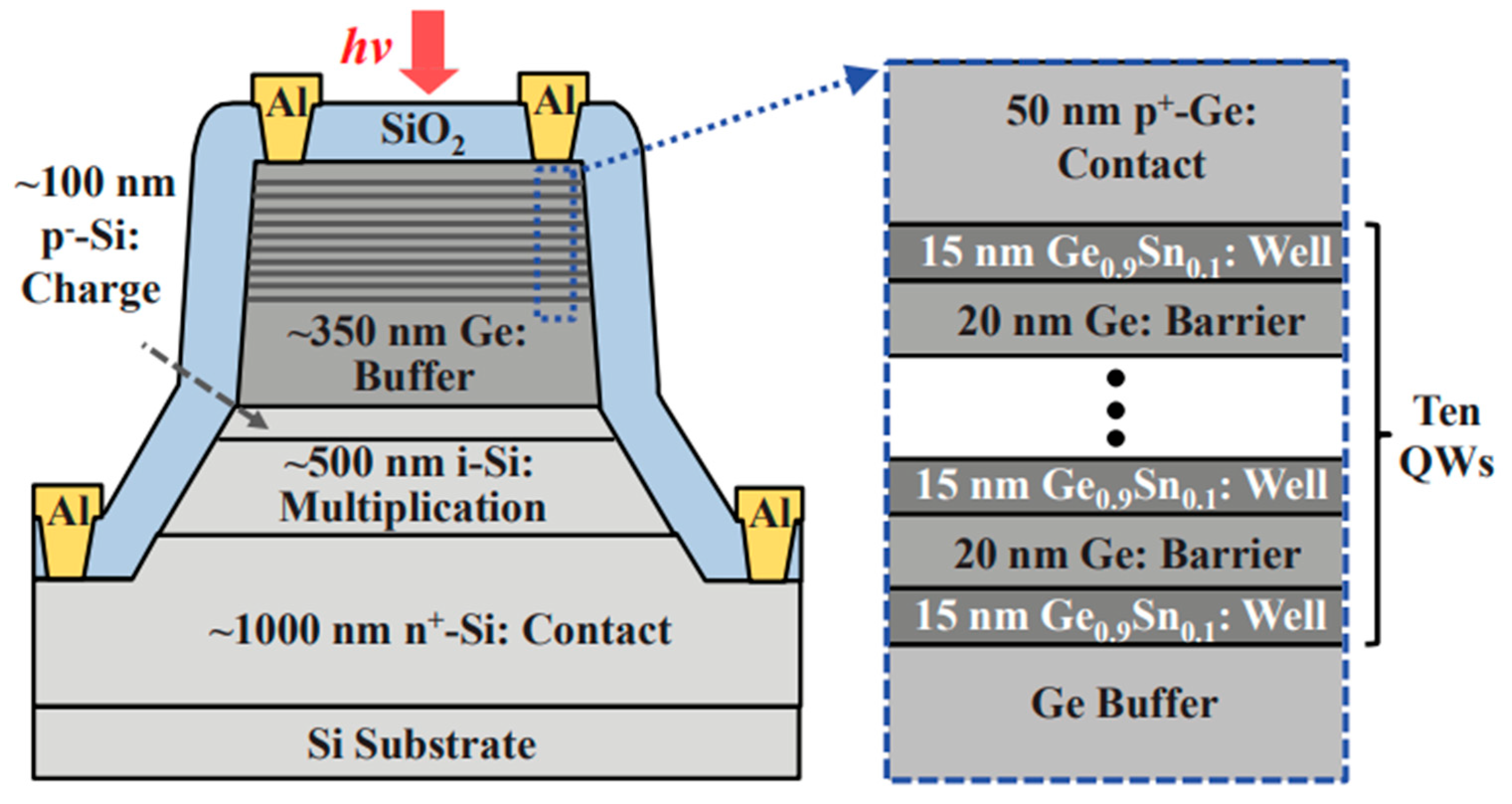
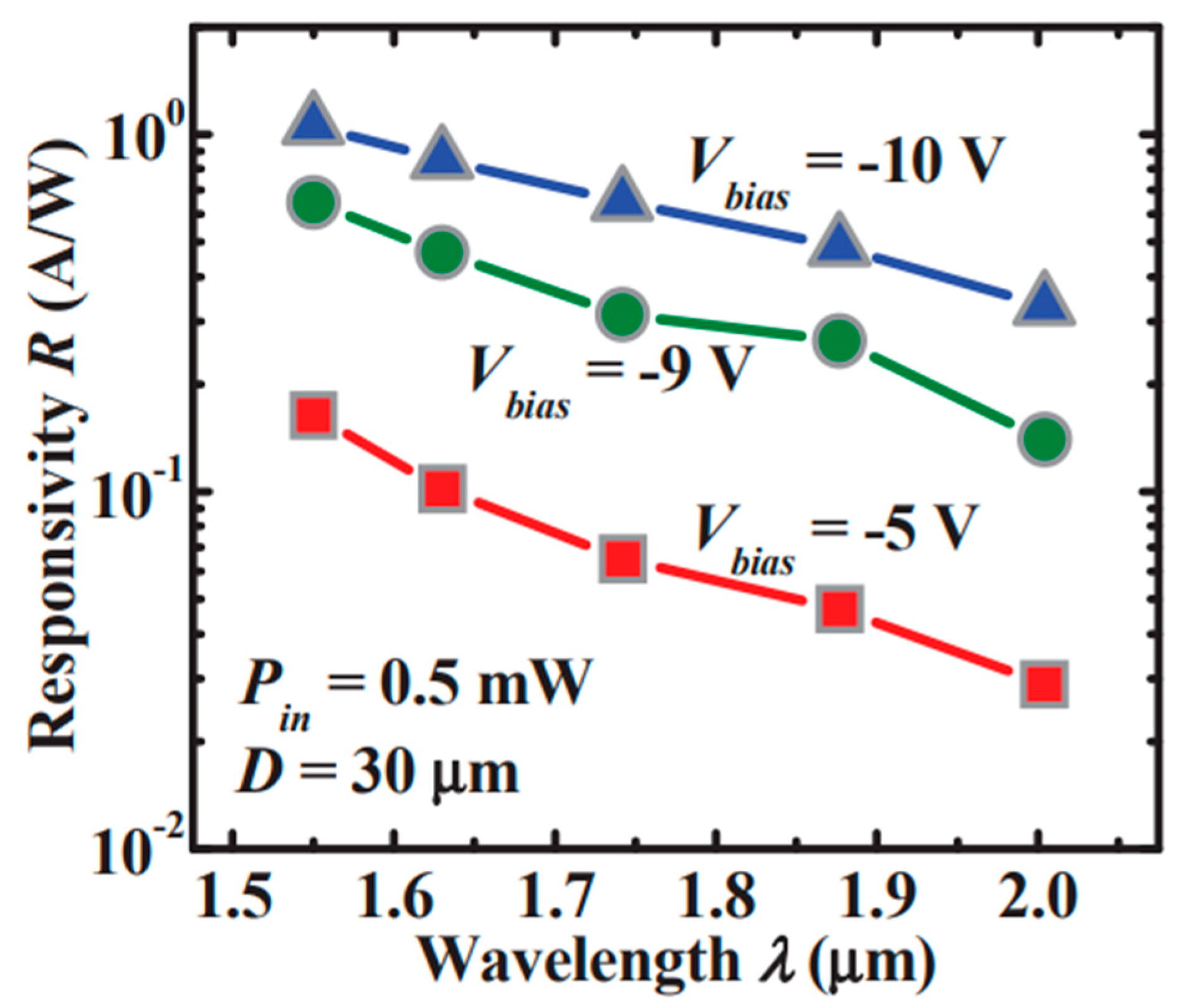

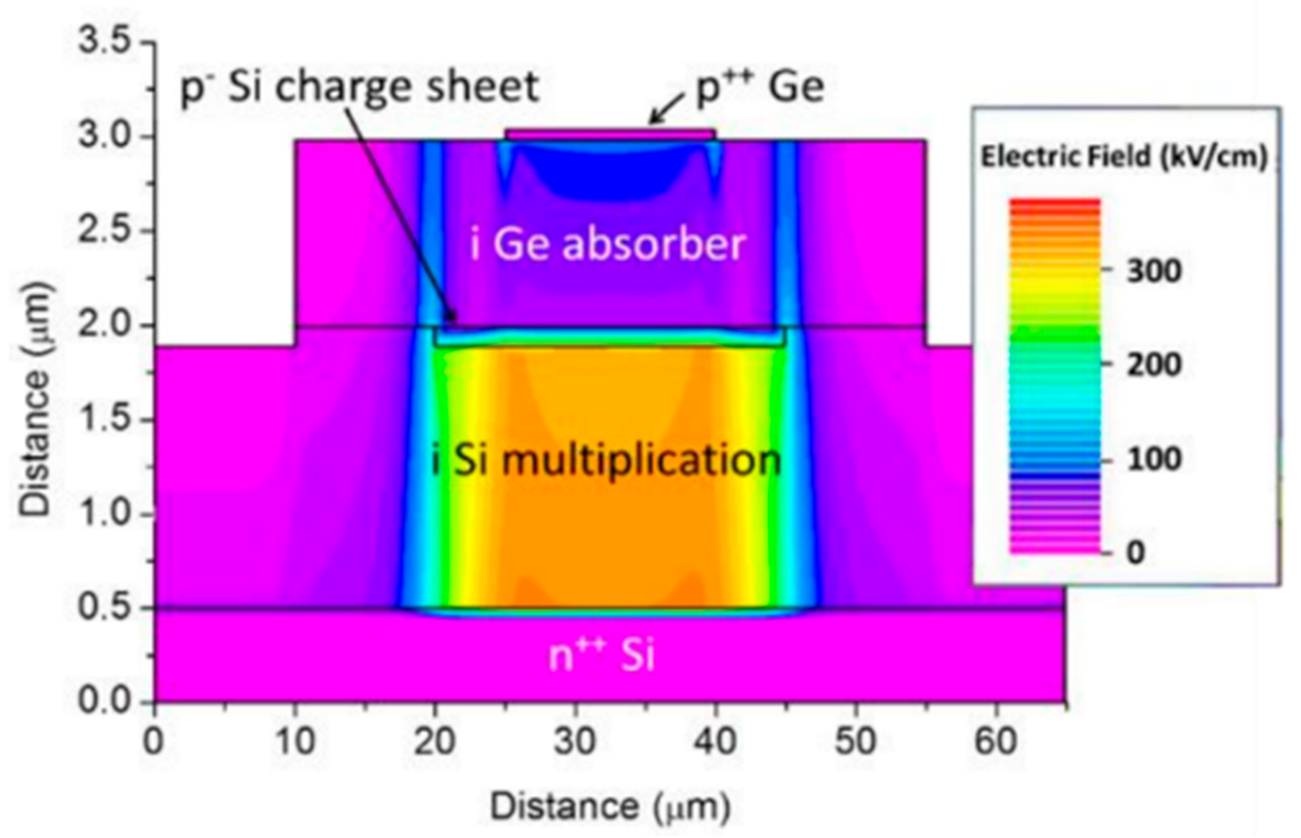
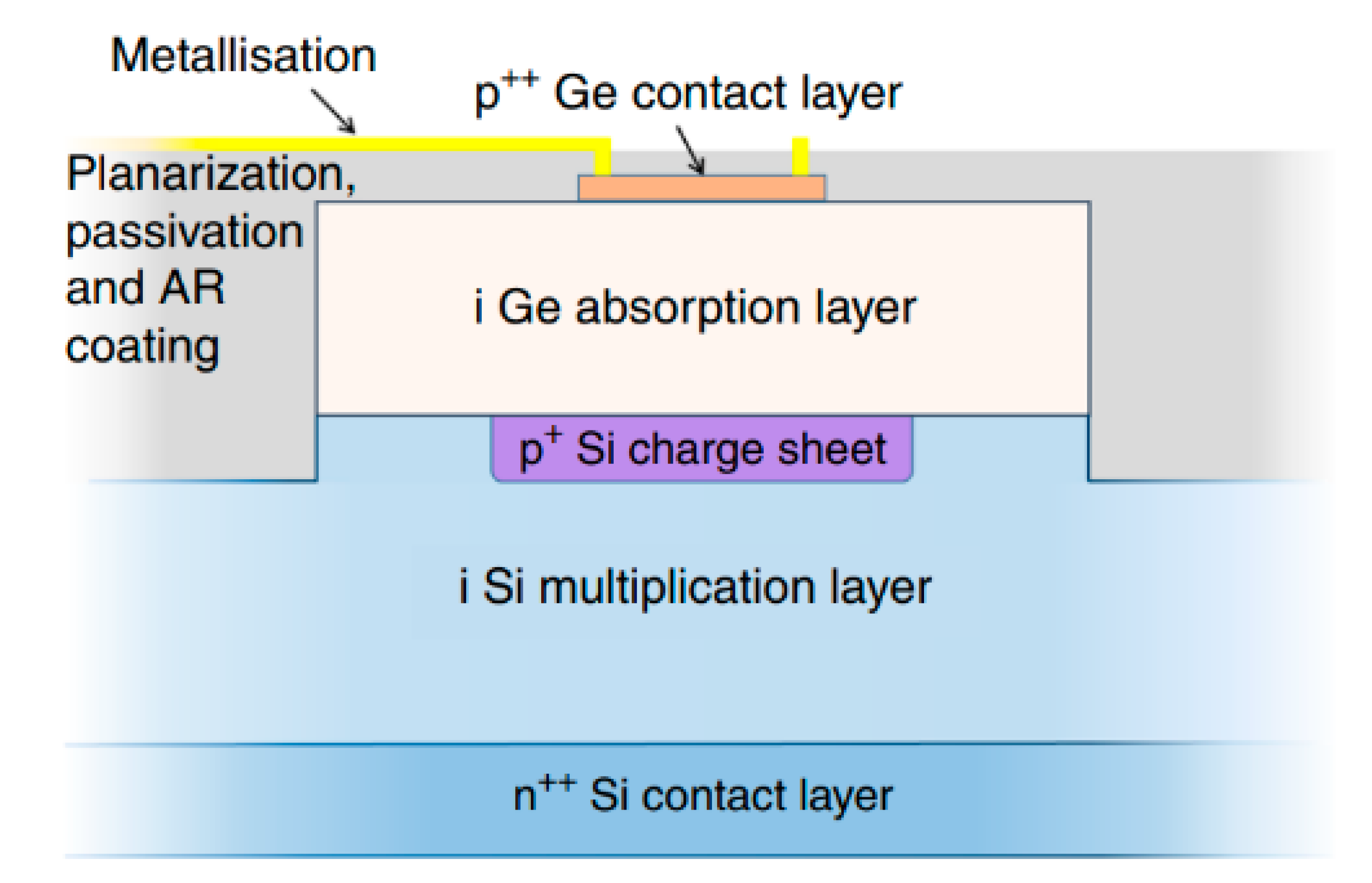
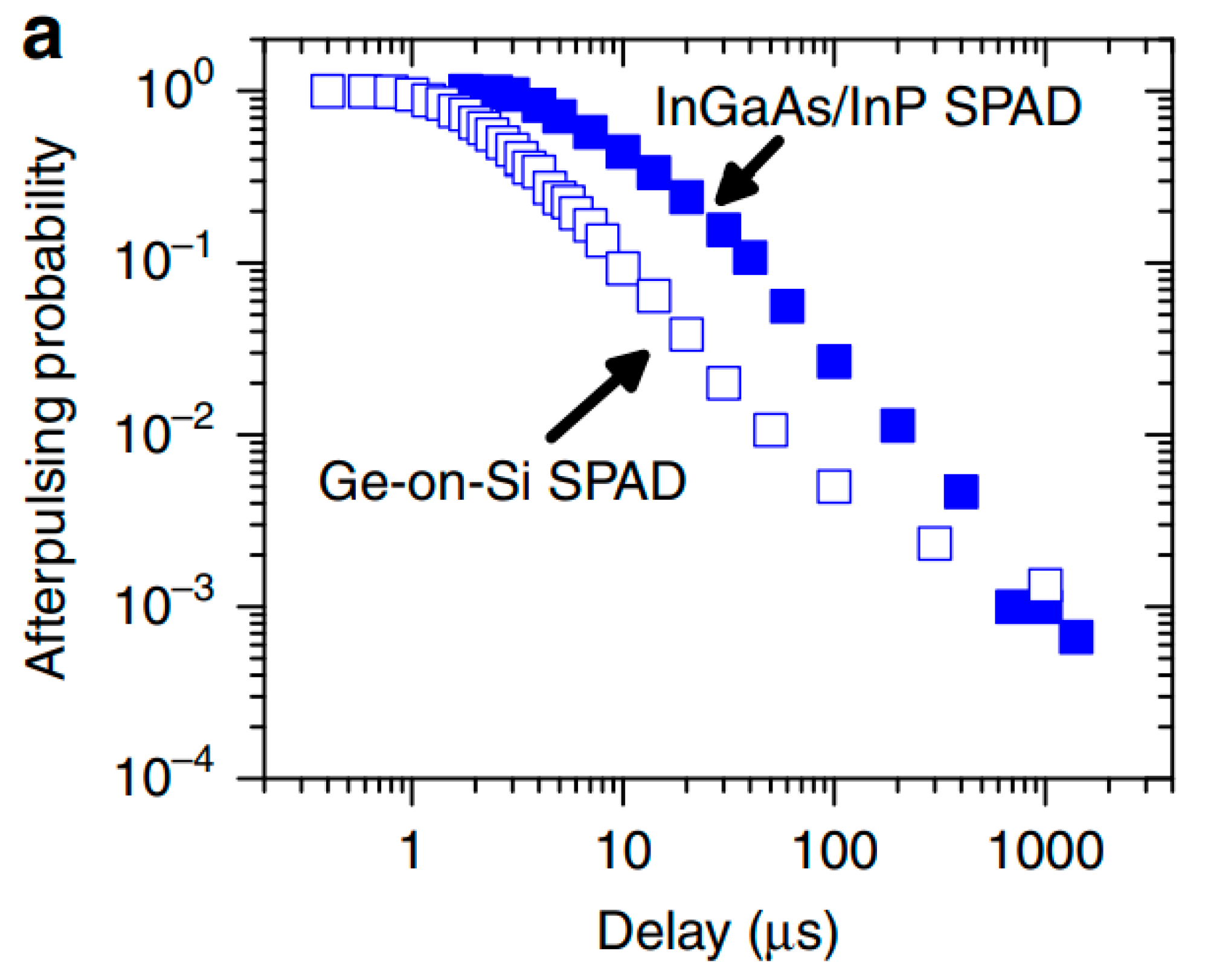


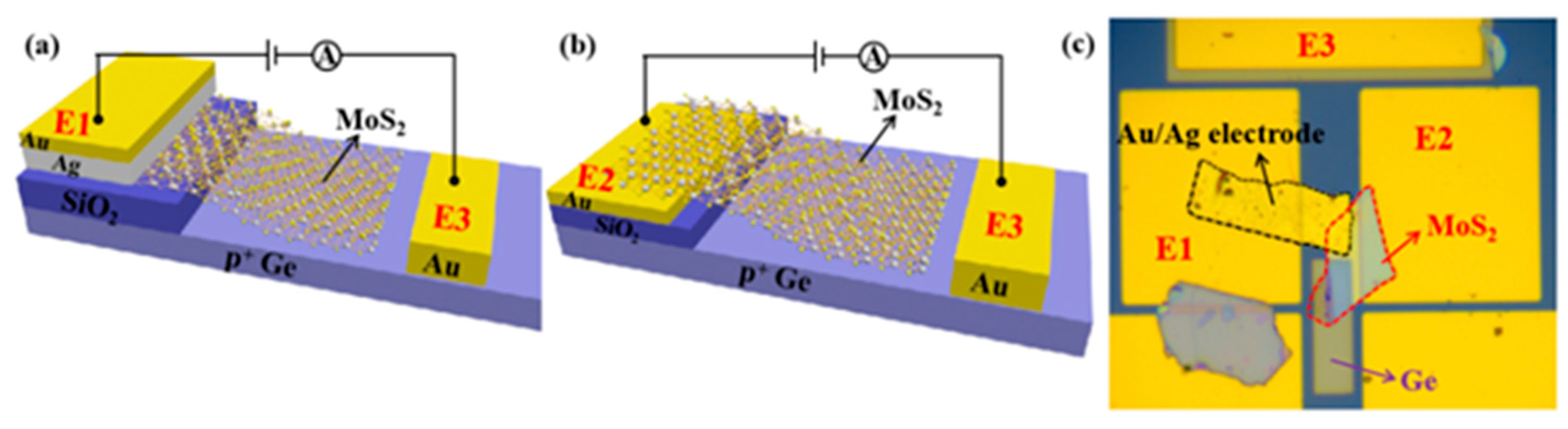
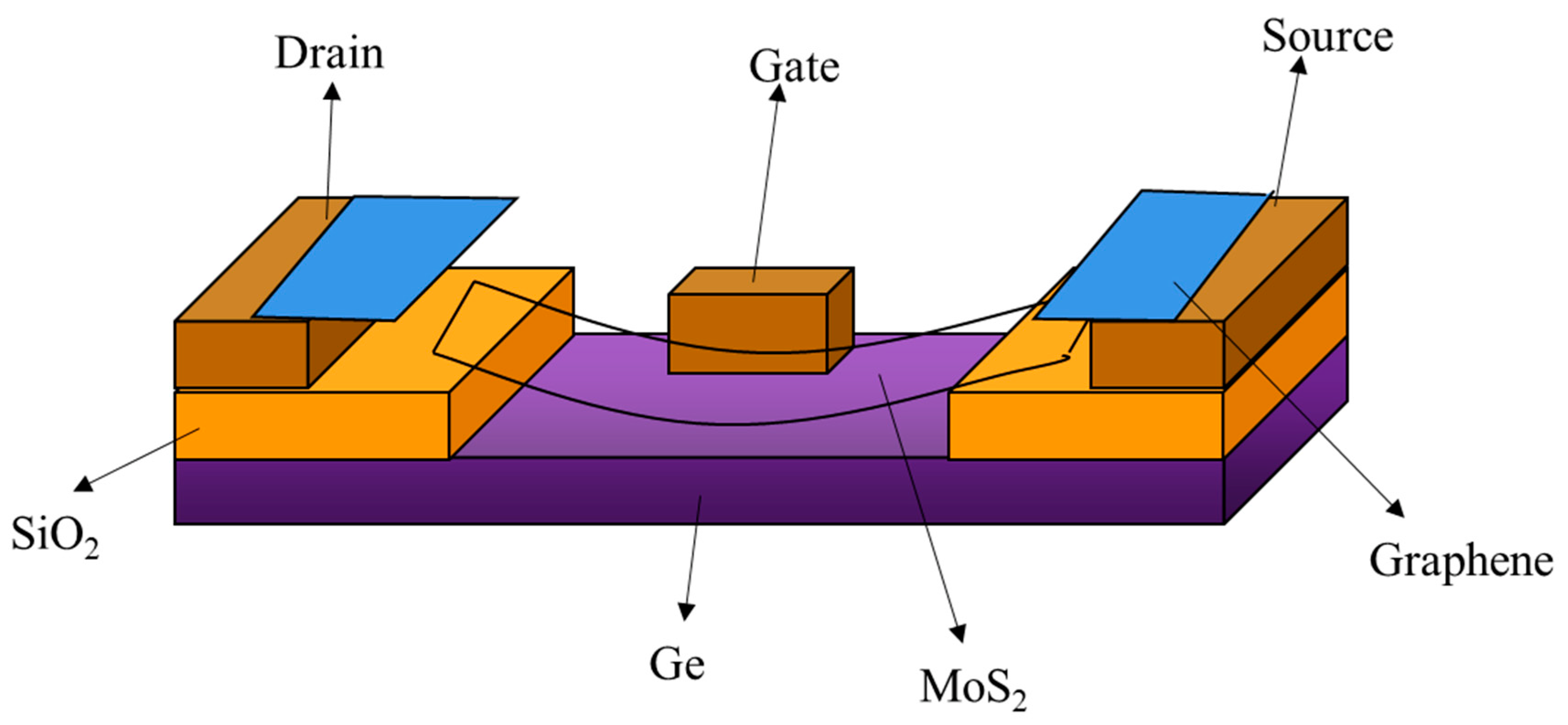
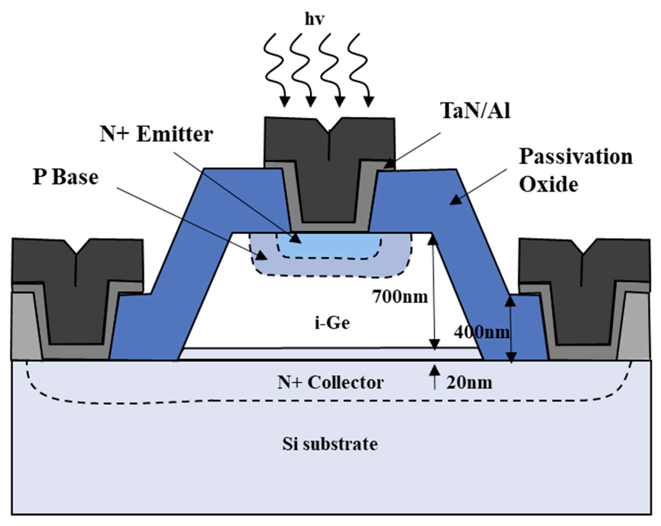
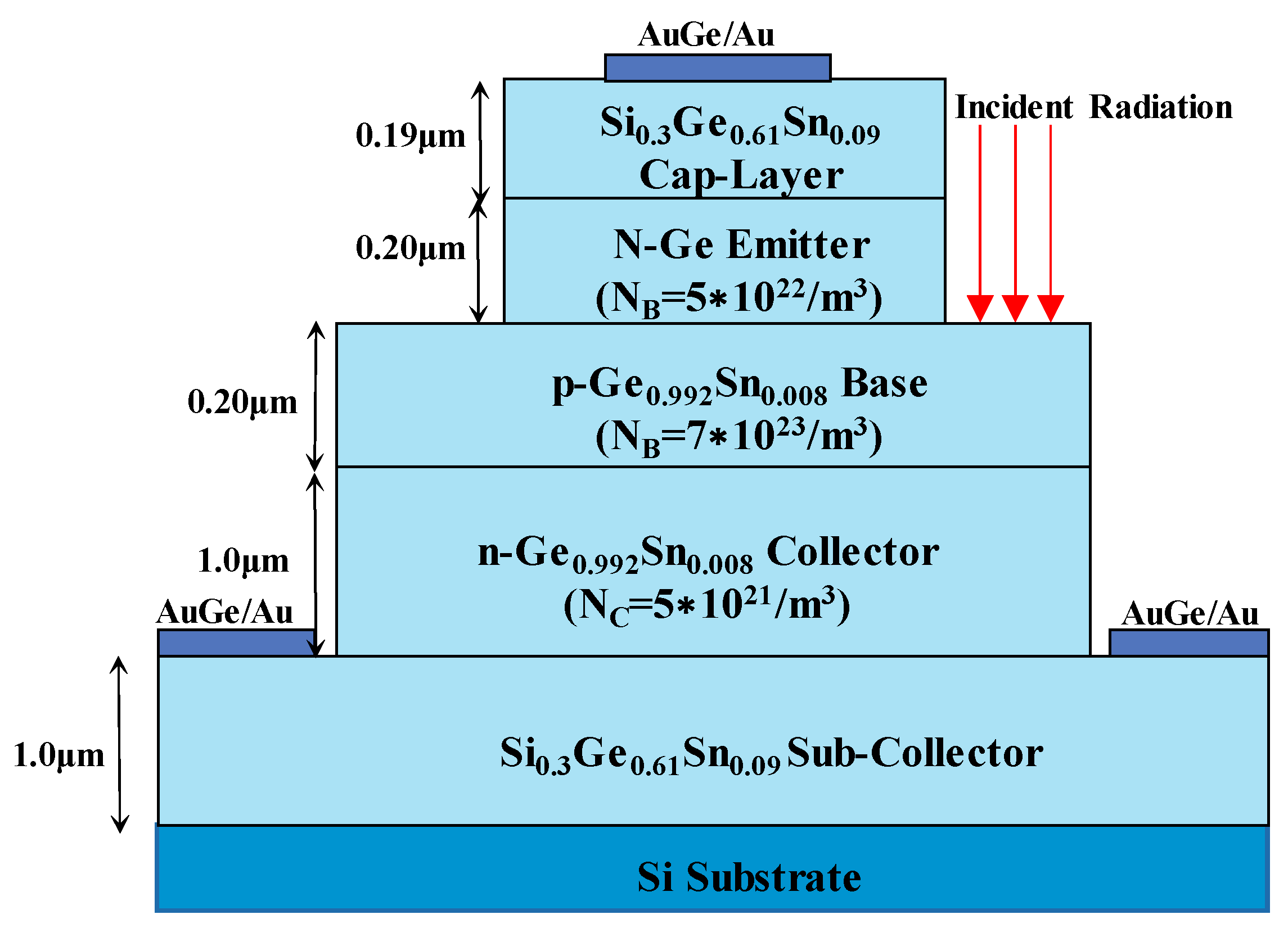
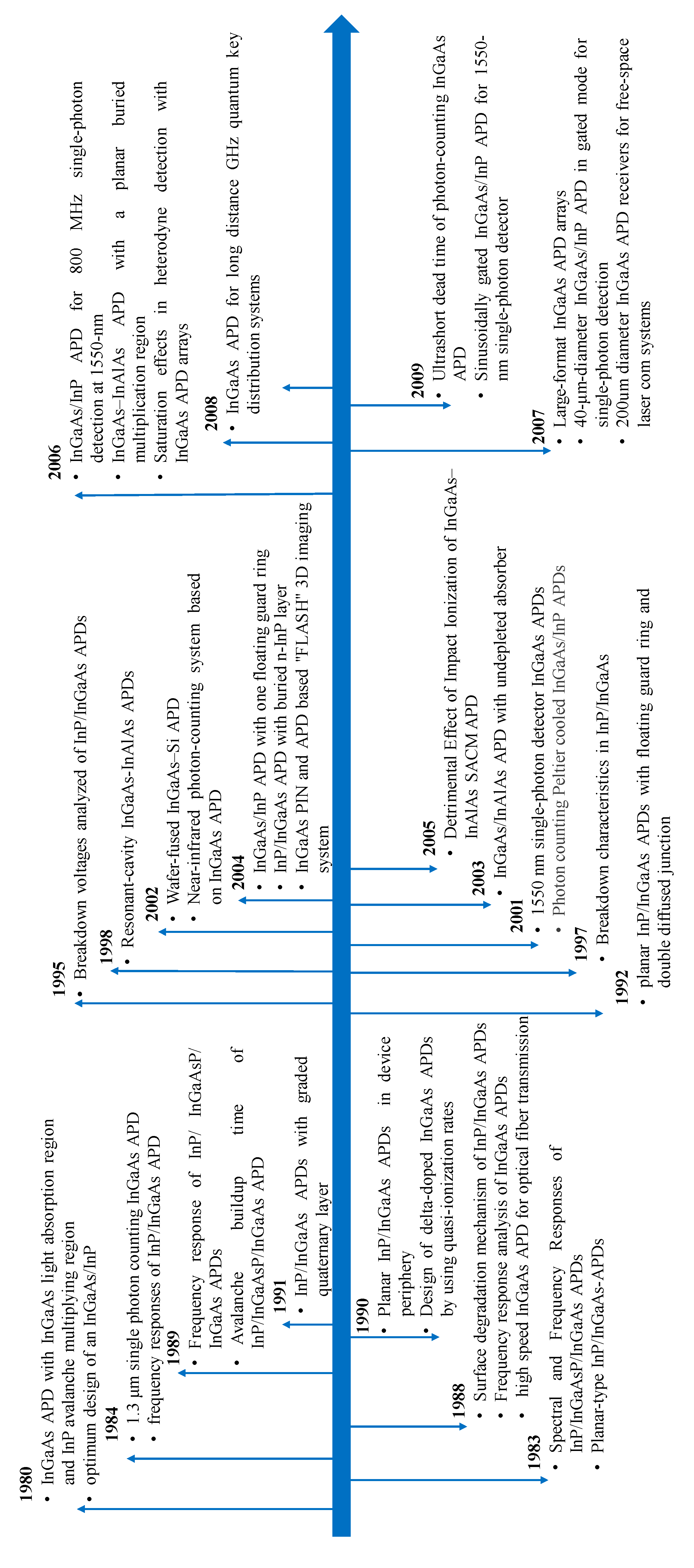
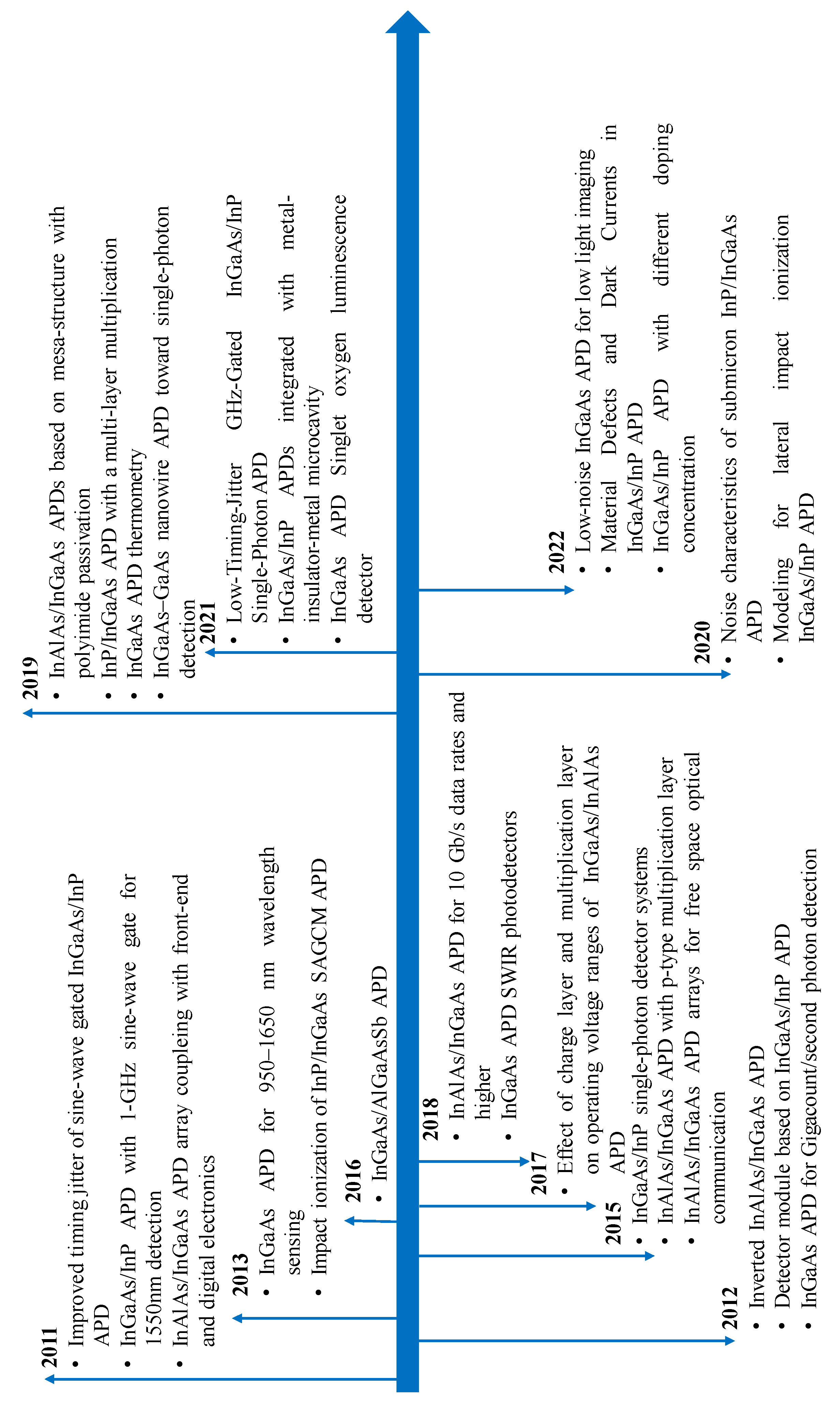
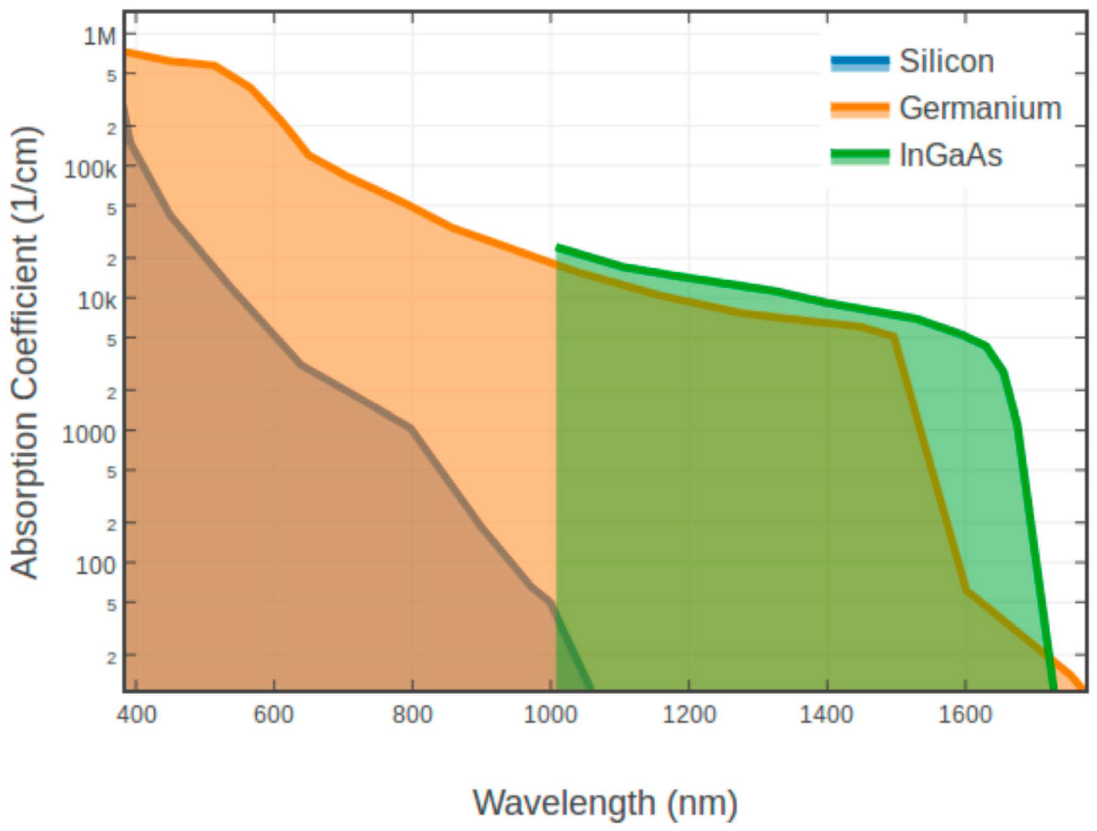

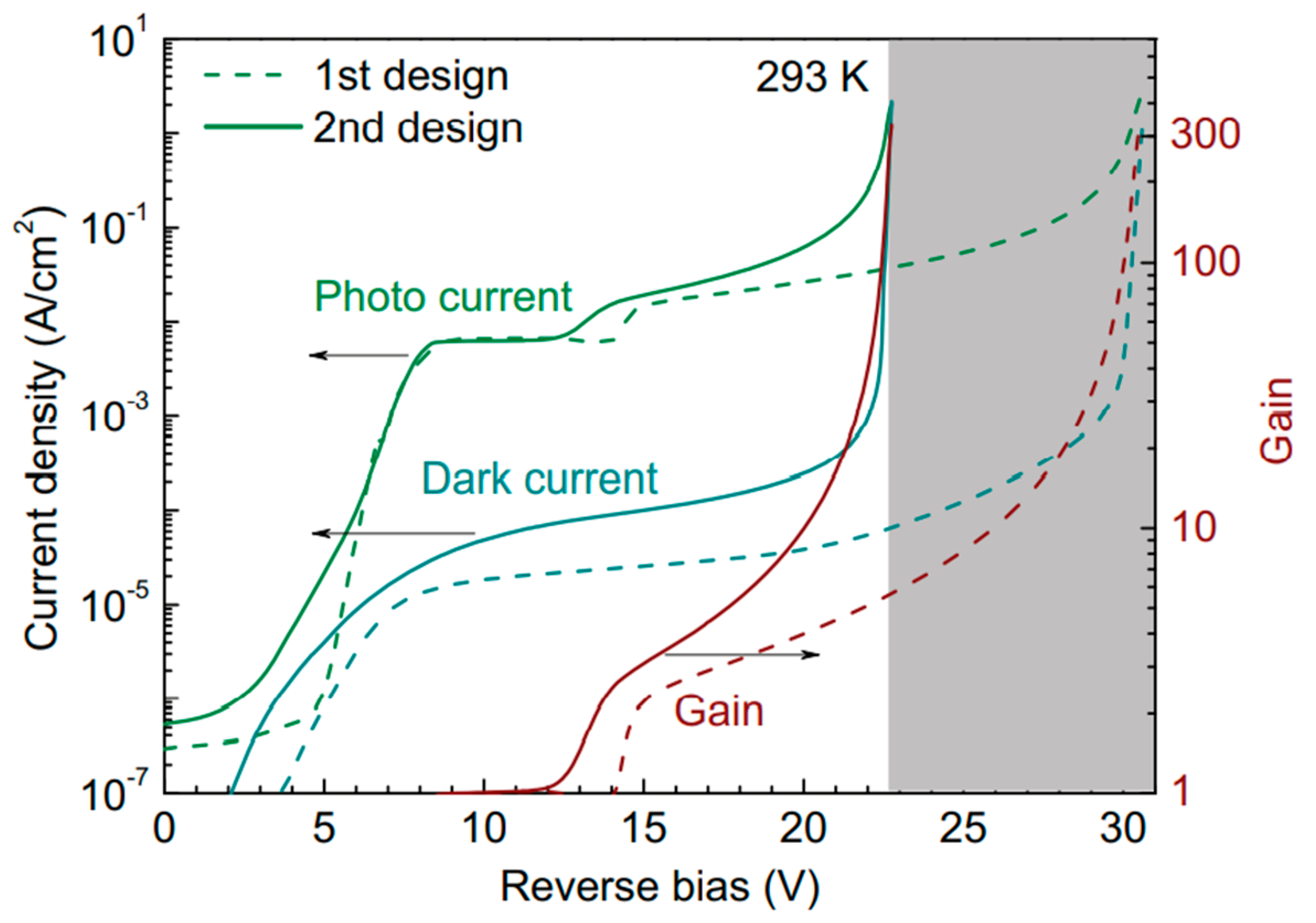
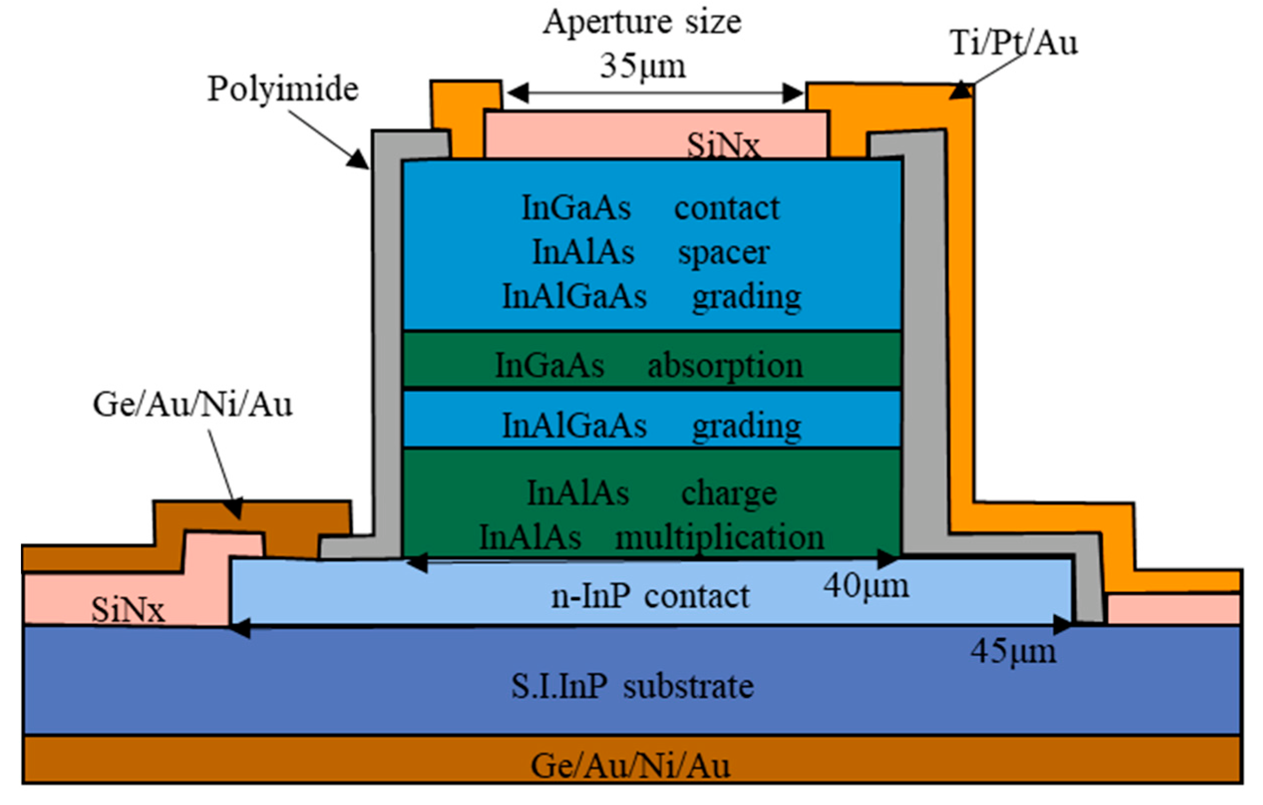
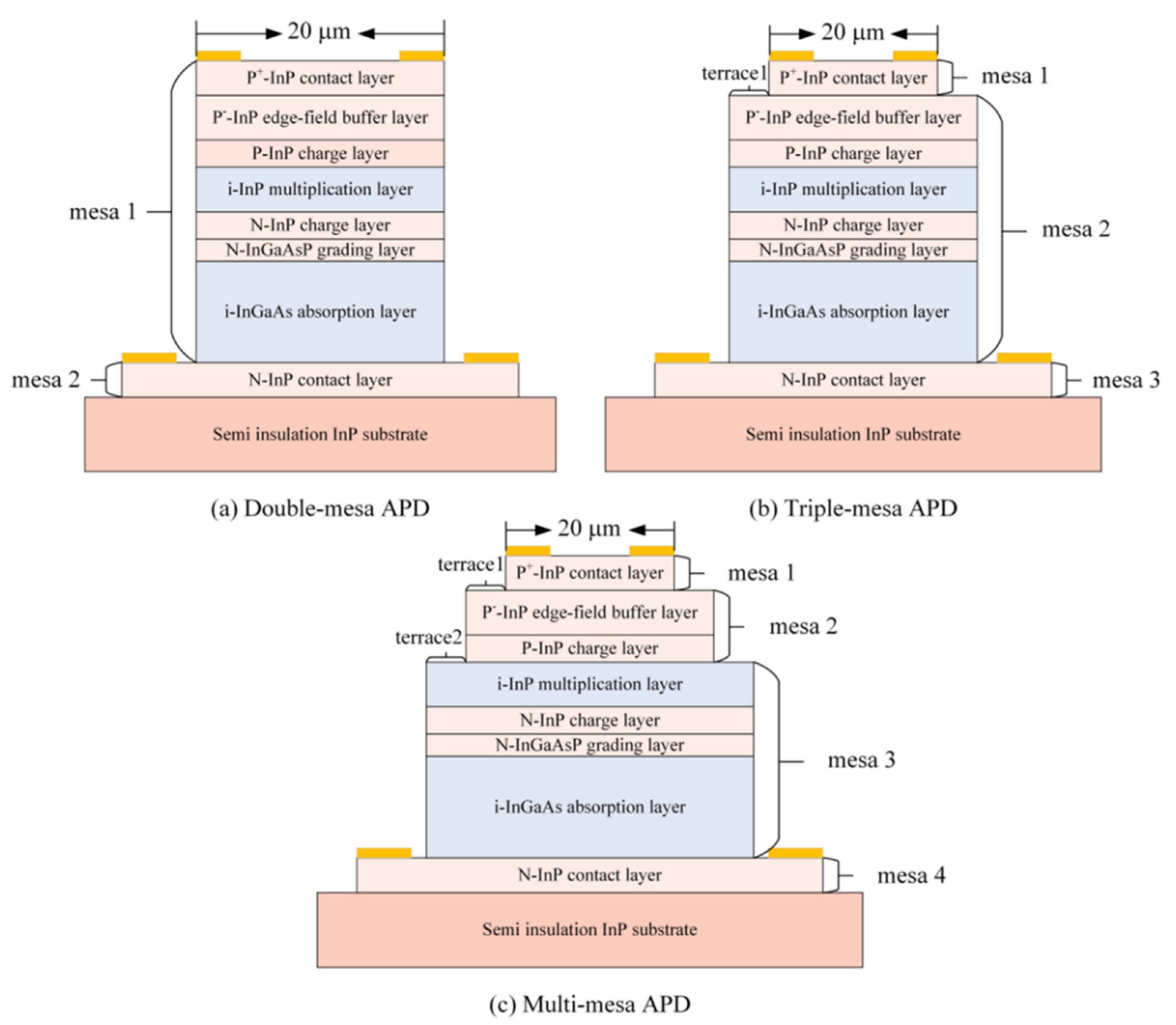

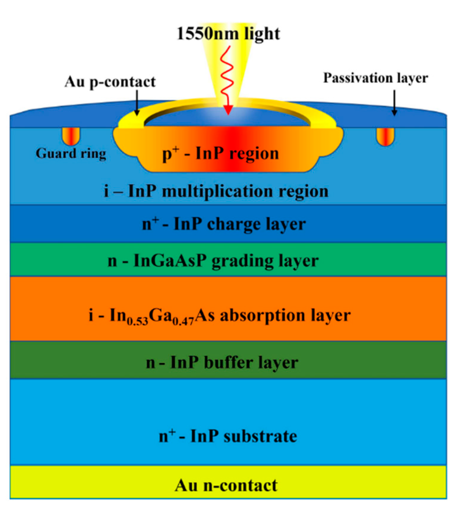
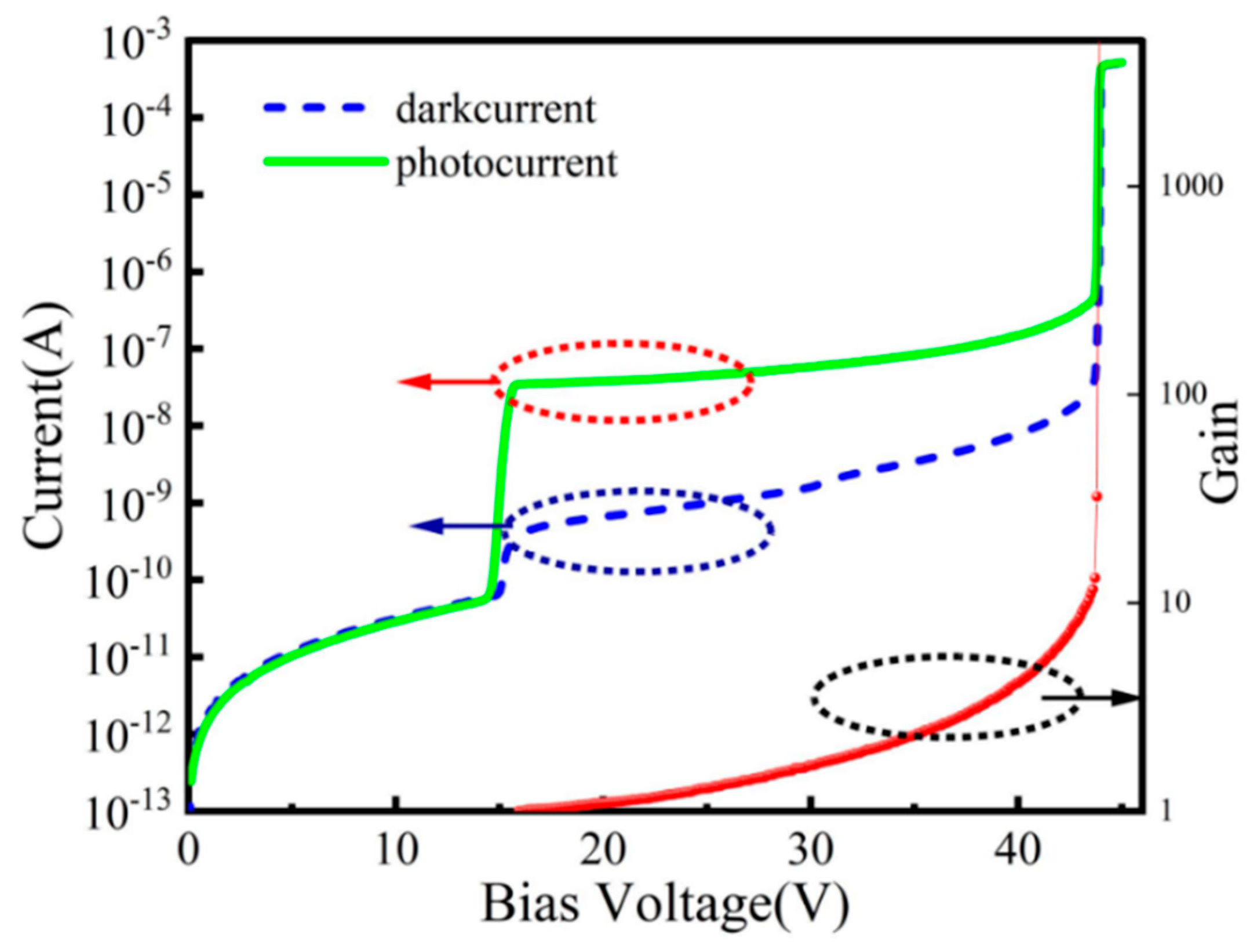

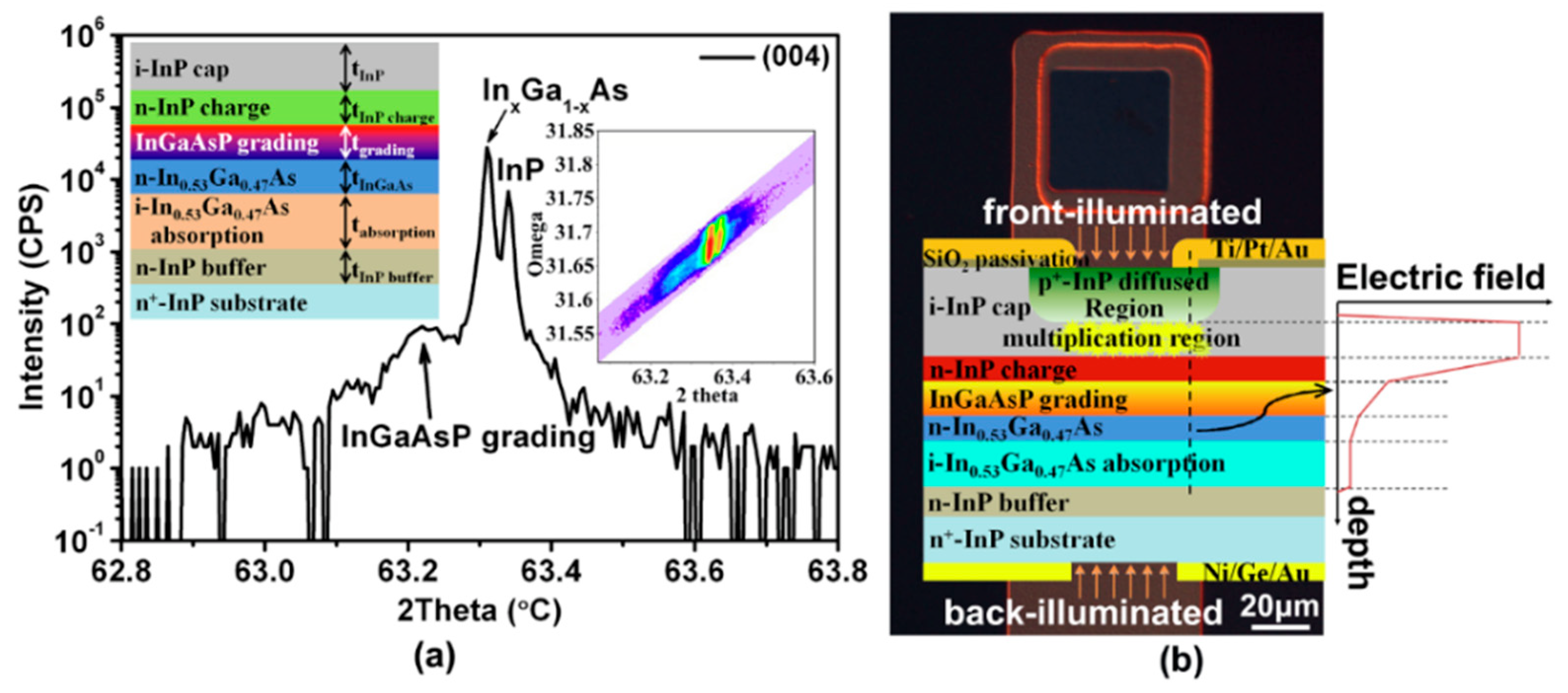

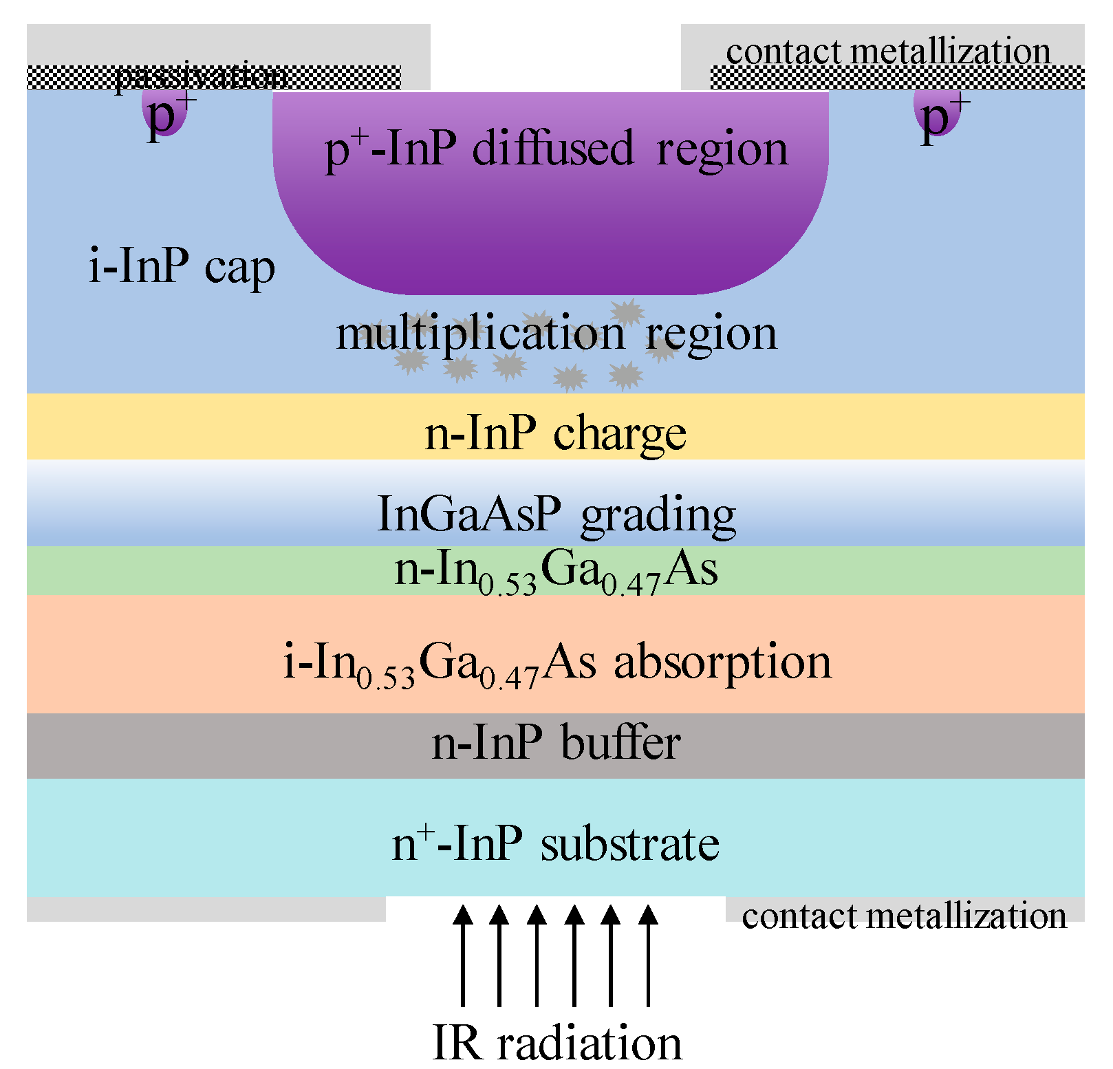
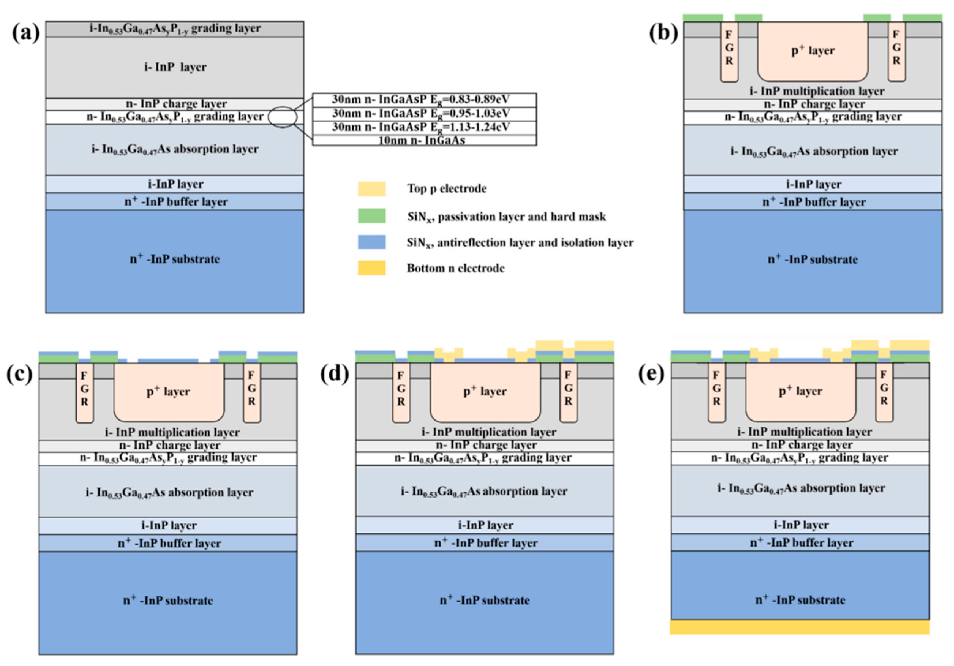
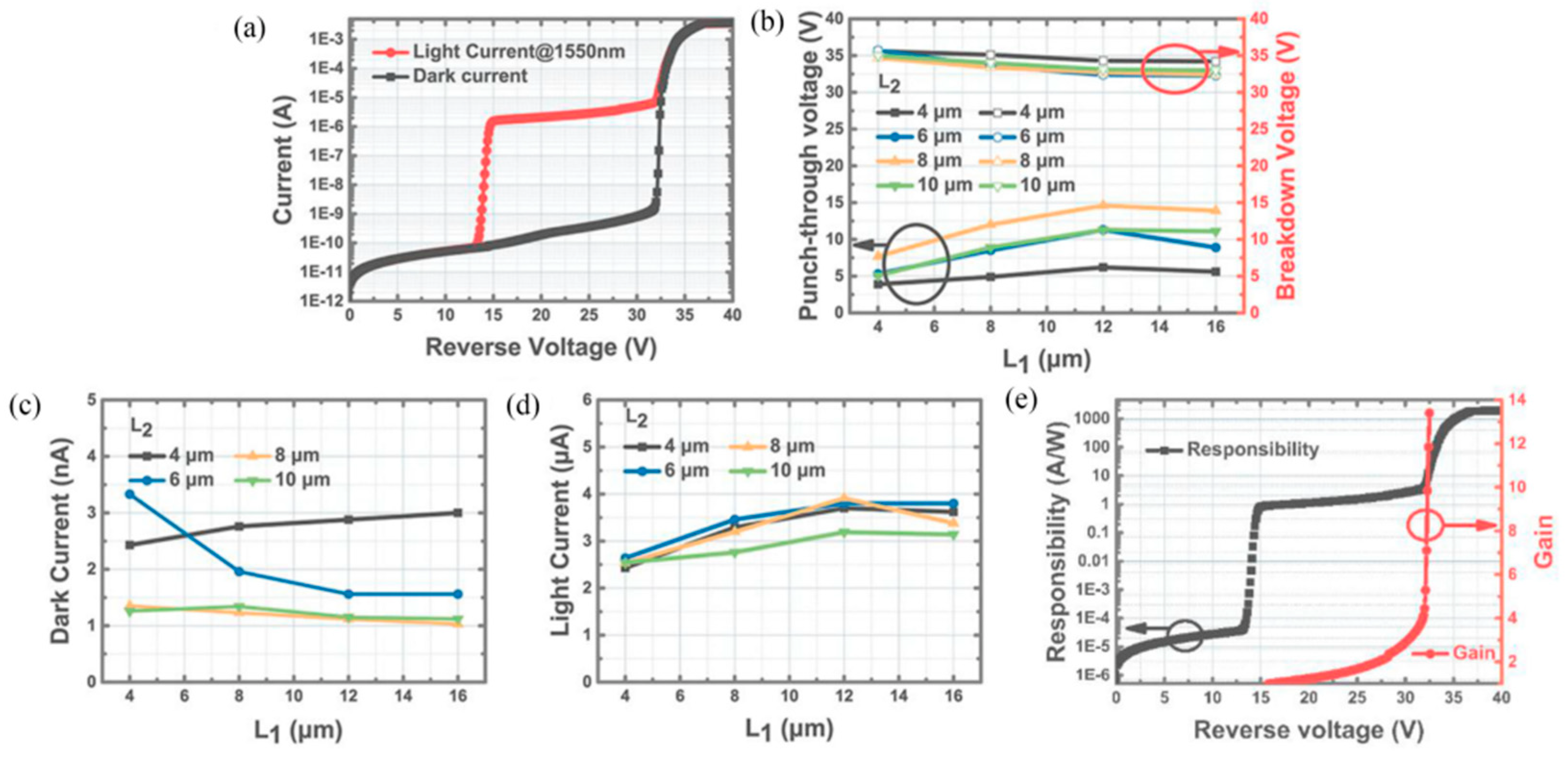


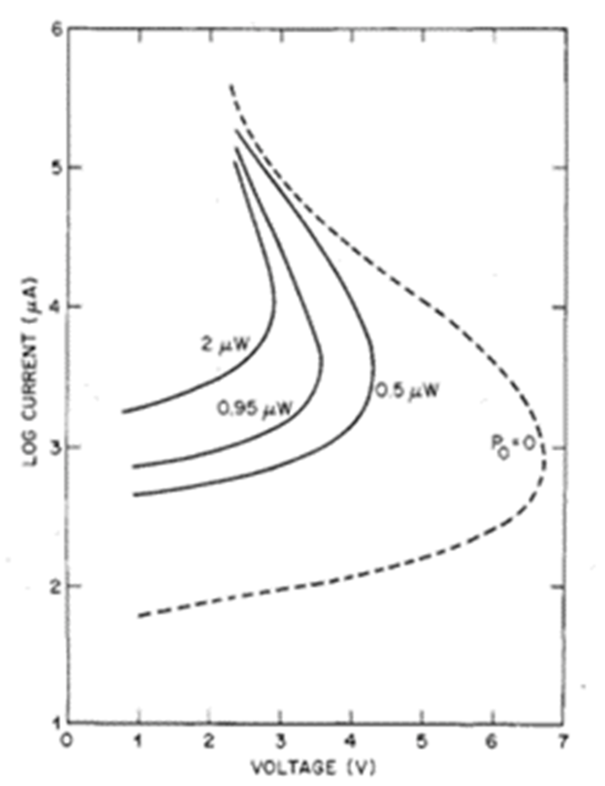
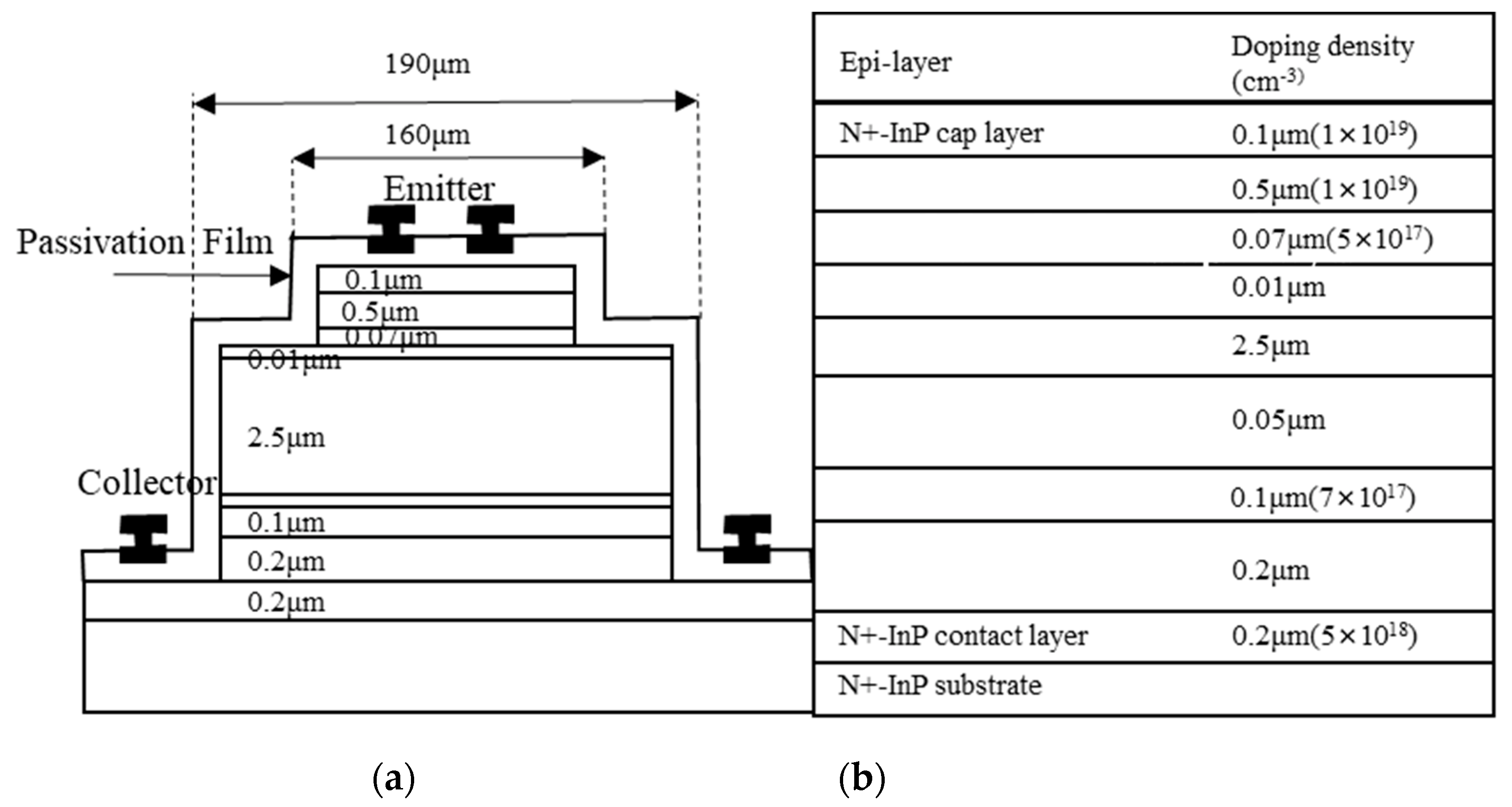
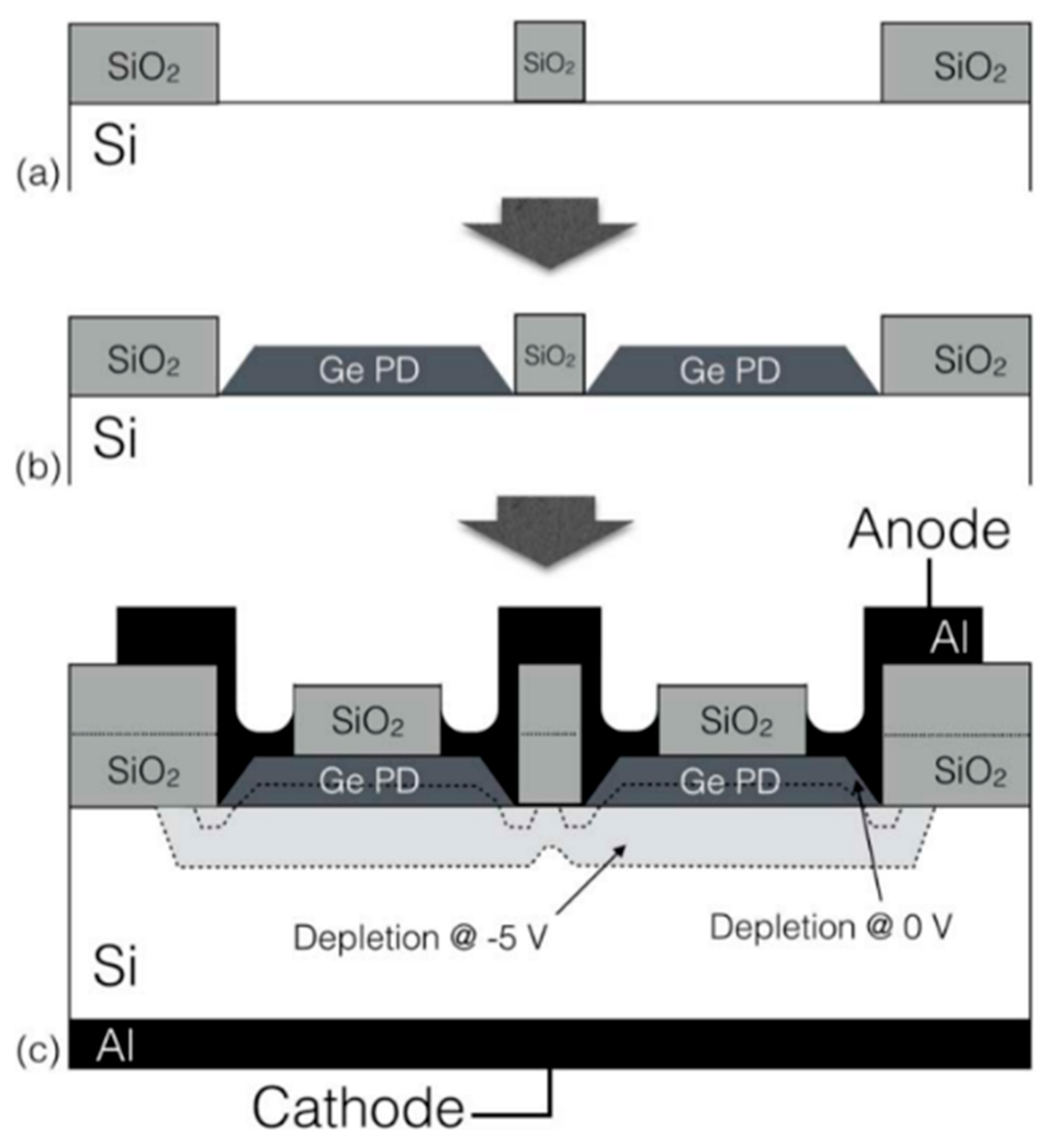
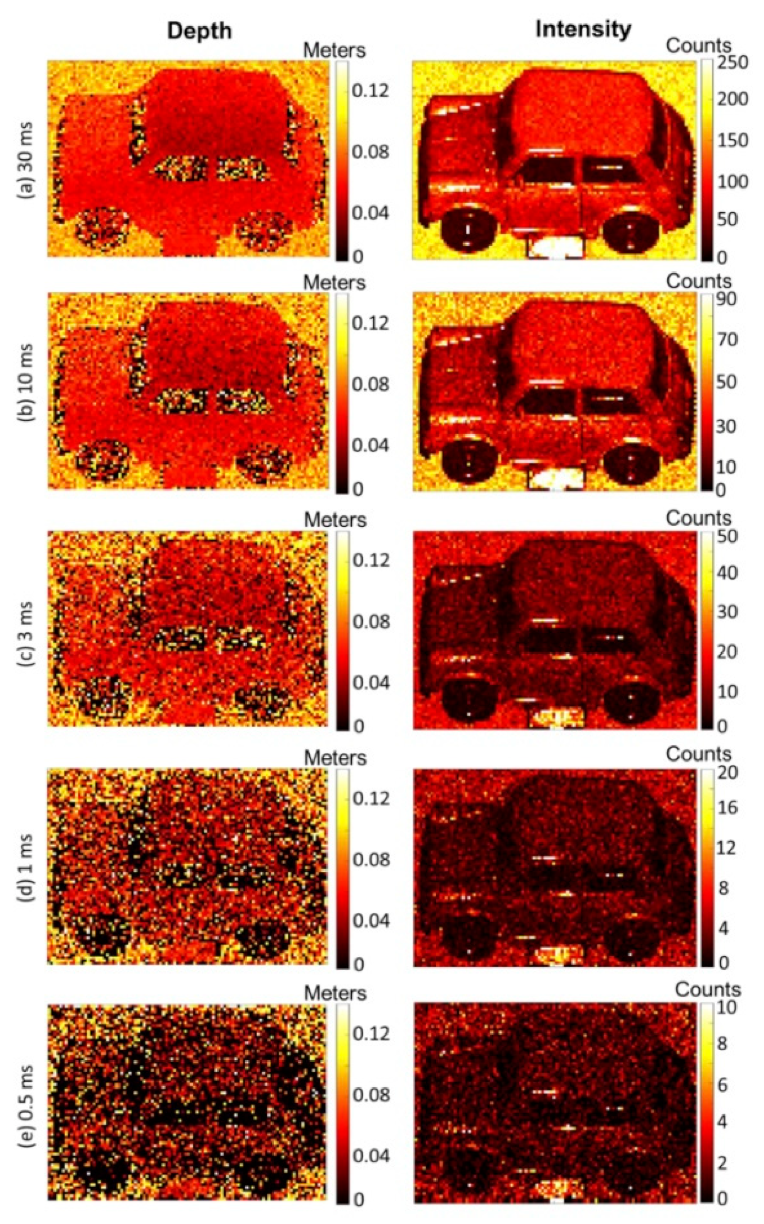
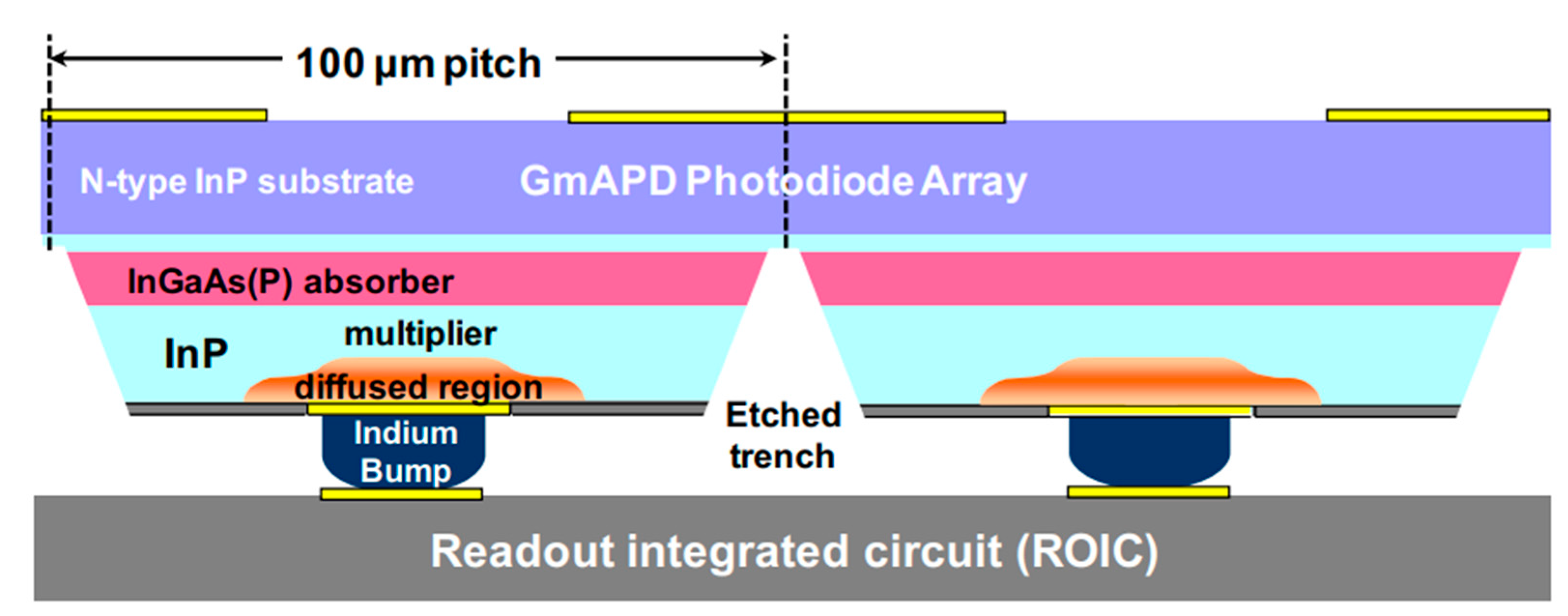

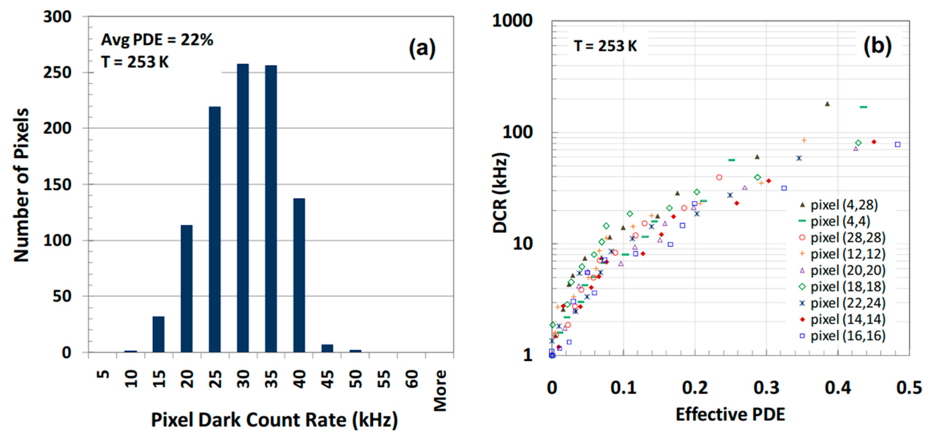
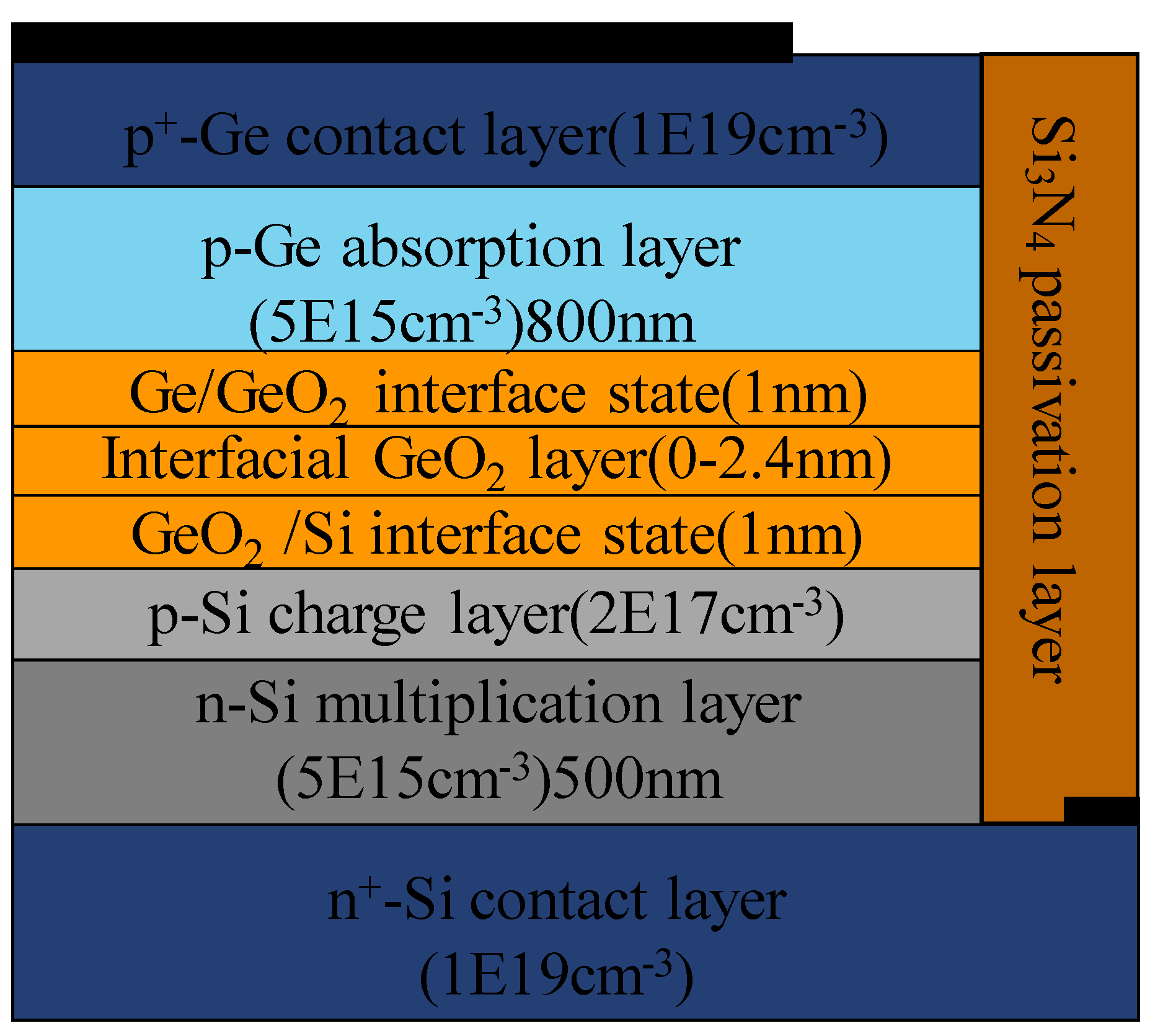

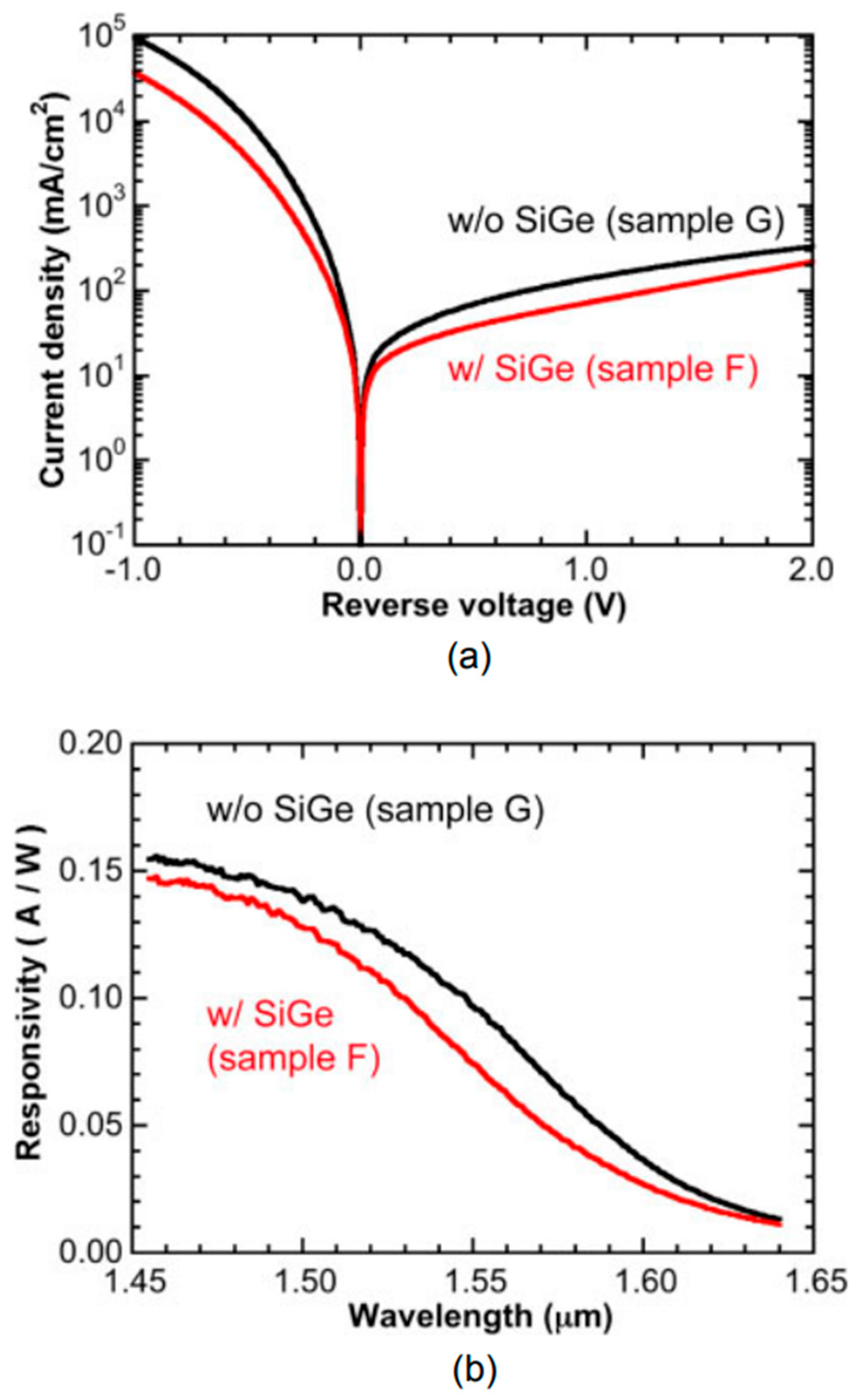
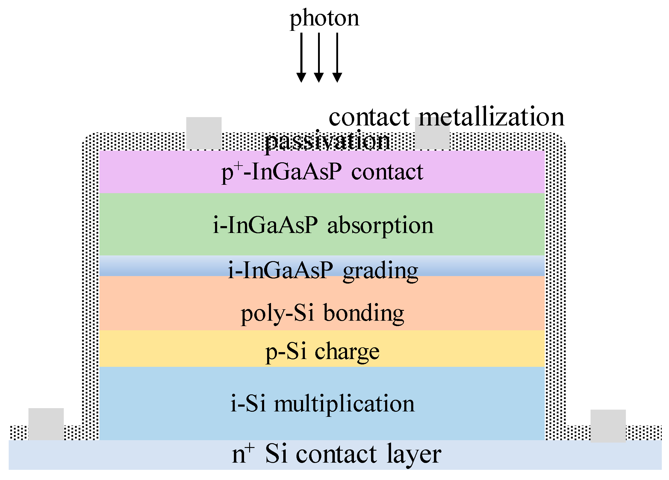
Disclaimer/Publisher’s Note: The statements, opinions and data contained in all publications are solely those of the individual author(s) and contributor(s) and not of MDPI and/or the editor(s). MDPI and/or the editor(s) disclaim responsibility for any injury to people or property resulting from any ideas, methods, instructions or products referred to in the content. |
© 2023 by the authors. Licensee MDPI, Basel, Switzerland. This article is an open access article distributed under the terms and conditions of the Creative Commons Attribution (CC BY) license (https://creativecommons.org/licenses/by/4.0/).