


Directional Scattering Switching from an All-Dielectric Phase Change Metasurface


Abstract
1. Introduction
2. Methods
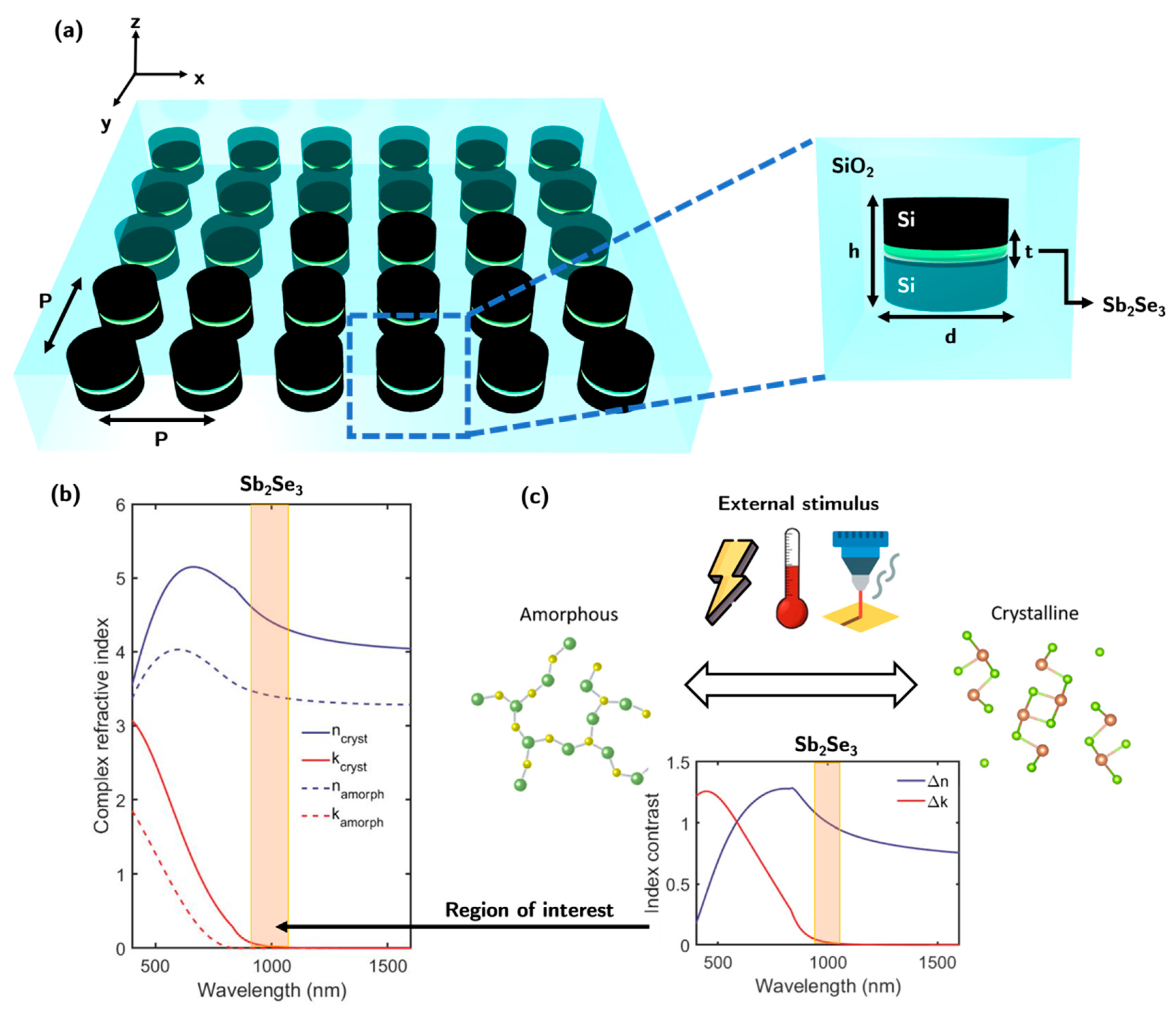
3. Device Design
4. Results and Discussion
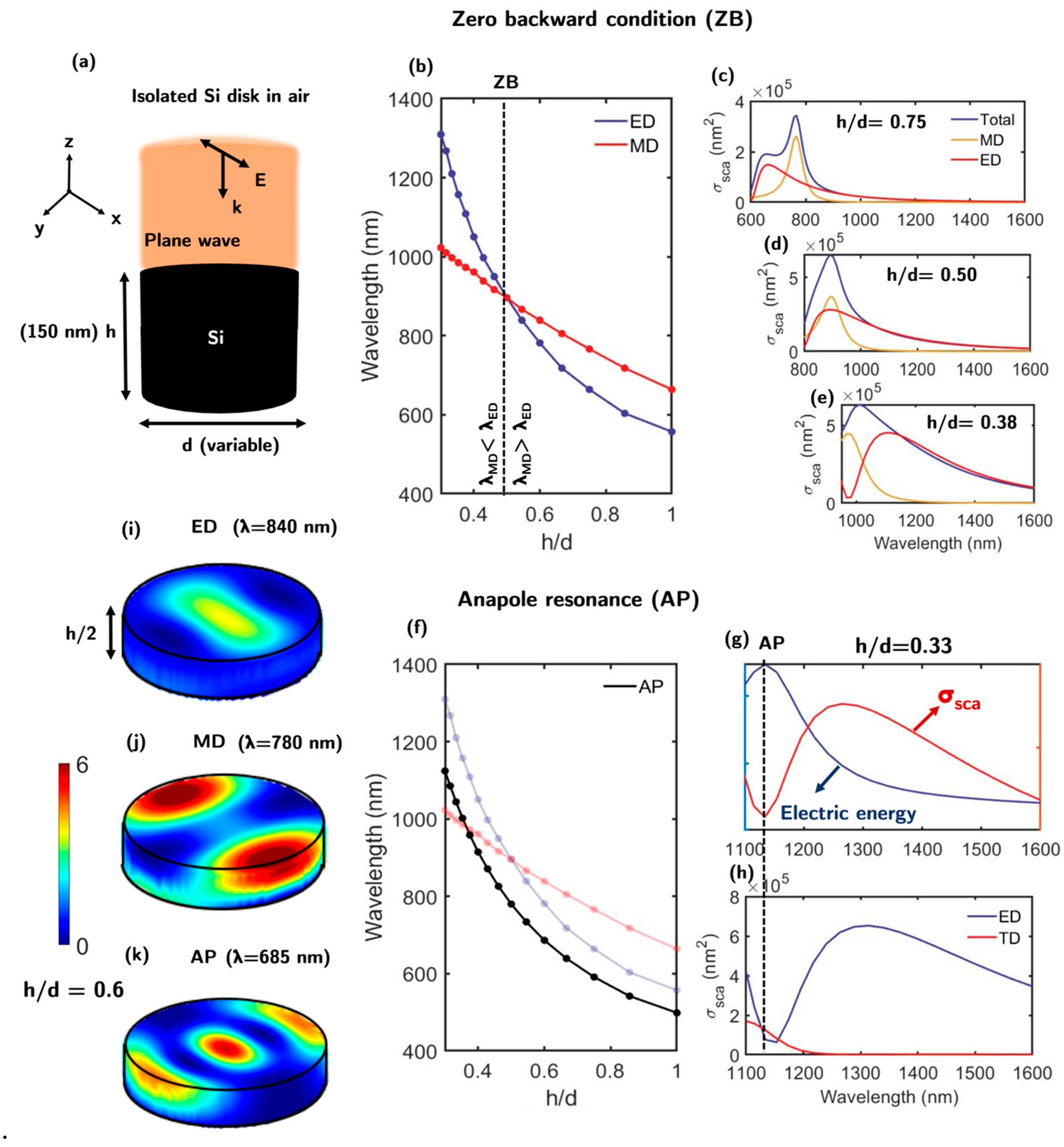
4.1. The Building Blocks
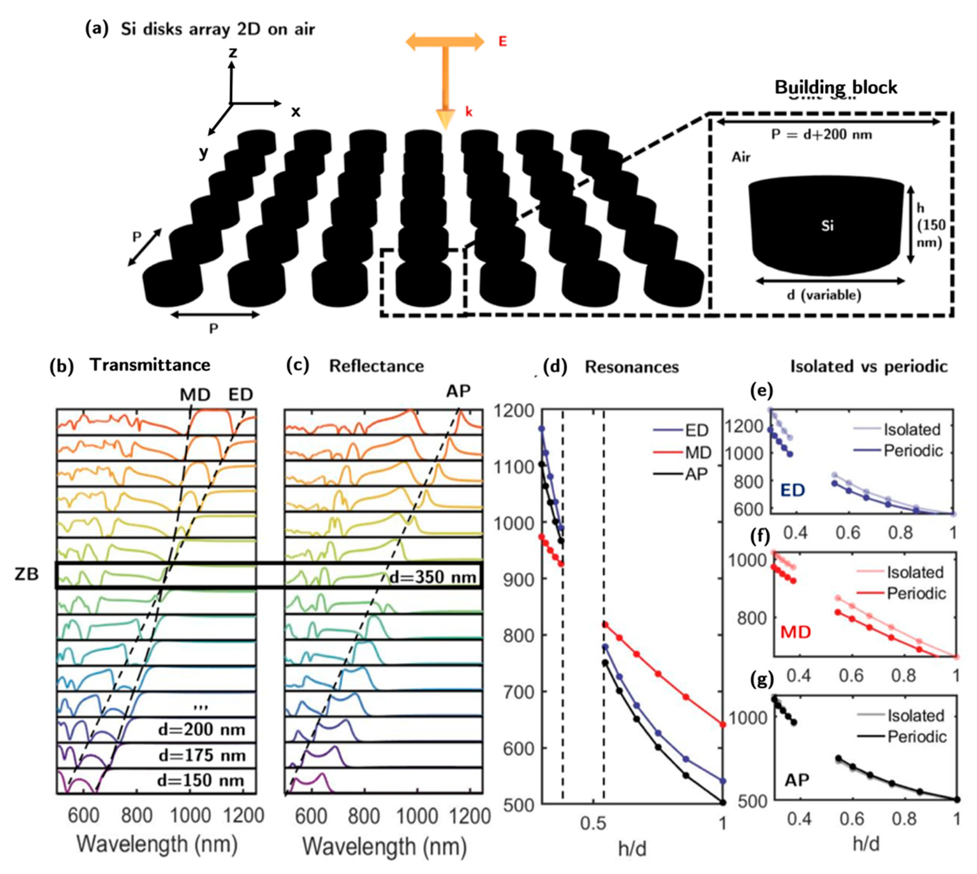
4.2. The Metasurface in Air
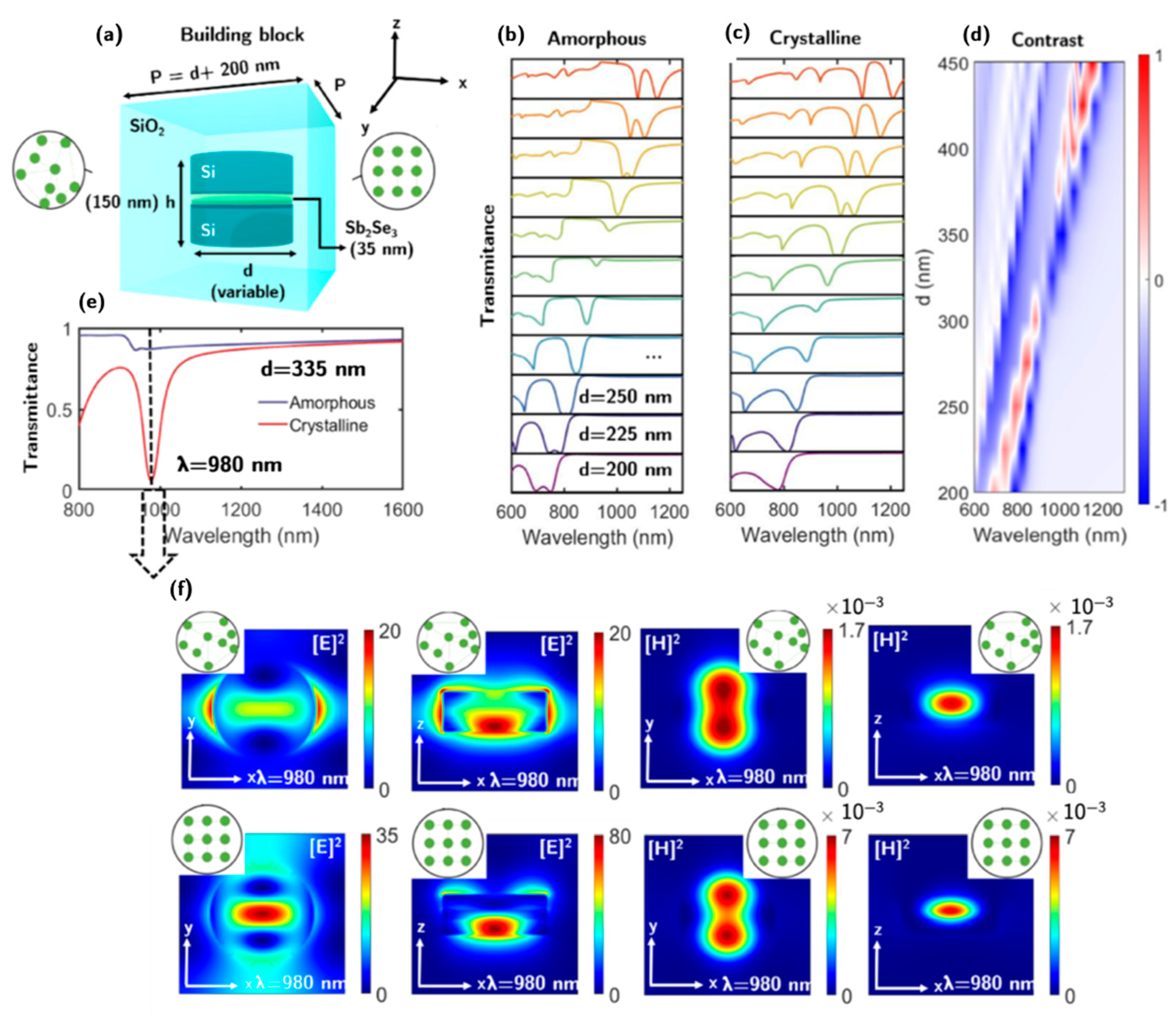
4.3. The Reconfigurable Metasurface in SiO2
5. Conclusions
Supplementary Materials
Author Contributions
Funding
Data Availability Statement
Conflicts of Interest
References
- Liu, J.; He, H.; Xiao, D.; Yin, S.; Ji, W.; Jiang, S.; Luo, D.; Wang, B.; Liu, Y. Recent Advances of Plasmonic Nanoparticles and Their Applications. Materials 2018, 11, 1833. [Google Scholar] [CrossRef] [PubMed]
- Tang, H.; Chen, C.J.; Huang, Z.; Bright, J.; Meng, G.; Liu, R.S.; Wu, N. Plasmonic Hot Electrons for Sensing, Photodetection, and Solar Energy Applications: A Perspective. J. Chem. Phys. 2020, 152, 220901. [Google Scholar] [CrossRef]
- Wang, L.; Hasanzadeh Kafshgari, M.; Meunier, M. Optical Properties and Applications of Plasmonic-Metal Nanoparticles. Adv. Funct. Mater. 2020, 30, 1–28. [Google Scholar] [CrossRef]
- Doiron, B.; Mota, M.; Wells, M.P.; Bower, R.; Mihai, A.; Li, Y.; Cohen, L.F.; Alford, N.M.N.; Petrov, P.K.; Oulton, R.F.; et al. Quantifying Figures of Merit for Localized Surface Plasmon Resonance Applications: A Materials Survey. ACS Photonics 2019, 6, 240–259. [Google Scholar] [CrossRef]
- Hutter, E.; Fendler, J.H. Exploitation of Localized Surface Plasmon Resonance. Adv. Mater. 2004, 16, 1685–1706. [Google Scholar] [CrossRef]
- Bohren, C.F. Absorption and Scattering of Light by Small Particles. Phys. Bull. 1983, 35, 104. [Google Scholar] [CrossRef]
- Jauffred, L.; Samadi, A.; Klingberg, H.; Bendix, P.M.; Oddershede, L.B. Plasmonic Heating of Nanostructures. Chem. Rev. 2019, 119, 8087–8130. [Google Scholar] [CrossRef]
- Nieto-Vesperinas, M. Fundamentals of Mie Scattering; Elsevier Ltd.: Amsterdam, The Netherlands, 2019; ISBN 9780081024034. [Google Scholar]
- Zambrana-Puyalto, X.; D’Ambrosio, D.; Gagliardi, G. Excitation Mechanisms of Whispering Gallery Modes with Direct Light Scattering. Laser Photonics Rev. 2021, 15, 1–10. [Google Scholar] [CrossRef]
- Foreman, M.R.; Vollmer, F. Theory of Resonance Shifts of Whispering Gallery Modes by Arbitrary Plasmonic Nanoparticles. New J. Phys. 2013, 15, 083006. [Google Scholar] [CrossRef]
- Chiasera, A.; Dumeige, Y.; Féron, P.; Ferrari, M.; Jestin, Y.; Conti, G.N.; Pelli, S.; Soria, S.; Righini, G.C. Spherical Whispering-Gallery-Mode Microresonators. Laser Photonics Rev. 2010, 4, 457–482. [Google Scholar] [CrossRef]
- Yang, S.; Wang, Y.; Sun, H.D. Advances and Prospects for Whispering Gallery Mode Microcavities. Adv. Opt. Mater. 2015, 3, 1136–1162. [Google Scholar] [CrossRef]
- Tribelsky, M.I.; Geffrin, J.M.; Litman, A.; Eyraud, C.; Moreno, F. Small Dielectric Spheres with High Refractive Index as New Multifunctional Elements for Optical Devices. Sci. Rep. 2015, 5, 1–7. [Google Scholar] [CrossRef] [PubMed]
- Kerker, M.; Wang, D.S.; Giles, C.L. Electromagnetic Scattering by Magnetic Spheres. J. Opt. Soc. Am. 1983, 73, 765–767. [Google Scholar] [CrossRef]
- García-Etxarri, A.; Gómez-Medina, R.; Froufe-Pérez, L.S.; López, C.; Chantada, L.; Scheffold, F.; Aizpurua, J.; Nieto-Vesperinas, M.; Sáenz, J.J. Strong Magnetic Response of Submicron Silicon Particles in the Infrared. Opt. Express 2011, 19, 4815. [Google Scholar] [CrossRef]
- Geffrin, J.M.; García-Cámara, B.; Gómez-Medina, R.; Albella, P.; Froufe-Pérez, L.S.; Eyraud, C.; Litman, A.; Vaillon, R.; González, F.; Nieto-Vesperinas, M.; et al. Magnetic and Electric Coherence in Forward-and Back-Scattered Electromagnetic Waves by a Single Dielectric Subwavelength Sphere. Nat. Commun. 2012, 3, 1171. [Google Scholar] [CrossRef]
- Tribelsky, M.I.; Geffrin, J.M.; Litman, A.; Eyraud, C.; Moreno, F. Directional Fano Resonances in Light Scattering by a High Refractive Index Dielectric Sphere. Phys. Rev. B 2016, 94, 1–5. [Google Scholar] [CrossRef]
- Sugimoto, H.; Fujii, M. Colloidal Mie Resonators for All-Dielectric Metaoptics. Adv. Photonics Res. 2021, 2, 2000111. [Google Scholar] [CrossRef]
- Evlyukhin, A.B.; Reinhardt, C.; Chichkov, B.N. Multipole Light Scattering by Nonspherical Nanoparticles in the Discrete Dipole Approximation. Phys. Rev. B Condens. Matter Mater. Phys. 2011, 84, 1–8. [Google Scholar] [CrossRef]
- Person, S.; Jain, M.; Lapin, Z.; Sáenz, J.J.; Wicks, G.; Novotny, L. Demonstration of Zero Optical Backscattering from Single Nanoparticles. Nano Lett. 2013, 13, 1806–1809. [Google Scholar] [CrossRef]
- Lee, D.; Kim, M.; Kim, J.; Hong, H.; Badloe, T.; Sung Kim, D.; Rho, J. All-Dielectric Metasurface Imaging Platform Applicable to Laser Scanning Microscopy with Enhanced Axial Resolution and Wavelength Selection. Opt. Mater. Express 2019, 9, 3248. [Google Scholar] [CrossRef]
- Reineke, B.; Sain, B.; Zhao, R.; Carletti, L.; Liu, B.; Huang, L.; De Angelis, C.; Zentgraf, T. Silicon Metasurfaces for Third Harmonic Geometric Phase Manipulation and Multiplexed Holography. Nano Lett. 2019, 19, 6585–6591. [Google Scholar] [CrossRef] [PubMed]
- Wu, C.; Arju, N.; Kelp, G.; Fan, J.A.; Dominguez, J.; Gonzales, E.; Tutuc, E.; Brener, I.; Shvets, G. Spectrally Selective Chiral Silicon Metasurfaces Based on Infrared Fano Resonances. Nat. Commun. 2014, 5, 1–9. [Google Scholar] [CrossRef] [PubMed]
- Holsteen, A.L.; Cihan, A.F.; Brongersma, M.L. Temporal Color Mixing and Dynamic Beam Shaping with Silicon Metasurfaces. Science 2019, 365, 257–260. [Google Scholar] [CrossRef] [PubMed]
- Zhou, Z.; Li, J.; Su, R.; Yao, B.; Fang, H.; Li, K.; Zhou, L.; Liu, J.; Stellinga, D.; Reardon, C.P.; et al. Efficient Silicon Metasurfaces for Visible Light. ACS Photonics 2017, 4, 544–551. [Google Scholar] [CrossRef]
- Duan, H.; Hu, Y.; Wang, X.; Luo, X.; Ou, X.; Li, L.; Chen, Y.; Yang, P.; Wang, S. All-Dielectric Metasurfaces for Polarization Manipulation: Principles and Emerging Applications. Nanophotonics 2020, 9, 3755–3780. [Google Scholar] [CrossRef]
- Danila, O.; Manaila-Maximean, D. Bifunctional Metamaterials Using Spatial Phase Gradient Architectures: Generalized Reflection and Refraction Considerations. Materials 2021, 14, 2201. [Google Scholar] [CrossRef]
- Danila, O. Polyvinylidene Fluoride-Based Metasurface for High-Quality Active Switching and Spectrum Shaping in the Terahertz g-Band. Polymers 2021, 13, 1860. [Google Scholar] [CrossRef]
- Staude, I.; Miroshnichenko, A.E.; Decker, M.; Fofang, N.T.; Liu, S.; Gonzales, E.; Dominguez, J.; Luk, T.S.; Neshev, D.N.; Brener, I.; et al. Tailoring Directional Scattering through Magnetic and Electric Resonances in Subwavelength Silicon Nanodisks. ACS Nano 2013, 7, 7824–7832. [Google Scholar] [CrossRef]
- Wang, Q.; Rogers, E.T.F.; Gholipour, B.; Wang, C.M.; Yuan, G.; Teng, J.; Zheludev, N.I. Optically Reconfigurable Metasurfaces and Photonic Devices Based on Phase Change Materials. Nat. Photonics 2016, 10, 60–65. [Google Scholar] [CrossRef]
- Chu, C.H.; Tseng, M.L.; Chen, J.; Wu, P.C.; Chen, Y.H.; Wang, H.C.; Chen, T.Y.; Hsieh, W.T.; Wu, H.J.; Sun, G.; et al. Active Dielectric Metasurface Based on Phase-Change Medium. Laser Photonics Rev. 2016, 10, 986–994. [Google Scholar] [CrossRef]
- Raeis-Hosseini, N.; Rho, J. Metasurfaces Based on Phase-Change Material as a Reconfigurable Platform for Multifunctional Devices. Materials 2017, 10, 1046. [Google Scholar] [CrossRef] [PubMed]
- Ruiz de Galarreta, C.; Carrillo, S.G.C.; Au, Y.Y.; Gemo, E.; Trimby, L.; Shields, J.; Humphreys, E.; Faneca, J.; Cai, L.; Baldycheva, A.; et al. Tunable Optical Metasurfaces Enabled by Chalcogenide Phase-Change Materials: From the Visible to the THz. J. Opt. 2020, 22, 114001. [Google Scholar] [CrossRef]
- Zhang, Y.; Fowler, C.; Liang, J.; Azhar, B.; Shalaginov, M.Y.; Deckoff-Jones, S.; An, S.; Chou, J.B.; Roberts, C.M.; Liberman, V.; et al. Electrically Reconfigurable Non-Volatile Metasurface Using Low-Loss Optical Phase-Change Material. Nat. Nanotechnol. 2021, 16, 661–666. [Google Scholar] [CrossRef] [PubMed]
- Xiao, S.; Wang, T.; Liu, T.; Zhou, C.; Jiang, X.; Zhang, J. Active Metamaterials and Metadevices: A Review. J. Phys. D. Appl. Phys. 2020, 53, 503002. [Google Scholar] [CrossRef]
- Liu, T.; Han, Z.; Duan, J.; Xiao, S. Phase-Change Metasurfaces for Dynamic Image Display and Information Encryption. Phys. Rev. Appl. 2022, 18, 1. [Google Scholar] [CrossRef]
- Wuttig, M.; Bhaskaran, H.; Taubner, T. Phase-Change Materials for Non-Volatile Photonic Applications. Nat. Photonics 2017, 11, 465–476. [Google Scholar] [CrossRef]
- Wuttig, M.; Yamada, N. Phase-Change Materials for Rewriteable Data Storage. Nat. Mater. 2007, 6, 824–832. [Google Scholar] [CrossRef]
- Dong, W.; Liu, H.; Behera, J.K.; Lu, L.; Ng, R.J.H.; Sreekanth, K.V.; Zhou, X.; Yang, J.K.W.; Simpson, R.E. Wide Bandgap Phase Change Material Tuned Visible Photonics. Adv. Funct. Mater. 2019, 29, 1806181. [Google Scholar] [CrossRef]
- Delaney, M.; Zeimpekis, I.; Du, H.; Yan, X.; Banakar, M.; Thomson, D.J.; Hewak, D.W.; Muskens, O.L. Nonvolatile Programmable Silicon Photonics Using an Ultralow-Loss Sb 2 Se 3 Phase Change Material. Sci. Adv. 2021, 7, 1–8. [Google Scholar] [CrossRef]
- Lu, L.; Reniers, S.F.G.; Wang, Y.; Jiao, Y.; Simpson, R.E. Reconfigurable InP Waveguide Components Using the Sb2S3phase Change Material. J. Opt. 2022, 24, 094001. [Google Scholar] [CrossRef]
- Ruiz De Galarreta, C.; Sinev, I.; Arseny, A.M.; Trofimov, P.; Ladutenko, K.; Garcia-Cuevas Carrillo, S.; Gemo, E.; Baldycheva, A.; Bertolotti, J.; Wright, C.D. Reconfigurable Multilevel Control of Hybrid. Optica 2020, 7, 476–484. [Google Scholar] [CrossRef]
- Hinamoto, T.; Fujii, M. MENP: An Open-Source MATLAB Implementation of Multipole Expansion for Nanophotonics. OSA Contin. 2021, 4, 1640. [Google Scholar] [CrossRef]
- Braid, G.; Ruiz de Galarreta, C.; Comley, A.; Bertolotti, J.; Wright, C.D. Optical and Thermal Design and Analysis of Phase-Change Metalenses for Active Numerical Aperture Control. Nanomaterials 2022, 12, 2689. [Google Scholar] [CrossRef] [PubMed]
- Delaney, M.; Zeimpekis, I.; Lawson, D.; Hewak, D.W.; Muskens, O.L. A New Family of Ultralow Loss Reversible Phase-Change Materials for Photonic Integrated Circuits: Sb 2 S 3 and Sb 2 Se 3. Adv. Funct. Mater. 2020, 30, 2002447. [Google Scholar] [CrossRef]
- Shongalova, A.; Correia, M.R.; Teixeira, J.P.; Leitão, J.P.; González, J.C.; Ranjbar, S.; Garud, S.; Vermang, B.; Cunha, J.M.V.; Salomé, P.M.P.; et al. Growth of Sb2Se3 Thin Films by Selenization of RF Sputtered Binary Precursors. Sol. Energy Mater. Sol. Cells 2018, 187, 219–226. [Google Scholar] [CrossRef]
- Palik, E.D. Handbook of Optical Constants of Solids; Academic Press: Cambridge, UK, 1998. [Google Scholar]
- De Galarreta, C.R.; Sinev, I.; Alexeev, A.M.; Trofimov, P.; Ladutenko, K.; Carrillo, S.G.-C.; Gemo, E.; Baldycheva, A.; Nagareddy, V.K.; Bertolotti, J.; et al. All-Dielectric Silicon/Phase-Change Optical Metasurfaces with Independent and Reconfigurable Control of Resonant Modes. arXiv 2019, 1–34. [Google Scholar] [CrossRef]
- González-Colsa, J.; Olarte-Plata, J.D.; Bresme, F.; Albella, P. Enhanced Thermo-Optical Response by Means of Anapole Excitation. J. Phys. Chem. Lett. 2022, 13, 6230–6235. [Google Scholar] [CrossRef]
- Lukyanchuk, B.; Paniagua-Domínguez, R.; Kuznetsov, A.I.; Miroshnichenko, A.E.; Kivshar, Y.S. Suppression of Scattering for Small Dielectric Particles: Anapole Mode and Invisibility. Philos. Trans. R. Soc. A Math. Phys. Eng. Sci. 2017, 375, 20160069. [Google Scholar] [CrossRef]
- Miroshnichenko, A.E.; Evlyukhin, A.B.; Yu, Y.F.; Bakker, R.M.; Chipouline, A.; Kuznetsov, A.I.; Luk’yanchuk, B.; Chichkov, B.N.; Kivshar, Y.S. Nonradiating Anapole Modes in Dielectric Nanoparticles. Nat. Commun. 2015, 6, 1–8. [Google Scholar] [CrossRef]
- Savinov, V.; Papasimakis, N.; Tsai, D.P.; Zheludev, N.I. Optical Anapoles. Commun. Phys. 2019, 2, 10–13. [Google Scholar] [CrossRef]
- Liu, W.; Shi, J.; Lei, B.; Hu, H.; Miroshnichenko, A.E. Efficient Excitation and Tuning of Toroidal Dipoles within Individual Homogenous Nanoparticles. Opt. Express 2015, 23, 24738. [Google Scholar] [CrossRef] [PubMed]
- Baryshnikova, K.V.; Smirnova, D.A.; Luk’yanchuk, B.S.; Kivshar, Y.S. Optical Anapoles: Concepts and Applications. Adv. Opt. Mater. 2019, 7, 1–13. [Google Scholar] [CrossRef]
- Zenin, V.A.; Evlyukhin, A.B.; Novikov, S.M.; Yang, Y.; Malureanu, R.; Lavrinenko, A.V.; Chichkov, B.N.; Bozhevolnyi, S.I. Direct Amplitude-Phase Near-Field Observation of Higher-Order Anapole States. Nano Lett. 2017, 17, 7152–7159. [Google Scholar] [CrossRef] [PubMed]
- Díaz-Escobar, E.; Bauer, T.; Pinilla-Cienfuegos, E.; Barreda, Á.I.; Griol, A.; Kuipers, L.; Martínez, A. Radiationless Anapole States in On-Chip Photonics. Light Sci. Appl. 2021, 10, 204. [Google Scholar] [CrossRef] [PubMed]
- Sun, M.; Xu, X.; Sun, X.W.; Liang, X.; Valuckas, V.; Zheng, Y.; Paniagua-Domínguez, R.; Kuznetsov, A.I. Efficient Visible Light Modulation Based on Electrically Tunable All Dielectric Metasurfaces Embedded in Thin-Layer Nematic Liquid Crystals. Sci. Rep. 2019, 9, 8673. [Google Scholar] [CrossRef] [PubMed]
- Zhang, C.; Jing, J.; Wu, Y.; Fan, Y.; Yang, W.; Wang, S.; Song, Q.; Xiao, S. Stretchable All-Dielectric Metasurfaces with Polarization-Insensitive and Full-Spectrum Response. ACS Nano 2020, 14, 1418–1426. [Google Scholar] [CrossRef] [PubMed]
- Yang, Y.; Kravchenko, I.I.; Briggs, D.P.; Valentine, J. All-Dielectric Metasurface Analogue of Electromagnetically Induced Transparency. Nat. Commun. 2014, 5, 5753. [Google Scholar] [CrossRef] [PubMed]


Disclaimer/Publisher’s Note: The statements, opinions and data contained in all publications are solely those of the individual author(s) and contributor(s) and not of MDPI and/or the editor(s). MDPI and/or the editor(s) disclaim responsibility for any injury to people or property resulting from any ideas, methods, instructions or products referred to in the content. |
© 2023 by the authors. Licensee MDPI, Basel, Switzerland. This article is an open access article distributed under the terms and conditions of the Creative Commons Attribution (CC BY) license (https://creativecommons.org/licenses/by/4.0/).
Share and Cite
Santos, G.; Losurdo, M.; Moreno, F.; Gutiérrez, Y. Directional Scattering Switching from an All-Dielectric Phase Change Metasurface. Nanomaterials 2023, 13, 496. https://doi.org/10.3390/nano13030496
Santos G, Losurdo M, Moreno F, Gutiérrez Y. Directional Scattering Switching from an All-Dielectric Phase Change Metasurface. Nanomaterials. 2023; 13(3):496. https://doi.org/10.3390/nano13030496
Chicago/Turabian StyleSantos, Gonzalo, Maria Losurdo, Fernando Moreno, and Yael Gutiérrez. 2023. "Directional Scattering Switching from an All-Dielectric Phase Change Metasurface" Nanomaterials 13, no. 3: 496. https://doi.org/10.3390/nano13030496
APA StyleSantos, G., Losurdo, M., Moreno, F., & Gutiérrez, Y. (2023). Directional Scattering Switching from an All-Dielectric Phase Change Metasurface. Nanomaterials, 13(3), 496. https://doi.org/10.3390/nano13030496