Communication

Barrier Height, Ideality Factor and Role of Inhomogeneities at the AlGaN/GaN Interface in GaN Nanowire Wrap-Gate Transistor

1
Advanced Material Research Center, Kumoh National Institute of Technology, Gumi 39177, Republic of Korea
2
Department of Robotics and Intelligent Machine Engineering, College of Mechanical and IT Engineering, Yeungnam University, Gyeongsan 38541, Republic of Korea
3
Department of Materials Science and Engineering, Kumoh National Institute of Technology, Gumi 39177, Republic of Korea
4
Department of Green Semiconductor System, Daegu Campus, Korea Polytechnics, Daegu 41765, Republic of Korea
*
Authors to whom correspondence should be addressed.
These authors contribute to equally to this work.
Nanomaterials 2023, 13(24), 3159; https://doi.org/10.3390/nano13243159
Submission received: 28 November 2023 / Revised: 12 December 2023 / Accepted: 15 December 2023 / Published: 17 December 2023

Abstract

:
It is essential to understand the barrier height, ideality factor, and role of inhomogeneities at the metal/semiconductor interfaces in nanowires for the development of next generation nanoscale devices. Here, we investigate the drain current (Ids)–gate voltage (Vgs) characteristics of GaN nanowire wrap-gate transistors (WGTs) for various gate potentials in the wide temperature range of 130–310 K. An anomalous reduction in the experimental barrier height and rise in the ideality factor with reducing the temperature have been perceived. It is noteworthy that the variations in barrier height and ideality factor are attributed to the spatial barrier inhomogeneities at the AlGaN/GaN interface in the GaN nanowire WGTs by assuming a double Gaussian distribution of barrier heights at 310–190 K (distribution 1) and 190–130 K (distribution 2). The standard deviation for distribution 2 is lower than that of distribution 1, which suggests that distribution 2 reflects more homogeneity at the AlGaN/GaN interface in the transistor’s source/drain regions than distribution 1.

1. Introduction

Nano-based field-effect transistors (FET) are involved with replacing existing conventional technology and have surged to be one of the potential solutions towards continuous complementary metal-oxide-semiconductor (CMOS) scaling. The semiconductor-based nanowires have been significantly explored because of their most promising applications for next-generation high-quality optoelectronic/electronic devices [1,2,3]. The scaling of numerous transistor types is based on geometries as in Fin-FET, omega gate, tri-gate, and wrap-gate (WG) or gate-all-around (GAA) devices [4,5,6,7,8,9,10,11]. WG-based devices contribute particularly remarkable performance advantages over other geometries because of their extreme electrostatic controls. During recent years, WG-based devices fabricated by bottom-up techniques have been intensively studied as the fundamental building block for nano-electronic devices and circuit technologies. The top-down fabrication of nanowire WG transistors (WGTs) based on a sacrificial layer has many advantages in contrast to a bottom-up approach: reduced device size, large-scale feasibility with high yield, and an orderly alignment of parallel nanowires. It has already been reported that GaN-based nanowires have made significant progress. GaN-based devices have attractive features for great device performance such as high-speed, high-power, high-frequency, and high-temperature operations. A GaN nanowire-based device can control its normally off state with a high Ion/Ioff ratio, a low gate leakage current, and a high conductance. For this paper, we fabricated a device using the top-down process and investigated the electrical transport properties in a GaN nanowire WGT on a GaN-on-insulator (GaNOI) substrate.
Knowledge of nanowire device operation at cryogenic temperatures is of special interest because, at room temperature, nanowire devices do not yield broad information about their carrier transport characteristics. The current–voltage (I–V) properties of nanowires as a function of temperature allows the identification of various current flow mechanisms and additional significant electrical transport across the metal/semiconductor interface (i.e., source/drain regions) [12,13]. A good understanding of barrier heights, ideality factor, and the role of inhomogeneities at the metal/semiconductor interface in nanowires led to the concept of the thermionic emission (TE) mechanism by assuming the coexistence of a double Gaussian distribution.
The metal/semiconductor interface is characterized by a certain work function. The fact it is Ohmic or Schottky depends on the boundary conditions at the interface which depends on a few variables, including the semiconductor doping concertation near the interface. High doping allows the tuning of the carriers across the barriers, reducing the contact resistance. Usually, after the preparation of Ohmic contacts for the fabrication of FETs in their source and drain regions, certain semiconductor contacts appear to have Ohmic behavior, but in truth, they are Schottky in nature. In experiments, a FET with two identical source and drain regions can be seen to have back-to-back Schottky contacts.
Here, we have studied the electrical transport mechanism in the GaN nanowire WGT as a function of temperature with variable gate bias. The temperature dependence of the barrier height (Φb0) and the ideality factor (η) values are found at the interface of AlGaN/GaN in the source/drain regions of the GaN nanowire WGT. Finally, we showed that the two linear regions in the variation of Φb0 versus 1/2 kT could be explained with the help of a double Gaussian distribution.

2. Materials and Methods
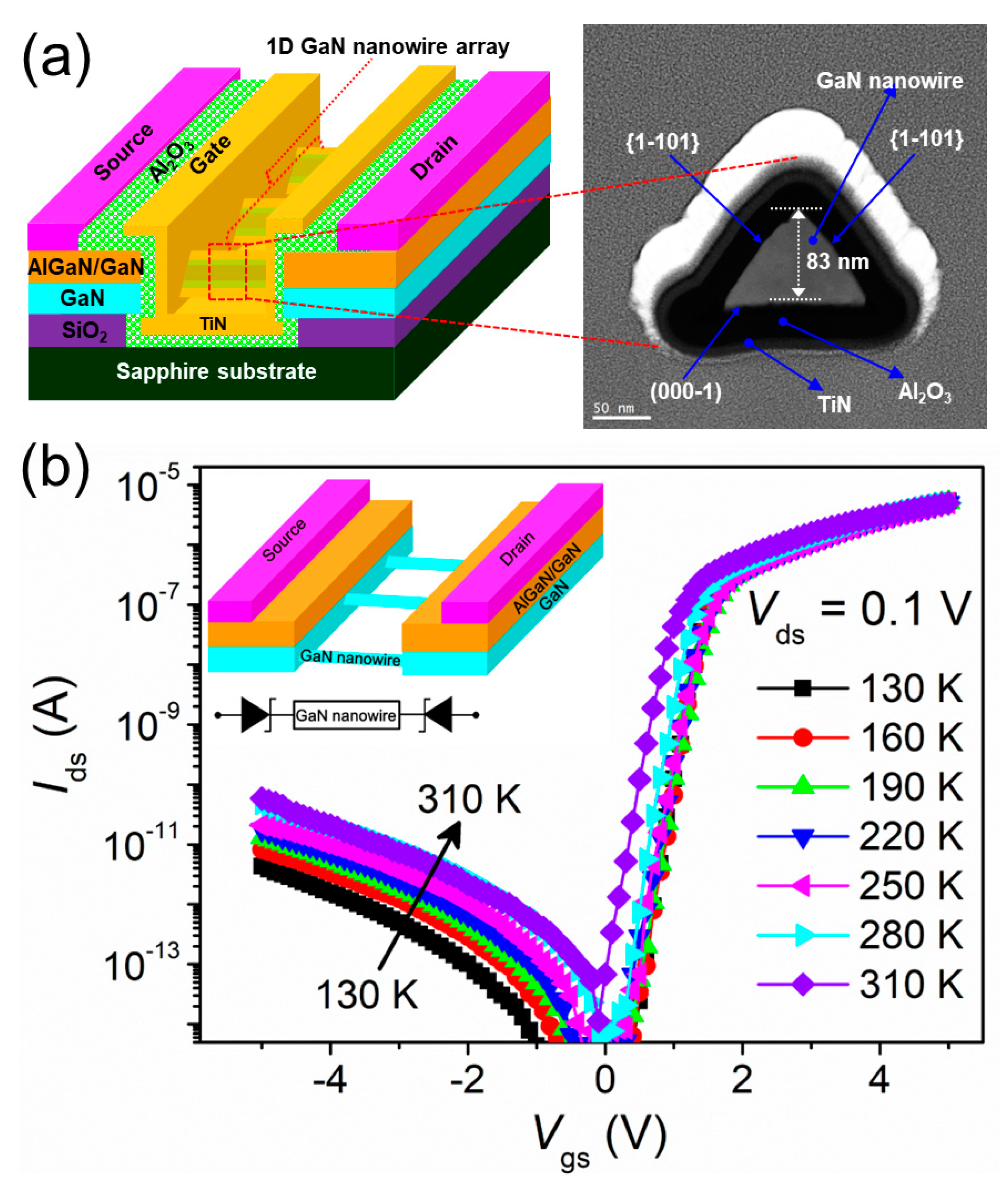
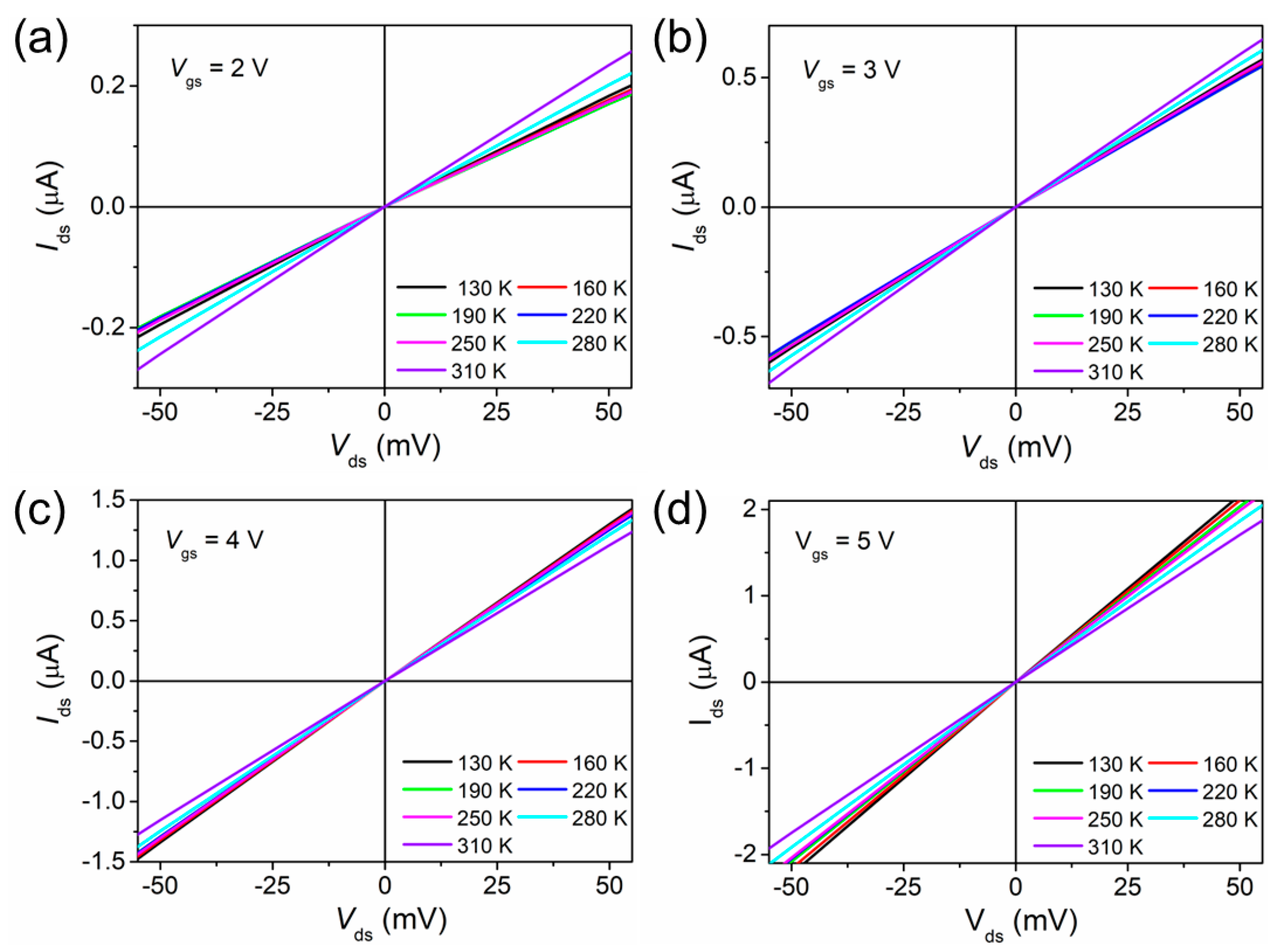
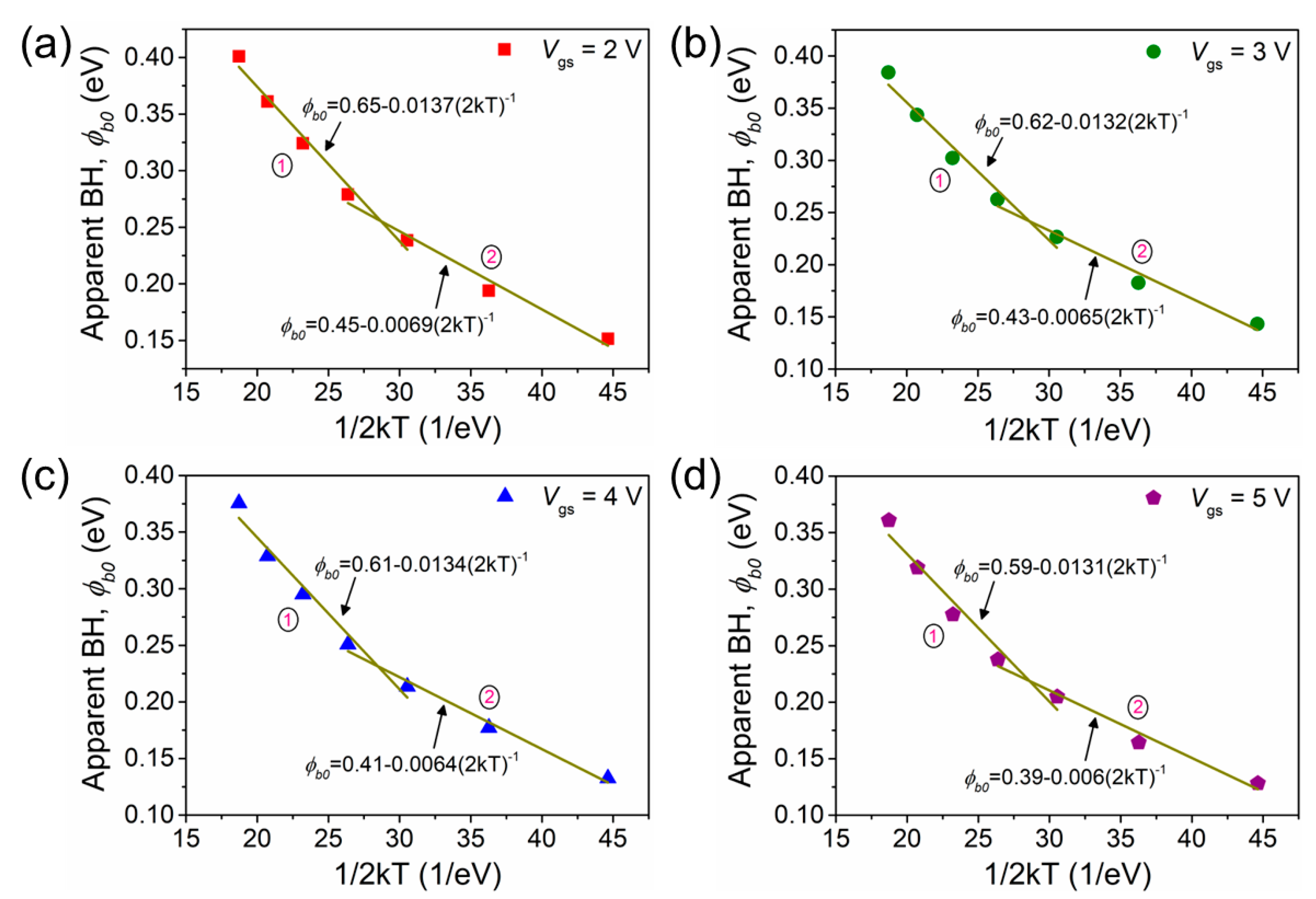
For the GaN nanowire WGT architecture, we used a GaNOI substrate based on Smart CutTM technology from the SOITEC Company by the dual-wafer transfer method [7]. A 4-inch diameter GaNOI substrate consists of 150 nm thick GaN film and 800 nm thick silicon-dioxide (SiO2) on a 0.65 mm thick sapphire wafer. Initially, the ‹11-20› phase was aligned by electron beam (e-beam) lithography on the GaNOI substrate with the help of poly(methyl methacrylate) (PMMA) resist. Using an inductively coupled plasma (ICP) dry etching process, the GaN film was selectively etched, and after this, the aligned film was dipped in 5% of tetramethylammonium hydroxide (i.e., TMAH was purchased from Transene company, Inc., Danvers, MA, USA) etchant solution at 90 °C for 10 min. The TMAH etchant solution entirely etches in the sideways direction instead of perpendicular c-plane (0001) direction. This etchant solution reduced the GaN film width along the ‹11-00› phase, giving 83 nm heights with similar triangular-shaped sidewall ‹11-01› phases. Next, the film was treated with a buffer-oxide etchant (BOE) solution to effectively remove the SiO2 layer under the structure of the GaN nanowires.
Next, selectively re-grow 50 nm and 20 nm thicknesses of undoped GaN and AlGaN films on the aligned GaN surface using a sophisticated metal-organic chemical vapor deposition (MOCVD) instrument. Here, a self-limiting re-growth in the ‹11-01› phase acted as an r-plane on the aligned GaN film. At this viewpoint, the surface of the r-plane consisted of nitrogen (N) atoms that were easily impelled by hydrogen (H) atoms in the MOCVD instrument and produced N-H bonds that limited growth and added stability in the plane direction. Hence, AlGaN/GaN films were not re-grown on the GaN nanowire but easily re-grown only on the source and drain regions. As a result of this procedure, the GaN nanowire’s area has not changed. In fact, the significance of re-grown AlGaN/GaN films on the source and drain regions decreases the series resistance through two-dimensional electron gas (2DEG) at the junction.
For WGT device fabrication, 10 nm and 20 nm thicknesses of gate-metal (TiN) and high-k gate oxide (Al2O3) were coated using plasma-enhanced atomic layer deposition (PE-ALD) method. The thicknesses of the coated materials are confirmed by the number of PE-ALD cycles, a deposition rate (growth per cycle) of ~0.1 nm/cycle was determined by an ellipsometry. Here, 100 and 200 PE-ALD cycles are relatively equal to ~10 nm and ~20 nm thickness of TiN and Al2O3 layers. Accordingly, metal layers (Ti/Al//Ni/Au) were coated as source and drain regions with an e-beam technique and followed by rapid thermal process at 850 °C for 30 s in N2 atmosphere. Finally, gate metal (Ni/Au) was coated as an outer contact for device measurements. The re-grown AlGaN film mobility (μd, 1630 cm2/V·s) and concentration (NS, 9.75 × 1012 cm−2) were confirmed using Hall-effect examination (Nanometrics, HL5500PC, Kanata, ON, Canada). The device architecture was examined with a field-emission tunneling electron microscope (FE-TEM, 200 kV FE, JEM-2100F, Tokyo, Japan). The temperature-dependent IV characteristics of the device were measured with a Keithley source unit (SCS-4200, Cleveland, OH, USA) connected to vacuum chamber (MST-6VC) with a low-temperature regulate system. The sensitivity of the temperature control system is ±1 K.

3. Results

Figure 1a (on the left side) illustrates the schematic architecture of the studied GaN nanowire WGT device. It has a 2 μm gate length consisting of 64 triangular-shaped one-dimensional nanowires, each having two similar ‹1-101› crystal facets. On the right side of Figure 1a, an FE-TEM (i.e., dark field mode) image clearly shows a triangular-shaped GaN nanowire core surrounded by gate-oxide and gate-metal. Figure 1b shows the drain current (Ids) versus gate voltage (Vgs) curves of the AlGaN/GaN-based GaN nanowire WGT as a function of temperature ranging from 130 to 310 K in steps of 30 K at a drain voltage of Vds = 0.1 V. The drain leakage current (Ids) clearly increases with temperature from 1.12 × 10⁻¹³ (at 130 K) to 2.15 × 10⁻¹² A (at 310 K) at a Vgs of −2 V. The increase in drain leakage current may be due to the surface-related traps and temperature-assisted tunneling mechanisms [14,15]. The inset of Figure 1b shows a simplified diagram of the fabricated device with a back-to-back Schottky configuration composed of two (source/drain) contacts in series with GaN nanowires.
The current across the barrier mainly consists of three types of electron transport mechanisms: thermionic emission (TE), thermionic field emission (TFE), and field emission (FE). The dominant mode of carrier transport can be determined from the characteristics of the tunneling parameter E00; E00 « kT for TE, E00kT for TFE, and E00 » kT for FE. E00 is evaluated from the doping concentration (Nd) of the measured semiconductor as in [16]:
E 00 = q h k T N d m * ε S
where h is Planck’s constant, q is the charge, T is the absolute temperature, k is the Boltzmann constant, εS is the permittivity of the GaN (i.e., εS = 9.2ε0), m* is effective mass (m* = 0.3 m0 [17], where m0 is mass of electron), and the value of Nd in the present work is ~5 × 1016 cm−3. E00 is calculated to be about 8 meV from Equation (1), which is smaller than the value of kT at room temperature. This means that TE is the dominant carrier transport mechanism in the GaN nanowire at room temperature.
To investigate the effect of the GaN nanowire structure on the device characteristics at the AlGaN/GaN interface, we further analyzed the temperature dependence of effective barrier height (Φb0) and ideality factor (η) at the interface for different gate potentials. A GaN nanowire WGT with two similar metal contacts at the AlGaN/GaN (source and drain) regions can be regarded as back-to-back Schottky diodes. In this device architecture, most of the voltage drop happens in the reverse-biased side [18,19]. The Φb0 and η parameters are extracted by using the following relations [13]:
I = I 0 exp q V η k T 1 e x p q V η k T
where I 0 = A * T 2 A   e x p q Φ b 0 k T   ,   V is the gate bias, A is the contact area, and A* is the effective Richardson’s constant. The theoretical value of A* is ~35.8 Acm−2K−2 based on the effective mass of AlGaN [17] and is used for the calculation of Φb0. Equation (1) is modified as follows:
  l n I exp ( q V / k T ) exp ( q V / k T ) 1 = l n I 0 + q V η k T
where V is the voltage drop across the junction, V = VdsIR, and here, R is the series resistance. The values of I0 at different gate potentials were obtained from the I–V measurements (Figure 2a–d) in the plot of ln[I exp(qV/kT/(exp(qV/kT) 1)] versus V for the reverse bias at each temperature. The values of η and Φb0 are extracted from the slope and y intercept using Equation (3).
At temperature of 310 K, the values of Φb0 (Figure 3a) and η (Figure 3b) for different gate voltages were, respectively, found to be 0.41 eV and 1.22 at 2 V, 0.39 eV and 1.45 at 3 V, 0.37 eV and 1.54 at 4 V, and 0.36 and 1.65 at 5 V. These values confirm that TE is the dominant current conduction mechanism in GaN nanowire-based devices at room temperature. It is clearly shown that Φb0 (Figure 3a) increases and η (Figure 3b) decreases with increasing temperature at a range of gate voltages. At 130 K, the values of Φb0 and η for various voltages were, respectively, found to be 0.15 eV and 4.4 at 2 V, 0.14 eV and 4.6 at 3 V, 0.12 eV and 4.8 at 4 V, and 0.11 eV and 4.9 at 5 V. It is worthwhile to note that these values of η are much better than found in previous studies of GaN-based nanowires and nano-rods [20,21,22,23]. This may be due to the low semiconductor doping concentration or influence of surface states at the interface compared to previous studies. These η values are higher than unity, however, indicating that TE is not the entire conduction mechanism. This typical signature may be the result of tunneling, interface states, electrical dipole formation, or barrier inhomogeneities [24,25]. Tunneling current is significant in nanoscale devices compared to bulk devices because the device size is comparable to or less than the zero bias depletion width [Wd]. Wd can be expressed as follows [24,25]:
W d = 2 ε S Φ b 0 V n q 2 N d 1 2
where Vn = kTln(NC/Nd) is the position of the conduction band (EC) edge with respect to the Fermi level position (EF) in a GaN nanowire. NC is the density of states in the conduction band minimum as given by NC = 2(2πm*kT/h2)3/2. Its values were ~9 × 10¹⁷ and 3.1 × 1018 cm−3 [24] at 130 K and 300 K. From Equation (4), the value of Wd varies in the range of 25–90 nm for all temperature barrier heights. These varied Wd values are comparable to a GaN nanowire height of ~83 nm, and hence, the tunneling current could be a major factor at the metal/AlGaN/GaN interface in GaN nanowires for all temperatures that drive the ideality factor above the unit value.
To further understand the nature of carrier transport in a GaN nanowire, we view an inhomogeneous metal contact at the AlGaN/GaN interface as a distribution of local high and low barrier height patches with nanoscale geometry. Here, electrical transport at low temperatures is dominated by low barrier height patches with a higher ideality factor as the carrier passes through the patches. At high temperatures, the carrier flows through high barrier patches causing the barrier height to increase and the ideality factor to decrease. Consequently, the barrier height at the AlGaN/GaN interface of the source/drain region is not constant but follows a Gaussian distribution due to the barrier inhomogeneities as in [26]:
P Φ b 0 = 1 σ S 2 π exp Φ b 0 ¯ Φ b 0 2 2 σ S 2
Here, 1/σS√2π is the normalized distribution constant, and Φ b 0 ¯ and Φb0 are, respectively, the zero bias mean and the apparent barrier height. The standard deviation of the Gaussian distribution σS in the normalized distribution function Pb0) represents the level of inhomogeneities at the interface of AlGaN/GaN in the GaN nanowire WGTs. Φ b 0 ¯ and Φb0 (measured from semi-log IdsVgs data) are associated as in [27,28]:
Φ b 0 = Φ b o ¯ σ S 2 2 k T
The above relation states that the effective Φb0 is normally smaller than the mean Φ b 0 ¯ unless σ S 2 k T 0 . This is because TE occurs through lower barriers. From Equation (6), a plot of Φb0 versus 1/2 kT is a straight line with the slope (σS) and intercept ( Φ b 0 ¯ ). Figure 4 shows the plots for Φb0 versus 1/2 kT for different gate biases in the temperature range of 130–310 K where two straight lines with different slopes and intercepts are seen in the temperature range of 310–190 K (distribution 1) and 190–130 K (distribution 2). The values of Φ b 0 ¯ and σS are 0.65 eV and 119 meV for 2 V, 0.62 eV and 118 meV for 3 V, 0.61 eV and 117 meV for 4 V, and 0.59 eV and 116 meV for 5 V in the temperature range of 310–190 K. In the temperature range of 190–130 K, the values of Φ b 0 ¯ and σS come out to, respectively, be 0.45 eV and 84 meV for 2 V, 0.43 eV and 81 meV for 3 V, 0.41 eV and 80 meV for 4 V, and 0.39 eV and 79 meV for 5 V.
Table 1 shows that the lower mean barrier heights, Φ b 0 ¯ in the low-temperature region (190–130 K, distribution 2) are due to the surface-related traps [14], and the higher values of the mean Φ b 0 ¯ in the high-temperature region (310–190 K, distribution 1) are due to temperature-assisted tunneling [14]. In addition, the lower value of σS in the 190–130 K temperature range suggests more GaN nanowire homogeneity in this range compared to the 310–190 K range. There are several reports on double Gaussian distributions in GaN-based devices that can be ascribed to the nature of the inhomogeneities in the two regions [29,30]. These two regions of inhomogeneity may be related to variation in the interface phase/composition, electrical charges, interface quality, or nonstoichiometry, etc. In addition, such inhomogeneities may happen on a nanoscale that inhibits their detection using typical measurements. The inhomogeneities affect the IdsVgs measurements of a device mostly at low temperatures, so these measurements can explore the role of the barrier inhomogeneities present in the device. The occurrence of a double Gaussian distribution at a low temperature might happen due to some phase changes taking place below a certain temperature [26,31,32]. Further, the range of temperatures covered by each straight line suggests a region where the corresponding distribution is effective. The above results reveal that the temperature-dependent characteristics of the GaN nanowire WGT measured at the AlGaN/GaN interface in the source/drain regions can be explained by the presence of a double Gaussian distribution of the barrier heights.

4. Conclusions

In summary, the barrier height, ideality factor and role of inhomogeneities in GaN nanowire WGTs were studied at different gate potentials as a function of temperature. In I temperature range of 130–310 K, the experimental zero bias depletion width is nearly equal to the nanowire height. Therefore, we suggest that electrical transport through the nanowire is also affected by a tunneling mechanism. Φb0 seems to decrease and η seems to increase with a decrease in temperature for all gate voltages. We ascribe these behaviors to barrier inhomogeneities in the GaN nanowires. The temperature-dependent IdsVgs characteristics of the GaN nanowire WGTs were shown to be a double Gaussian distribution with different standard deviations and mean barrier heights within the temperature regions of 310–190 K (distribution 1) and 190–130 K (distribution 2). These results are significant for the advancement of future applications and the enhancement of device performance.

Author Contributions

Conceptualization, S.P.R.M. and K.-S.I.; methodology, S.P.R.M. and K.-S.I.; validation, S.P.R.M. and P.P.; formal analysis, S.P.R.M., P.P., Y.C., S.M.B., D.-Y.L., and S.J.A.; investigation, S.P.R.M. and K.-S.I.; resources, S.P.R.M., P.P., K.-S.I., and S.J.A.; writing—original draft preparation, S.P.R.M. and P.P.; writing—review and editing, S.P.R.M., K.-S.I., and S.J.A.; visualization, S.P.R.M. and P.P.; supervision, K.-S.I. and S.J.A. All authors have read and agreed to the published version of the manuscript.

Funding

This research was supported by the Basic Science Research Program through the National Research Foundation of Korea (NRF) funded by the Ministry of Education (NRF-2022R1I1A1A01064248) and the Ministry of Education, Science and Technology (MEST, NRF-2022R1A2C1003596). It was also supported by NRF-2018R1A6A1A03025761.

Data Availability Statement

The data are available on reasonable request from the corresponding author.

Conflicts of Interest

The authors declare no conflict of interest.

References

  1. Lieber, C.M.; Wang, Z.L. Functional nanowires. MRS Bull. 2007, 32, 99–108. [Google Scholar] [CrossRef]
  2. Yang, P.; Yan, R.; Fardy, M. Semiconductor nanowire: What’s next? Nano. Lett. 2010, 10, 1529–1536. [Google Scholar] [CrossRef]
  3. Calarco, R.; Stoica, T.; Brandt, O.; Geelhaar, L. Surface-induced effects in GaN nanowires. J. Mater. Res. 2007, 26, 2157–2168. [Google Scholar] [CrossRef]
  4. Im, K.-S. Impact of fin width on low-frequency noise in AlGaN/GaN finFETs: Evidence for bulk conduction. IEEE Access 2023, 11, 10384. [Google Scholar] [CrossRef]
  5. Doyle, B.S.; Boyanov, B.S.; Datta, S.M.; Doczy, M.L.; Hareland, S.; Jin, B.; Kavalieros, J.T.; Linton, T.M.; Rios, R.; Chau, R. Tri-gate fully-depleted CMOS transistors: Fabrication, design and layout. In Proceedings of the 2003 Symposium on VLSI Technology. Digest of Technical Papers (IEEE Cat. No. 03CH37407), Kyoto, Japan, 10–12 June 2003; p. 133. [Google Scholar]
  6. Im, K.-S.; Sindhuri, V.; Jo, Y.-W.; Son, D.-H.; Lee, J.-H.; Cristoloveanu, S. Fabrication of AlGaN/GaN Ω-shaped nanowire fin-shaped FETs by a top-down approach. Appl. Phys. Express 2015, 8, 066501. [Google Scholar] [CrossRef]
  7. Im, K.-S.; Reddy, M.S.P.; Caulmione, R.; Theodorou, C.G.; Ghibaudo, G.; Cristoloveanu, S.; Lee, J.-H. Low-frequency noise characteristics of GaN nanowire gate-all-around transistors with/without 2-DEG channel. IEEE Trans. Electron Devices 2019, 66, 1243–1248. [Google Scholar] [CrossRef]
  8. Im, K.-S.; An, S.J.; Theodorou, C.G.; Ghibaudo, G.; Cristoloveanu, S.; Lee, J.-H. Effect of gate structure on the trapping behavior of GaN junctionless finFETs. IEEE Electron Device Lett. 2020, 41, 832–835. [Google Scholar] [CrossRef]
  9. Singh, N.; Lim, F.Y.; Wang, W.W.; Rustagi, S.C.; Bera, L.K.; Agarwal, A.; Tung, C.H.; Hoe, K.M.; Omampuliyur, S.; Tripathi, D.; et al. Ultra-narrow silicon gate-all-around CMOS devices: Impact of diameter, channel-orientation and low temperature on device performance. In Proceedings of the 2006 International Electron Devices Meeting, San Francisco, CA, USA, 11–13 December 2006; pp. 1–4. [Google Scholar]
  10. Mallem, S.P.R.; Puneetha, P.; Choi, Y.; Baek, S.M.; An, S.J.; Im, K.-S. Temperature-dependent carrier transport in GaN nanowire wrap-gate transistor. Nanomaterials 2023, 13, 1629. [Google Scholar] [CrossRef]
  11. Mallem, S.P.R.; Puneetha, P.; Lee, D.-Y.; Kim, Y.; Kim, H.-J.; Im, K.-S.; An, S.J. Carrier trap and their effects on the surface and core of AlGaN/GaN nanowire wrap-gate transistor. Nanomaterials 2023, 13, 2132. [Google Scholar] [CrossRef]
  12. Konar, A.; Mathew, J.; Nayak, K.; Bajaj, M.; Pandey, R.K.; Dhara, S.; Murali, K.V.R.M.; Deshmukh, M.M. Carrier transport in high mobility InAs nanowire junction-less transistors. Nano Lett. 2015, 15, 1684–1690. [Google Scholar] [CrossRef]
  13. Moon, B.H.; Jan, G.H.; Kim, H.; Choi, H.; Bae, J.J.; Kim, J.; Jin, Y.; Jeong, H.Y.; Joo, M.K.; Lee, Y.H.; et al. Junction-structure-dependent Schottky barrier inhomogeneity and device ideality of monolayer MoS2 field-effect transistors. ACS Appl. Mater. Interfaces 2017, 9, 11240–11246. [Google Scholar] [CrossRef]
  14. Dyakonova, N.; Dickens, A.; Shur, M.S.; Gaska, R.; Yang, J.W. Temperature dependence of impact ionization in AlGaN-GaN heterostructure field effect transistors. Appl. Phys. Lett. 1998, 72, 2562–2564. [Google Scholar] [CrossRef]
  15. Arulkumaran, S.; Egawa, T.; Ishikawa, H.; Jimbo, T. Temperature dependence of gate-leakage current in AlGaN/GaN high-electron-mobility transistors. Appl. Phys. Lett. 2003, 82, 3110–3112. [Google Scholar] [CrossRef]
  16. Sze, S.M.; Ng, K.K. Physics of Semiconductor Devices; Wiley-Interscience: Hoboken, NJ, USA, 2007. [Google Scholar]
  17. Yu, L.S.; Qiao, D.J.; Xing, Q.J.; Lau, S.S.; Boutros, K.S.; Redwing, J.M. Ni and Ti Schottky barriers on n-AlGaN grown on SiC substrates. Appl. Phys. Lett. 1998, 73, 238–240. [Google Scholar] [CrossRef]
  18. Ahmetoglu, M.; Akay, S.K. Determination of the parameters for the back-to-back switched Schottky barrier structures. Curr. Appl. Phys. 2010, 10, 652–654. [Google Scholar] [CrossRef]
  19. Zhang, Z.Y.; Yao, K.; Liu, Y.; Jin, C.H.; Liang, X.L.; Chen, Q.; Peng, L.M. Quantitative analysis of current-voltage characteristics of semiconducting nanowires: Decoupling of contact effects. Adv. Funct. Mater. 2007, 17, 2478–2489. [Google Scholar] [CrossRef]
  20. Kim, J.-R.; Oh, H.; So, H.M.; Kim, J.-J.; Kim, J.; Lee, C.J.; Lyu, S.C. Schottky diodes based on a single GaN nanowire. Nanotechnology 2002, 13, 701–704. [Google Scholar] [CrossRef]
  21. Kolkovsky, V.; Sytkiewicz, Z.R.; Sobanska, M.; Klosek, K. Electrical characterization of ensemble of GaN nanowires grown by the molecular beam epitaxy technique. Appl. Phys. Lett. 2013, 130, 092103. [Google Scholar] [CrossRef]
  22. Motayed, A.; Davydov, A.V.; Vaudin, M.D.; Levin, I. Fabrication of GaN-based nanoscale device structures utilizing focused ion beam induced Pt deposition. J. Appl. Phys. 2006, 100, 024306. [Google Scholar] [CrossRef]
  23. Lee, S.Y.; Lee, S.K. Current transport mechanism in a metal-GaN nanowire Schottky diode. Nanotechnology 2007, 18, 495701. [Google Scholar] [CrossRef]
  24. Smit, G.D.J.; Rogge, S.; Klapwijk, T.M. Enhanced tunneling across nanometer-scale metal-semiconductor interfaces. Appl. Phys. Lett. 2002, 80, 2568–2570. [Google Scholar] [CrossRef]
  25. Kumar, A.; Heilmann, M.; Latzel, M.; Kapoor, R.; Sharma, I.; Gobelt, M.; Christiansen, S.H.; Kumar, V.; Singh, R. Barrier inhomogeneities limited current and 1/f noise transport in GaN based nanoscale Schottky barrier diodes. Sci. Rep. 2016, 6, 27553. [Google Scholar] [CrossRef]
  26. Reddy, M.S.P.; Kumar, A.A.; Reddy, V.R. Electrical transport characteristics of Ni/Pd/n-GaN Schottky barrier diodes as a function of temperature. Thin Solid Films 2011, 519, 3844–3850. [Google Scholar] [CrossRef]
  27. Werner, J.H.; Guttler, H.H. Barrier inhomogeneities at Schottky contacts. J. Appl. Phys. 1991, 69, 1522–1533. [Google Scholar] [CrossRef]
  28. Guttler, H.H.; Werner, J.H. Influence of barrier inhomogeneities on noise at Schottky contacts. Appl. Phys. Lett. 1990, 56, 1113–1115. [Google Scholar] [CrossRef]
  29. Kumar, A.; Nagarajan, S.; Sopanen, M.; Kumar, V.; Sing, R. Temperature dependent 1/f noise characteristics of the Fe/GaN ferromagnetic Schottky barrier diode. Semicond. Sci. Technol. 2015, 30, 105022. [Google Scholar] [CrossRef]
  30. Kumar, A.; Kashid, R.; Ghosh, A.; Kumar, V.; Sing, R. Enhanced thermionic emission and low 1/f noise in exfoliated graphene/GaN Schottky barrier diode. ACS Appl. Mater. Interfaces 2016, 8, 8213–8223. [Google Scholar] [CrossRef]
  31. Chand, S.; Kumar, J. Evidence for the double distribution of barrier heights in Pd2Si/n-Si Schottky diodes from I-V-T measurements. Semicond. Sci. Technol. 1999, 11, 1203–1208. [Google Scholar] [CrossRef]
  32. Vanalme, G.M.; Goubert, L.; Van Meirhaeghe, R.L.; Cardon, F.; Van Daele, P. A ballistic electron emission microscopy study of barrier height inhomogeneities introduced in Au/III-V semiconductor Schottky barrier contacts by chemical pretreatments. Semicond. Sci. Technol. 1999, 14, 871–877. [Google Scholar] [CrossRef]
Figure 1. (a) Schematic device architecture of the fabricated GaN nanowire WGT with a high-resolution FE-TEM cross-section image of a triangular-shaped GaN nanowire. (b) Logarithmic plots of drain-current (Ids) versus gate-voltage (Vgs) at Vds = 0.1 V as a function of temperature, and inset figure shows back-to-back GaN nanowire WGT with a simplified circuit diagram.
Nanomaterials 13 03159 g001
Figure 2. Drain-current (Ids) versus drain-voltage (Vds) plots of the GaN nanowire WGT as a function of temperature at gate biases of (a) 2 V, (b) 3 V, (c) 4 V, and (d) 5 V.
Nanomaterials 13 03159 g002
Figure 3. Variation in (a) Φb0 and (b) η with temperature for different gate biases.
Nanomaterials 13 03159 g003
Figure 4. Apparent barrier height (Φb0) as a function of 1/2 kT in the temperature range of 310–130 K for different gate biases (a) 2 V, (b) 3 V, (c) 4 V, and (d) 5 V. Solid straight lines show the least squares fit. Lower values of σS in the temperature range of 190–130 K (distribution 2) as compared to 310–190 K (distribution 1) indicate that the interface is more homogenous in the lower temperature region.
Nanomaterials 13 03159 g004
Table 1. Mean values of barrier heights and standard deviation at distribution 1 and 2 for different gate voltages.
Vgs
(V)
Distribution 1Distribution 2
Φ b 0 ¯ (eV)σS (meV) Φ b 0 ¯ σS (meV)
20.651190.4584
30.621180.4381
40.611170.4180
50.591160.3979
Disclaimer/Publisher’s Note: The statements, opinions and data contained in all publications are solely those of the individual author(s) and contributor(s) and not of MDPI and/or the editor(s). MDPI and/or the editor(s) disclaim responsibility for any injury to people or property resulting from any ideas, methods, instructions or products referred to in the content.

