Abstract
A series of four-terminal V7(Bz)8-WGNR devices were established with wrinkled graphene nanoribbon (WGNR) and vanadium-benzene nanowire (V7(Bz)8). The spin-polarized V7(Bz)8 as the gate channel was placed crossing the plane, the concave (endo-positioned) and the convex (endo-positioned) surface of WGNR with different curvatures via Van der Waals interaction. The density functional theory (DFT) and nonequilibrium Green’s function (NEGF) methods were adopted to calculate the transport properties of these devices at various bias voltages (VS) and gate voltages (VG), such as the conductance, spin-polarized currents, transmission spectra (TS), local density of states (LDOS), and scattering states. The results indicate that the position of V7(Bz)8 and the bending curvature of WGNR play important roles in tuning the transport properties of these four-terminal devices. A spin-polarized transport property is induced for these four-terminal devices by the spin-polarized nature of V7(Bz)8. Particularly, the down-spin channel disturbs strongly on the source-to-drain conductance of WGNR when V7(Bz)8 is endo-positioned crossing the WGNR. Our findings on the novel property of four-terminal V7(Bz)8-WGNR devices provide useful guidelines for achieving flexible graphene-based electronic nanodevices by attaching other similar multidecker metal-arene nanowires.
1. Introduction
With the rapid development of the semiconductor industry, the miniaturization and integration of electronic devices have become an important research direction to adapt to the needs of the industry development. Low-dimensional materials have been proved to be the most promising materials for designing next-generation devices owing to their unique tunable electronic, optical, and mechanical properties [1,2,3]. Particularly, the fabrication of multi-terminal devices by using low-dimensional materials has attracted extensive interest [4,5,6].
Van der Waals heterostructures (vdWHs) composed of low-dimension materials have become a hot topic for scientific research, especially when their unusual manifestations display unexpected integrated properties [7,8,9]. So far, numerous researchers have strongly demonstrated that vdWHs based on graphene are the most promising materials for potential applications in electronic and optoelectronic fields. Generally, graphene could form various vdWHs with zero-dimensional (0D) quantum dots and plasmonic nanoparticles such as Ag nanoparticles [10,11], one-dimensional (1D) nanoribbons and nanowires such as CdS nanowires, carbon nitride sheet [12,13], as well as two-dimensional (2D) nanomaterials such as hexagonal boron nitride, layered transition metal dichalcogenides and metal oxides [14,15,16,17,18,19,20,21], referred to as 0D-G, 1D-G, and 2D-G vdWHs, respectively. Especially, the 1D-G vdWHs have already been used to fabricate many transistors with high speed and flexibility by using the 1D structure as a gate [22,23]. For instance, the scaled on-current and the transconductance of the transistors constructed using a Co2Si/Al2O3 core/shell nanowire aligned on top of the graphene as the gate can reach 3.32 mA·μm−1 and 1.27 mS·μm−1, respectively [22]. Using Al2O3 nanoribbons as the top gate, the 1D-G vdWHs transistors have been built up to exhibit superior performance, with the highest carrier mobility up to 23,600 cm2/V·s [23]. And thus, the 1D gate material plays a significant role in governing the transistor behavior. Despite these extraordinary achievements, designing new 1D gate materials to manipulate desirable signatures of graphene vdWHs is still in the initial stage and has great prospects. Particularly, the experimental synthesis and theoretical investigation of graphene vdWHs with a magnetic 1D gate material have so far remained elusive.
Governed by the supernal flexibility of graphene, using the surface topographical corrugations like wrinkles [24,25], ripples [26,27,28,29,30,31,32,33], folds [34], or crumples [35,36,37,38] to exploit exceptional properties is an amazing technique in experiments. In particular, high-quality conformal wrinkles in graphene can be controllably fabricated with expected orientations, wavelengths, and amplitudes by using various simple methods, which is of paramount importance for potential applications in flexible electrodes, sensors, and actuators [39,40,41,42,43,44]. The wrinkling phenomenon in graphene is tied up with strain, which is one of the functionalization methods for bandgap engineering and conductivity tuning [45,46]. Tailoring graphene into nanoribbons (GNRs) is regarded as another effective approach for graphene bandgap management [47,48,49,50,51]. Encouragingly, by using self-masked plasma-etching together with a suitable transfer technique, highly aligned wrinkled GNR (WGNR) arrays can be strictly fabricated with a desirable dimension, density, and an orientation of wrinkles [52]. Recently, many studies have been carried out investigating WGNR, including sensor behavior by decorating gas molecules, the bending effect on electronic and transport properties, wrinkle orientation switching, and so forth. However, the gate-tuning effect on the charge transport property of WGNR has not been discussed, and is analyzed throughout this paper.
In the past decades, an appealing class of 1D materials emerged, named multidecker organometallic nanowires (MONWs), such as Mn(Bz)m and Mn(Cp)m (M = Sc − Cu, Bz = C6H6, Cp = C5H5), which have been demonstrated to have potential applicability in nano electronic and nanomagnetic devices [53,54,55]. A variety of MONWs have been successfully synthesized in experiments. A typical example is the multidecker Vn(Bz)m nanowire, which exhibits extraordinary half-metallic and ferromagnetic characteristics stemmed from the spin-polarized V–V coupling [56,57]. Unlike some polymer nanowires, Vn(Bz)m displays a stiff topological extension along the axial direction. In this regard, Vn(Bz)m is an ideal kind of material to be positioned onto the WGNR surface to build up V7(Bz)8-WGNR vdWHs. It is anticipated that more new electrical and magnetic functionalities would be brought about aroused from the interplay between Vn(Bz)m and graphene, which can be used to effectively engineer the performance of vdWHS devices.
2. Models and Computation Details
2.1. Computational Models
In this work, employing density functional theory (DFT) and nonequilibrium Green’s function (NEGF) methods, the electron tunneling behaviors with spin-polarization of five four-terminal devices with V7(Bz)8-WGNR vdWHs (Figure 1) were investigated. The calculated systems were constructed using a V7(Bz)8 (gate-to-gate channel) to cross the plane, the concave and the convex surface of WGNR (source-to-drain channel), denoted as 0flat-, endo- and exo-devices, respectively. The WGNR contained 8- and 10-layered carbon atoms along the armchair direction (z axle) and the zigzag direction (x axle), respectively. Along the z direction, each C atom was saturated by an H atom in order to stabilize the edge suspension bonds of WGNR. Source-to-drain and gate-to-gate separations were 42.62 and 22.24 Å, respectively, long enough to avoid lead–lead interaction. Graphene nanoribbon was the semi-conductor along the armchair direction, which was unsuitable to take as the electrode because the electrode needs to be metallic. It has been reported that doping N atoms could introduce additional π electrons to make the graphene nanoribbon become a conductor. Therefore, we adopted the N-doped graphene nanoribbon as the source lead (S-Lead) and drain lead (D-Lead) [58,59]. The Au(100)-(3×3) was selected as the gate lead (G-Lead). Three spatial curvatures of the WGNR sheet, defined by the central angle a = 0°, 90°, or 180°, were considered. Correspondingly, five vdWHs with V7(Bz)8-WGNR devices were designed. For the sake of description, these five systems were denoted as 0flat, 90exo, 180exo, 90endo, and 180endo, respectively, as shown in Figure 1. We found that these devices exhibit the conductance modulation of spin-dependent transport by applying different gate and bias voltages as well as via structural changes.
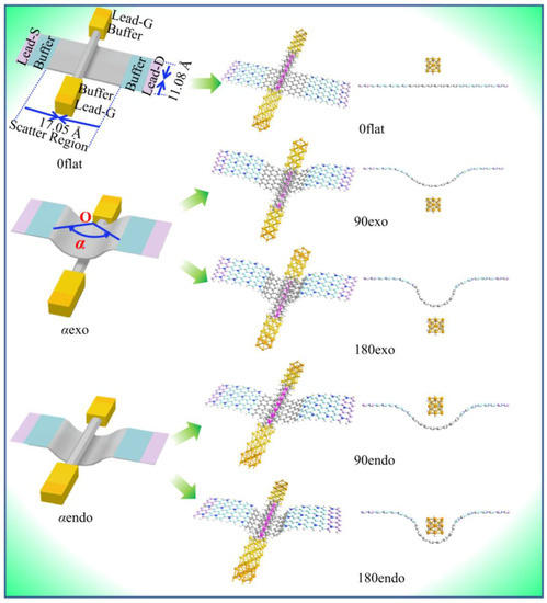
Figure 1.
The schematic plots of the four-terminal V7(Bz)8-WGNR devices.
2.2. Computational Details
The geometries of flat GNR with two N-doped GNR electrodes and V7Bz8 were optimized separately by utilizing DFT, as implemented in the Vienna ab initio simulation package (VASP). Then, the distance between the flat GNR and V7Bz8 was optimized by fixing their optimized structures. A projector-augmented wave basis set was employed with a cutoff energy of 300 eV. In the iterative calculation, the energy and force converged values were set as 10−4 eV and 0.05 eV·Å−1, respectively. To shield the interaction between the periodic images, the vacuum slab was set as 20 Å. The optimized value was 1.95 Å. Furthermore, based on the optimized geometry of the flat GNR, we constructed the WGNR structures with different curvatures. To qualitatively compare the influence of different bending curvatures on the transport properties of these four-terminal devices, the distances between WGNR and V7(Bz)8 were set as the same as that between the flat GNR and V7Bz8 (1.95 Å) for all the models. The distance between the Au electrode and V7Bz8 was also optimized by fixing their atoms positions. The optimized nearest S-Au distance is 2.34 Å, closing to their covalent bonding (2.39 Å) [60].
Transport properties of the five four-terminal conformations were calculated by using Nanodcal software package (Nanodcal 2019B) employing the DFT-NEGF method. In our simulation, the standard nonlocal norm-conserving pseudopotentials were used to describe the atomic core, while the double-zeta polarized (DZP) basis set was set for explaining the valence electronic orbitals. The exchange-correlation function was managed by the local density approximation (LDA) [61,62]. To confirm the reliability of the LDA results, we also carried out generalized gradient-approximation (GGA) calculations on the transport properties for the 0flat device at VS = 0.0 V. The computed conductance, current, and transmission of S-D channel with the variation of VG are shown in Figures S1–S3 in the Supporting Information. Clearly, the curves of these results exhibit a similar changing trend as varying VG for both LDA and GGA. This means that LDA and GGA could give the same evaluation of the gate influence on S-D channel. Therefore, the use of LDA to calculate the transport properties for all the designed four-terminal systems is appropriate. The Brillouin zone was integrated using the Monkhorst–Pack method, while k-points were set as 1 × 1 × 100 and 100 × 1 × 1 for source-to-drain channel leads and gate channels leads, respectively, as well as that for central region was 1 × 1 × 1. Notably, the spin state of V atoms was considered in all cases. And U-J was set to 3.4 eV [56] for the LDA + U scheme, which was employed to elucidate the on-site correlation effects among the 3d electrons of the V atom [62]. In addition, the energy and force convergence tolerance of self-consistent calculations were set as less than 10−4 eV and 0.05 eV/Å, respectively.
The spin-dependent current of the α-lead in a multi-terminal system can be evaluated using the Landauer–Büttiker formula [63,64]:
where Vα (Vβ) and fα (fβ) denote the electron potentials and the Fermi distribution functions of the α-lead (β-lead), respectively. Tαβ presents the transmission coefficient between α-and β-leads. σ is the spin index, ↑ (up-spin) and ↓ (down-spin). The total current is the sum of I↑ and I↓.
The conductance Gαβ is related to Tαβ, which can be obtained by the following formula:
3. Results and Discussions
The configurations of vdWHs devices of 0flat, 90exo, 180exo, 90endo, and 180endo are presented in Figure 1. In the forthcoming presentations, the gate-tuned transport properties of V7(Bz)8-WGNR devices were detected by evaluating the conductance, spin currents, transmission, local density of states, and scattering states. The source voltages (VS) were chosen as 0.0, 0.2, and 0.4 V. At a given Vs, the gate voltages (VG) were selected as 0.0, 0.2, 0.6, and 1.0 V.
The conductance as a function of VG at a fixed VS (VS = 0.0, 0.2, and 0.4 V) of all channels in the five four-terminal devices is shown in Figure 2. The conductance was in the range of 0.9–1.5 e2/h for the SD-channel, while it went down to 0.5–0.9 e2/h for the GG-channel. Such a difference derives from the fact that graphene possesses a metallic characteristic while V7(Bz)8 has a half-metallic feature. The conductance for SG- and DG-channels is always below 0.15 e2/h. The V7(Bz)8 attaches to graphene merely via a vdW interaction, so an unstraight way for carrier transporting along SG- and DG-channels is generated, leading the weaker conductivity. It is worth noting that, in the 0flat device, the conductance for SG- and DG-channels is almost zero in all cases, indicating that the channels between V7(Bz)8 and graphene are nearly closed. Clearly, the conductance does not always obey Ohm’s law, it sometimes oscillates with the variation of VG. Overall, with the growing VG, the conductance magnitude of SG-, and DG-channels is suppressed because of the stronger confrontation of gate potential against source potential. Simultaneously, the conductance of the SD-channel always goes up and down. Based on these results, it can be concluded that the change of VG can strongly influence the resistance in these channels, i.e., the precise regulation of conductance can be realized by varying VG.
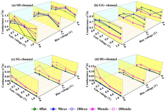
Figure 2.
Conductance of (a) SD-, (b) GG-, (c) SG-, and (d) DG-channels with various VG at a constant VS = 0.0, 0.2, or 0.4 V in the four-terminal V7(Bz)8-WGNR devices.
Furthermore, the conductance of SD-, SG-, and DG-channels in an endo-device is larger than that of the corresponding exo-device (pink lines vs. blue lines of Figure 2), especially that of SG-, and DG-channels. The gate and source potentials couple stronger in endo-devices, owing to the larger contact area between V7(Bz)8 and graphene. Accordingly, a counteractive effect is observed for GG-channel; that is, the conductance is smaller in endo-devices than that in exo-devices. Therefore, different position of V7(Bz)8 can bring about different coupling between V7(Bz)8 and WGNR. Meanwhile, the bending curvature also impacts the electronic properties as it can induce localization or delocalization in the electron state. This change in the charge distribution may result in modifications of conductance. Evidently, the bending curvature has a slight effect on the conductance of endo- and exo-devices which makes the values go a little up or down, depending on the complex potential couplings between these channels as well as their intrinsic electronic properties.
It is well known that V7(Bz)8 is a half-metallic conductor which is dominated solely by the down-spin channel. The up-spin and down-spin currents of each lead in the five four-terminal devices were computed to examine the gate-tuning effect of V7(Bz)8 on the transport property. For simplicity, the symbol IS↑ and IS↓ are used to signify the up- and down-spin current crossing the S-lead, respectively, while ID↑ and ID↓ as well as IG↑ and IG↓ are employed for those of the D-lead, and the G-lead, respectively. These values are given in Figure 3 varying with VG at each fixed VS. The value of the current flowing from the lead to the center region is positive, named input current, and that of the opposite direction is negative called output current. The colors of the current curves are black, red, and blue for VS = 0.0, 0.2, and 0.4V, respectively. Solid and dash lines are for up-spin and down-spin pathways, respectively. By comparing the curve shape of Figure 2 and Figure 3, it is readily observable that the shapes of S-lead and D-lead current curves are much more similar to the conductance curve of the SD-channel, indicating that the currents of S- and D-leads are stronger dependent on the current passing SD-channel. Actually, the current of each lead is always the sum of these from all its related channels. In addition, more complicated transport characteristics may be aroused by the mutual couplings between leads owing to the multi-terminal setup.
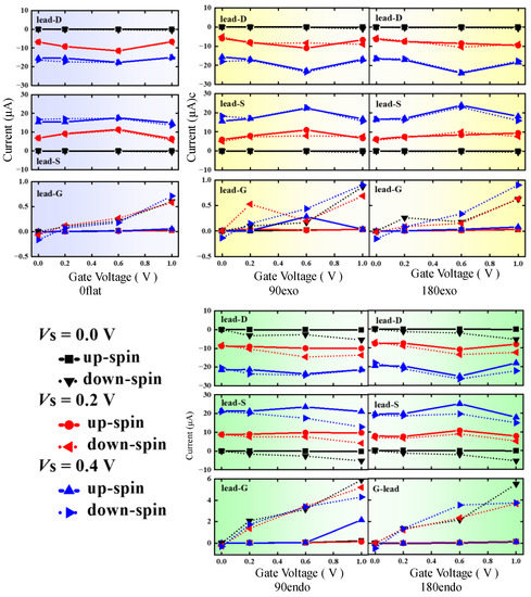
Figure 3.
Spin currents of S-, D-, and G-leads of the five four-terminal V7(Bz)8-WGNR devices with varying VG at a constant VS = 0.0, 0.2, and 0.4 V.
As anticipated, in V7(Bz)8, the magnitude of IG↓ is much higher than that of IG↑ originated from its native half-metallic behavior. However, such spin-polarized character has no significant effect on the electronic properties of 0flat, 90exo, and 180exo devices. This is due to the fact that the current of G-leads is an order of magnitude lower than that of S- and D-leads, i.e., the contact between V7(Bz)8 and WGNR in these systems is insufficient to induce noticeable perturbations by the applied gate voltages on the graphene main channel. However, the situation is different for 90endo and 180endo devices, where the polarized characteristic of V7(Bz)8 is almost completely imposed on the source-to-drain pathway, inducing striking polarized currents of S- and D-leads as well. Thus, the analysis mainly focuses on 90endo and 180endo devices in the following discussions.
Upon applying a higher VG, the currents across S- and D-leads are polarized to a larger extent. At VS = 0.0 V, S-lead exports only down-spin IS↓ which is driven by the spin-polarized gate voltage. Once VS is applied, currents IS↑ and IS↓ are both input currents while ID↑ and ID↓ are output currents. The curves of up-spin ID↑ and IS↑ are almost unchanged with the variation of the VG at a certain VS, which is mainly owing that VG and VS cannot activate the up-spin channel of V7(Bz)8 evidently in these situations, leading to scarcely any disturbance on the up-spin channel of WGNR.
Strong coupling occurs between the down-spin channels of V7(Bz)8 and WGNR, resulting in the splitting of up- and down-currents (see Figure 3). Evidently, the input IS↓ is always smaller than IS↑, while the output ID↓ is larger than ID↑. These results mean that the V7(Bz)8 tunes the spin-polarized transport properties of WGNR by importing the down-spin state carriers. The current IG↓ coming from V7(Bz)8 suppresses the input IS↓ leading to a smaller value compared with IS↑. On the contrary, down-spin current from V7(Bz)8 superimposes on the output magnitude of ID↓, and consequently, the spin-polarized current is generated by giving a larger ID↓ than ID↑. Such spin polarization becomes more obvious with the increasing of VG. The 90endo device produces a bit more evident splitting of the up- and down-current than the 180endo device. The bending curvature may be responsible for these phenomena: WGNR gives a smoother pathway in 90endo than in 180endo.
To make the transport property of the four-terminal V7(Bz)8-WGNR device more transparent, the transmission spectra (TS), which is dependent on the energy, was computed for the SD-channel. One can easily find evidence that the TS is closely related to the current based on the Landauer–Bütiker formula. Generally, the integral area of T (E, V) in the bias windows determines the current, where the bias window is referred to [−V/2, V/2] when the Fermi level is set to 0.0 eV. And the larger integral area exists, the higher current is. Figure 4 plots their TS at each applied VS when VG is fixed at 1.0 V for all the devices, where the pink region represents the bias window. For the 0flat device, there is almost no spin splitting in TS by tuning VS as shown in Figure 4a. However, by careful observation, one can find that the down-spin channels of exo- and endo-devices have a larger TS integral area in the bias window than the up-spin channels, and the spin splitting of 90exo and 90endo devices is more apparent than that of 180exo and 180endo devices. These results further confirm that the V7(Bz)8 can tune the down-spin transport properties of WGNR prominently by various VG. At the same time, the bending curvature and the position of V7(Bz)8 can also influence the down-spin state transport of WGNR.
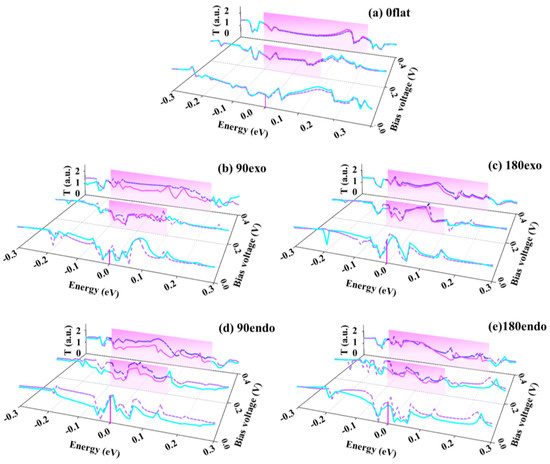
Figure 4.
Transmission spectra of the four-terminal V7(Bz)8-WGNR devices at VG = 1.0 V, where (a) is the TS for 0flat device, (b), (c), (d) and (e) are that for 90exo, 180exo, 90endo, 180endo devices, respectively. The solid lines represent the TS of the up-spin state, the dash lines that for the down-spin state. The magenta and bule lines denote the TS of up-spin and down-spin states in the bias window, respectively. The pink regions indicate the bias window.
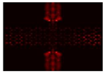
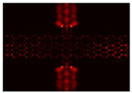
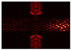
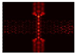
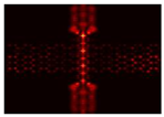
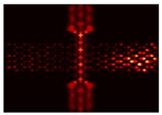
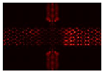
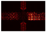
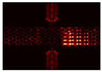
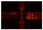
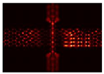
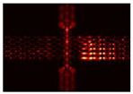
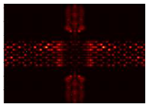
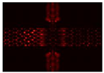
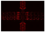
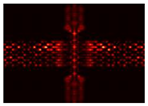
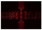
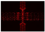
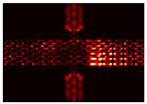
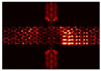
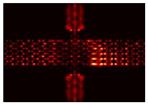
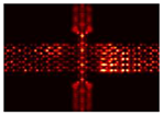
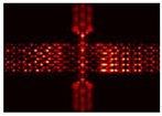
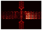
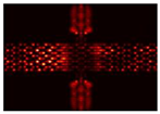
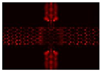
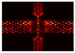
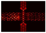
The distributions of the local density of states (LDOS) can also reveal the transport property of the four-terminal V7(Bz)8-WGNR devices. The diagrams of LDOS with various VS (0.0, 0.2, and 0.4V) at VG = 1.0 V are presented in Table 1. The change in the color of LDOS can give a sign of the change in the electronic potential distribution. Through comparative analyses of these figures, one can easily find that the distribution of the down-spin state LDOS of V7(Bz)8 is much more delocalized than that of the up-spin state. The down-spin channel of WGNR maybe perturbed by V7(Bz)8, which gives the reason to make a spin-polarized behavior of these four-terminal devices. Evidently, the VS, the bending curvature of WGNR, and the position of V7(Bz)8 all can tune the LDOS distribution of the whole system. The brighter LDOS color in the endo-devices than that in the exo-devices and 0flat device indicates that V7(Bz)8 has a stronger disturbance to WGNR in these cases, which explains why the polarized character is more outstanding in endo-devices in Figure 3. The scattering states of S- and D-leads in the four-terminal devices at VG = 1.0 V are summarized in Table 2 to further make the polarized transport character more patently. The charge carries through the up-spin channel are scattered stronger than that across the down-spin pathway. The polarized transport properties of WGNR are mainly induced by the tuning of the down-spin state of V7(Bz)8. It is worth noting that both the bending curvature of WGNR and the position of V7(Bz)8 could influence the polarized effect, especially, the 90endo-device shows the most obvious polarized characteristic.

Table 1.
Local density of states of the four-terminal V7(Bz)8-WGNR devices at various VS exemplified by VG = 1.0 V.

Table 2.
Scattering states of S-lead and D-lead at various VS in the four-terminal V7(Bz)8-WGNR devices exemplified by VG = 1.0 V.
4. Conclusions
Based on the DFT-NEGF method, the transport property of four-terminal V7(Bz)8-WGNR devices tuned by the polarized gate were investigated by analyzing the conductance, spin-polarized current, TS, LDOS, and scattering states. The results show that the position of V7(Bz)8, as well as the bending curvature of WGNR, can exert important influences on the transport property. The tuning effect of V7(Bz)8 mainly depends on its down-spin state, which can induce a spin-polarized transport property for these four-terminal devices. Particularly, the down-spin channel disturbs strongly on the source-to-drain conductance of WGNR when V7(Bz)8 is endo-positioned crossing the WGNR. We trust that these results could give guidance for designing flexible graphene-based electronic nanodevices by attaching other similar multidecker metal-arene nanowires.
Supplementary Materials
The following supporting information can be downloaded at: https://www.mdpi.com/article/10.3390/nano13152270/s1, Figure S1: Comparison of LDA and GGA calculated conductance of S-D channel at VS = 0.0 V for the 0flat device; Figure S2: Comparison of LDA and GGA calculated currents of S-lead and D-lead at VS = 0.0 V in the 0flat device; Figure S3: Comparison of LDA and GGA calculated transmission coefficient of S-D channel at VS = 0.0 V in the 0flat device.
Author Contributions
Conceptualization, H.Y. and G.Z.; data curation, H.Y. and G.Z.; funding acquisition, G.Z.; investigation, Y.S. and Y.H.; methodology, H.Y. and G.Z.; resources, G.Z.; validation, H.Y. and G.Z.; visualization, H.Y. and L.P.; writing—original draft, H.Y. and G.Z.; writing—review and editing, Y.S., Y.H. and G.Z. All authors have read and agreed to the published version of the manuscript.
Funding
This research was supported by Heilongjiang Provincial Natural Science Foundation of China, grant number ZD2023B001, and The APC was funded by No. ZD2023B001.
Data Availability Statement
The data presented in this study are available on request from the corresponding authors.
Conflicts of Interest
There are no conflict to declare.
References
- Klein, B.P.; Ihle, A.; Kachel, S.R.; Ruppenthal, L.; Hall, S.J.; Sattler, L.; Weber, S.M.; Herritsch, J.; Jaegermann, A.; Ebeling, D.; et al. Topological stone–wales defects enhance bonding and electronic coupling at the graphene/metal interface. ACS Nano 2022, 16, 11979–11987. [Google Scholar] [CrossRef]
- Loes, M.J.; Lipatov, A.; Vorobeva, N.S.; Lu, H.; Abourahma, J.; Muratov, D.S.; Gruverman, A.; Sinitskii, A. Enhanced photoresponse in few-layer SnS2 field-effect transistors modified with methylammonium lead iodide perovskite. ACS Appl. Electron. Mater. 2023, 5, 705–713. [Google Scholar] [CrossRef]
- Gudelli, V.K.; Alaal, N.; Roqan, I.S. Strain-engineering of electronic and magnetic properties of chemically passivated zigzag GaN nanoribbons: An Ab Initio Study. ACS Appl. Eng. Mater. 2023, 1, 1292–1300. [Google Scholar] [CrossRef]
- Kim, J.; Mastro, M.A.; Tadjer, M.J.; Kim, J. Heterostructure WSe2−Ga2O3 junction field-effect transistor for low-dimensional high-power electronics. ACS Appl. Mater. Interfaces 2018, 10, 29724–29729. [Google Scholar] [CrossRef]
- Zhou, J.; Li, H.; Tian, M.; Chen, A.; Chen, L.; Pu, D.; Hu, J.; Cao, J.; Li, L.; Xu, X.; et al. Multi-stimuli-responsive synapse based on vertical van der Waals heterostructures. ACS Appl. Mater. Interfaces 2022, 14, 35917–35926. [Google Scholar] [CrossRef]
- Papadopoulos, N.; Flores, E.; Watanabe, K.; Taniguchi, T.; Ares, J.R.; Sanchez, C.; Ferrer, I.J.; Castellanos-Gomez, A.; Steele, G.A.; van der Zant, H.S.J. Multi-terminal electronic transport in boron nitride encapsulated TiS3 nanosheets. 2D Mater. 2019, 7, 015009. [Google Scholar] [CrossRef]
- Fan, L.; Xu, J.; Hong, Y.H. Defects in graphene-based heterostructures: Topological and geometrical effects. RSC Adv. 2022, 12, 6772–6782. [Google Scholar] [CrossRef]
- Cheng, B.T.; Zhou, Y.; Jiang, R.M.; Wang, X.L.; Huang, S.; Huang, X.Y.; Zhang, W.; Dai, Q.; Zhou, L.J.; Lu, P.F.; et al. Structural, electronic and optical properties of some new trilayer Van de Waals heterostructures. Nanomaterials 2023, 13, 1574. [Google Scholar] [CrossRef]
- Wen, F.; Yuan, J.; Wickramasinghe, K.S.; Mayer, W.; Shabani, J.; Tutuc, E. Epitaxial Al-InAs heterostructures as platform for Josephson junction field-effect transistor logic devices. IEEE Trans. Electron Dev. 2021, 68, 1524–1529. [Google Scholar] [CrossRef]
- Feng, X.Q.; Liu, Z.D.; Zhang, G.L.; Zhang, S.; Huang, S.P.; He, Z.Y.; Wei, G.W.; Yang, S.W.; Zhu, Y.G.; Ye, C.C.; et al. Natural graphene plasmonic nano-resonators for highly active surface-enhanced raman scattering platforms. Energy Environ. Mater. 2022, 1–12. [Google Scholar] [CrossRef]
- Song, S.; Qiao, J.; Shen, M.Y.; Zhang, G.P.; Feng, F.; Somekh, M.G. Ultrasensitive photodetectors based on graphene quantum dot-InSe mixed-dimensional van der Waals heterostructures. J. Mater. Chem. C 2022, 10, 18174–18181. [Google Scholar] [CrossRef]
- Li, Z.L.; Guo, S.; Weller, D.; Quan, S.F.; Yu, J.; Wang, R.Q.; Wu, M.X.; Jiang, J.; Wang, Y.Y.; Liu, R.B. Boosting Enhancement of the electron-phonon coupling in mixed dimensional CdS/graphene van der Waals heterojunction. Adv. Mater. Interfaces 2022, 9, 2101893. [Google Scholar] [CrossRef]
- Wang, Y.; Xu, W.; Zhang, Y.; Zeng, C.X.; Zhang, W.N.; Fu, L.; Sun, M.; Wu, Y.Z.; Hao, J.; Zhong, W.; et al. Introducing spin polarization into mixed-dimensional van der waals heterostructures for high-efficiency visible-light photocatalysis. Energy Environ. Mater. 2022, 1–9. [Google Scholar] [CrossRef]
- Matsyshyn, O.; Xiong, Y.; Arora, A.; Song, J.C.W. Layer photovoltaic effect in van der Waals heterostructures. Phys. Rev. B 2023, 107, 205306. [Google Scholar] [CrossRef]
- Kakkar, S.; Majumdar, A.; Ahmed, T.; Parappurath, A.; Gill, N.K.; Watanabe, K.; Taniguchi, T.; Ghosh, A. High-efficiency infrared sensing with optically excited graphene-transition metal dichalcogenide heterostructures. Small 2022, 18, 2202626. [Google Scholar] [CrossRef]
- Wang, P.Q.; Jia, C.C.; Huang, Y.; Duan, X.F. Van der Waals heterostructures by design: From 1D and 2D to 3D. Matter 2021, 4, 552–581. [Google Scholar] [CrossRef]
- Wu, H.H.; Liu, X.C.; Zhu, K.Y.; Huang, Y. Fano resonance in near-field thermal radiation of two-Dimensional Van der Waals heterostructures. Nanomaterials 2023, 13, 1425. [Google Scholar] [CrossRef]
- Ye, F.; Islam, A.; Wang, Y.; Guo, J.; Feng, P.X.-L. Phase transition of MoTe2 controlled in van der Waals heterostructure nanoelectromechanical systems. Small 2023, 19, e2205327. [Google Scholar] [CrossRef]
- Sulleiro, M.V.; Develioglu, A.; Quiros-Ovies, R.; Martin-Perez, L.; Sabanes, N.M.; Gonzalez-Juarez, M.L.; Gomez, I.J.; Vera-Hidalgo, M.; Sebastian, V.; Santamaria, J. Fabrication of devices featuring covalently linked MoS2-graphene heterostructures. Nat. Chem. 2022, 14, 695. [Google Scholar] [CrossRef]
- Belete, M.; Engström, O.; Vaziri, S.; Lippert, G.; Lukosius, M.; Kataria, S.; Lemme, M.C. Electron Transport across vertical silicon/MoS2/graphene heterostructures: Towards efficient emitter diodes for graphene base hot electron transistors. ACS Appl. Mater. Interfaces 2020, 12, 9656–9663. [Google Scholar] [CrossRef]
- Wang, H.D.; Gao, S.; Zhang, F.; Meng, F.X.; Guo, Z.N.; Cao, R.; Zeng, Y.H.; Zhao, J.L.; Chen, S.; Hu, H.G.; et al. Repression of Interlayer Recombination by Graphene Generates a Sensitive Nanostructured 2D vdW Heterostructure ased Photodetector. Adv. Sci. 2021, 8, 2100503. [Google Scholar] [CrossRef]
- Liao, L.; Lin, Y.C.; Bao, M.; Cheng, R.; Bai, J.; Liu, Y.; Qu, Y.; Wang, K.L.; Huang, Y.; Duan, X. High-speed graphene transistors with a self-aligned nanowire gate. Nature 2010, 467, 305. [Google Scholar] [CrossRef]
- Liao, L.; Bai, J.; Qu, Y.; Lin, Y.C.; Li, Y.; Huang, Y.; Duan, X. High-kappa oxide nanoribbons as gate dielectrics for high mobility top-gated graphene transistors. Proc. Natl. Acad. Sci. USA 2010, 107, 6711–6715. [Google Scholar] [CrossRef]
- Liu, M.X.; Xue, Z.M.; Wang, Y.F.; Li, X.D.; Wang, C.G. Lateral constrained wrinkling of the film with partial contact. Int. J. Mech. Sci. 2022, 217, 107022. [Google Scholar] [CrossRef]
- Wimalananda, M.D.S.L.; Kim, J.K.; Lee, J.M. Characteristics of highly area-mismatched graphene-to-substrate transfers and the predictability of wrinkle formation in graphene for stretchable electronics. Adv. Mater. 2020, 7, 2001224. [Google Scholar] [CrossRef]
- Segawa, Y.; Yamazaki, K.; Yamasaki, J.; Gohara, K. Quasi-static 3D structure of graphene ripple measured using aberration-corrected TEM. Nanoscale 2021, 13, 5847–5856. [Google Scholar] [CrossRef]
- Banerjee, R.; Granzier-Nakajima, T.; Lele, A.; Schulze, J.A.; Hossain, M.J.; Zhu, W.B.; Pabbi, L.; Kowalik, M.; Duin, A.C.T.; Terrones, M.; et al. On the Origin of Nonclassical Ripples in Draped Graphene Nanosheets: Implications for Straintronics. ACS Appl. Nano Mater. 2022, 5, 10829–10838. [Google Scholar] [CrossRef]
- Li, Y.L.; Liu, X.Y.; Chen, C.H.; Duchamp, J.; Huang, R.; Chung, T.F.; Young, M.; Chalal, T.; Chen, Y.P.; Heflin, J.R.; et al. Differences in self-assembly of spherical C-60 and planar PTCDA on rippled graphene surfaces. Carbon 2019, 145, 549–555. [Google Scholar] [CrossRef]
- Min-Dianey, K.A.A.; Le, T.K.; Qadir, A.; M’Bouana, N.L.P.; Malik, M.; Kim, S.W.; Choi, J.R.; Pham, P.V. The ripple effect of graphite nanofilm on stretchable polydimethylsiloxane for optical sensing. Nanomaterials 2021, 11, 2934. [Google Scholar] [CrossRef]
- Sun, P.Z.; Xiong, W.Q.; Bera, A.; Timokhin, I.; Wu, Z.F.; Mishchenko, A.; Sellers, M.C.; Liu, B.L.; Cheng, H.M.; Janzen, E.; et al. Unexpected catalytic activity of nanorippled graphene. Proc. Natl. Acad. Sci. USA 2022, 120, e2300481120. [Google Scholar] [CrossRef]
- Hou, Y.T.; Stehle, R.C.; Qing, F.Z.; Li, X.S. Co-localized characterization of aged and transferred CVD graphene with scanning electron microscopy, atomic force microscopy, and raman spectroscopy. Adv. Mater. Technol. 2023, 8, 2200596. [Google Scholar] [CrossRef]
- Yildiz, G.; Bolton-Warberg, M.; Awaja, F. Graphene and graphene oxide for bio-sensing: General properties and the effects of graphene ripples. Acta Biomater. 2021, 131, 62–79. [Google Scholar] [CrossRef] [PubMed]
- Manno, D.; Torrisi, L.; Silipigni, L.; Buccolieri, A.; Cutroneo, M.; Torrisi, A.; Calcagnile, L.; Serra, A. From GO to rGO: An analysis of the progressive rippling induced by energetic ion irradiation. Appl. Surf. Sci. 2022, 586, 152789. [Google Scholar] [CrossRef]
- Sun, R.X.; Guo, Q.Q.; Huo, C.F.; Yan, X.Q.; Liu, Z.B.; Tian, J.G. Latest strategies for rapid and point of care detection of mycotoxins in food: A review. ACS Appl. Mater. Interfaces 2021, 13, 21573–21581. [Google Scholar] [CrossRef] [PubMed]
- Nikolaievskyi, D.; Torregrosa, M.; Merlen, A.; Clair, S.; Chuzel, O.; Parrain, J.L.; Neisus, T.; Campos, A.; Cabie, M.; Martin, C.; et al. Wrinkling and crumpling in twisted few and multilayer CVD graphene: High density of edge modes influencing Raman spectra. Carbon 2023, 203, 650–660. [Google Scholar] [CrossRef]
- Musikhin, S.; Talebi-Moghaddam, S.; Corbin, J.C.; Smallwood, G.J.; Schulz, C.; Daun, K.J. Crumpled few-layer graphene: Connection between morphology and optical properties. Carbon 2021, 182, 677–690. [Google Scholar] [CrossRef]
- Komlenok, M.; Kurochitsky, N.; Pivovarov, P.; Rybin, M.; Obraztsova, E. Field Electron Emission from Crumpled CVD Graphene Patterns Printed via Laser-Induced Forward Transfer. Nanomaterials 2022, 12, 1934. [Google Scholar] [CrossRef]
- Lee, M.J.; Lee, K.; Lim, J.; Li, M.C.; Noda, S.; Kwon, S.J.; DeMattia, B.; Lee, B.; Lee, S.W. Outstanding low-temperature performance of structure-controlled graphene anode based on surface-controlled charge storage mechanism. Adv. Funct. Mater. 2021, 31, 2009397. [Google Scholar] [CrossRef]
- Hu, K.M.; Liu, Y.Q.; Zhou, L.W.; Xue, Z.Y.; Peng, B.; Yan, H.; Di, Z.F.; Jiang, X.S.; Meng, G.; Zhang, W.M. Delamination-free functional graphene surface by multiscale, conformal wrinkling. Adv. Funct. Mater. 2020, 30, 2003273. [Google Scholar] [CrossRef]
- Li, Z.L.; Young, R.J.; Papageorgiou, D.G.; Kinloch, I.A.; Zhao, X.; Yang, C.; Hao, S.J. Interfacial stress transfer in strain engineered wrinkled and folded graphene. 2D Mater. 2019, 6, 045026. [Google Scholar] [CrossRef]
- Rhee, D.; Deng, S.K.; Odom, T.W. Soft skin layers for reconfigurable and programmable nanowrinkles. Nanoscale 2020, 12, 23920–23938. [Google Scholar] [CrossRef]
- Feng, L.C.; Chen, M.H.; Qian, Y.; Tian, J.W.; Liu, J.C.; Niu, S.; Muhammad, H.; Dong, M.D.; Zhong, J. Wrinkles with changing orientation and complexity in a single piece of thin film. J. Appl. Phys. 2019, 125, 245301. [Google Scholar] [CrossRef]
- Sampathkumar, K.; Androulidakis, C.; Koukaras, E.N.; Rahova, J.; Drogowska, K.; Kalbac, M.; Vetushka, A.; Fejfar, A.; Galiotis, C.; Frank, O. Sculpturing graphene wrinkle patterns into compliant substrates. Carbon 2019, 146, 772–778. [Google Scholar] [CrossRef]
- Kil, M.S.; Park, H.J.; Yoon, J.H.; Jang, J.W.; Lee, K.G.; Choi, B.G. Stretchable graphene conductor based on fluid dynamics and its application to flexible conductometric sensor. Carbon Lett. 2022, 32, 1791–1798. [Google Scholar] [CrossRef]
- Deng, S.K.; Berry, V. Wrinkled, rippled and crumpled graphene: An overview of formation mechanism, electronic properties, and applications. Mater. Today 2016, 19, 197–212. [Google Scholar] [CrossRef]
- Zhang, T.F.; Zhao, J.; Wang, Z.L.; Zhao, Y.X.; Wu, S.M.; Lai, L.M.; Li, M.J.; Jin, Y.H.; Wang, P.J.; Fan, S.S.; et al. Substrate engineering-tailored fabrication of aligned graphene nanoribbon arrays: Implications for graphene electronic devices. ACS Appl. Nano Mater. 2022, 4, 13838–13847. [Google Scholar] [CrossRef]
- Kumar, J.; Karthik, P.; Neppolian, B.; Thiruvadigal, D.J. Functionalization of zigzag graphene nanoribbon with DNA nucleobases-A DFT study. Appl. Surf. Sci. 2019, 496, 143667. [Google Scholar] [CrossRef]
- Houtsma, R.S.K.; de la Rie, J.; Stohr, M. Atomically precise graphene nanoribbons: Interplay of structural and electronic properties. Chem. Soc. Rev. 2021, 50, 6541–6568. [Google Scholar] [CrossRef] [PubMed]
- Chuan, M.W.; Lok, S.Z.; Hamzah, A.; Alias, N.E.; Sultan, S.M.; Lim, C.S.; Tan, M.L.P. Electronic properties of graphene nanoribbons with Stone-Wales defects using the tight-binding method. Adv. Nano Res. 2023, 14, 1–15. [Google Scholar] [CrossRef]
- Schneider, S.; Hoffmann-Vogel, R. Electrostatic forces above graphene nanoribbons and edges interpreted as partly hydrogen-free. Nanoscale 2020, 12, 17895–17901. [Google Scholar] [CrossRef]
- Zhang, S.H.; Chen, H.Y.; Hu, J.; Zhao, X.H.; Niu, X.B. First-principles calculations on lateral heterostructures of armchair graphene antidot nanoribbons for band alignment. ACS Appl. Nano Mater. 2022, 5, 5699–5708. [Google Scholar] [CrossRef]
- Pan, Z.H.; Liu, N.; Fu, L.; Liu, Z.F. Wrinkle engineering: A new approach to massive graphene nanoribbon arrays. J. Am. Chem. Soc. 2011, 133, 17578–17581. [Google Scholar] [CrossRef]
- Miyajima, K.; Yabushita, S.; Knickelbein, M.B.; Nakajima, A. Stern-gerlach experiments of one-dimensional metal-benzene sandwich clusters: Mn(C6H6)m(M=Al, Sc, Ti, and V). J. Am. Chem. Soc. 2007, 129, 8473–8480. [Google Scholar] [CrossRef] [PubMed]
- Yao, X.Y.; Zhang, X.Y.; Ye, X.Y.; Wang, J.L. Structure and electronic properties of bilayer graphene functionalized with half-sandwiched transition metal-cyclopentadienyl complexes. Phys. Chem. Chem. Phys. 2016, 18, 22390–22398. [Google Scholar] [CrossRef]
- Silva, W.R.; Cao, W.J.; Yang, D.S. Low-energy photoelectron imaging spectroscopy of Lan(Benzene) (n = 1 and 2). J. Phys. Chem. A 2017, 21, 8440–8447. [Google Scholar] [CrossRef] [PubMed]
- Pan, P.; Zhang, G.L.; Shang, Y.; Yang, Z.D.; Hu, Y.Y. (Bz)n and (VBz)n covalent functionalized MoS2 monolayer: Electronic and transport properties. Mater. Res. Express 2019, 6, 046304. [Google Scholar] [CrossRef]
- Gan, T.; Zhang, G.L.; Shang, Y.; Su, X.H.; Yang, Z.D.; Sun, X.J. Electronic and transport properties of the (VBz)n@MoS2NT nanocable. Phys. Chem. Chem. Phys. 2016, 18, 4385–4393. [Google Scholar] [CrossRef]
- Qu, L.T.; Liu, Y.; Baek, J.B.; Dai, L.M. Nitrogen-doped graphene as efficient metal-free electrocatalyst for oxygen reduction in fuel cells. ACS Nano 2010, 4, 1321–1326. [Google Scholar] [CrossRef]
- Wang, Y.X.; Jiang, Y.J.; Gao, S.N.; Yu, H.; Zhang, G.L.; Zhang, F.M. Tuning magnetism and transport property of planar and wrinkled FePP@GNR hybrid materials. AIP Adv. 2020, 10, 045112. [Google Scholar] [CrossRef]
- Kondoh, H.; Iwasaki, M.; Shimada, T.; Amemiya, K.; Yokoyama, T.; Ohta, T. Adsorption of thiolates to singly coordinated sites on Au(111) evidenced by photoelectron diffraction. Phys Rev Lett 2003, 90, 066102. [Google Scholar] [CrossRef]
- Yang, Y.; Han, X.; Han, Y.; Gong, W.J. First-principle studies on electron transport properties in four-terminal MoS2 nanoribbons. Physica B 2019, 554, 90–96. [Google Scholar] [CrossRef]
- Junquera, J.; Paz, Ó.; Sánchez-Portal, D.; Artacho, E. Numerical Atomic Orbitals for Linear-scaling Calculations. Phys. Rev. B 2001, 64, 235111. [Google Scholar] [CrossRef]
- Büttiker, M.; Imry, Y.; Landauer, R.; Pinhas, S. Generalized Many-channel Conductance Formula with Application to Small Rings. Phys. Rev. B 1985, 31, 6207–6215. [Google Scholar] [CrossRef] [PubMed]
- Wang, H.; Zhou, J.; Liu, X.J.; Yao, C.B.; Li, H.; Niu, L.; Wang, Y.; Yin, H.T. Spin transport through a junction entirely consisting of molecules from first principles. Appl. Phys. Lett. 2017, 111, 172408. [Google Scholar] [CrossRef]
Disclaimer/Publisher’s Note: The statements, opinions and data contained in all publications are solely those of the individual author(s) and contributor(s) and not of MDPI and/or the editor(s). MDPI and/or the editor(s) disclaim responsibility for any injury to people or property resulting from any ideas, methods, instructions or products referred to in the content. |
© 2023 by the authors. Licensee MDPI, Basel, Switzerland. This article is an open access article distributed under the terms and conditions of the Creative Commons Attribution (CC BY) license (https://creativecommons.org/licenses/by/4.0/).
