
Overcoming the Fermi-Level Pinning Effect in the Nanoscale Metal and Silicon Interface


Abstract
1. Introduction
2. Materials and Methods
2.1. Device Fabrication
2.2. Device Characterization
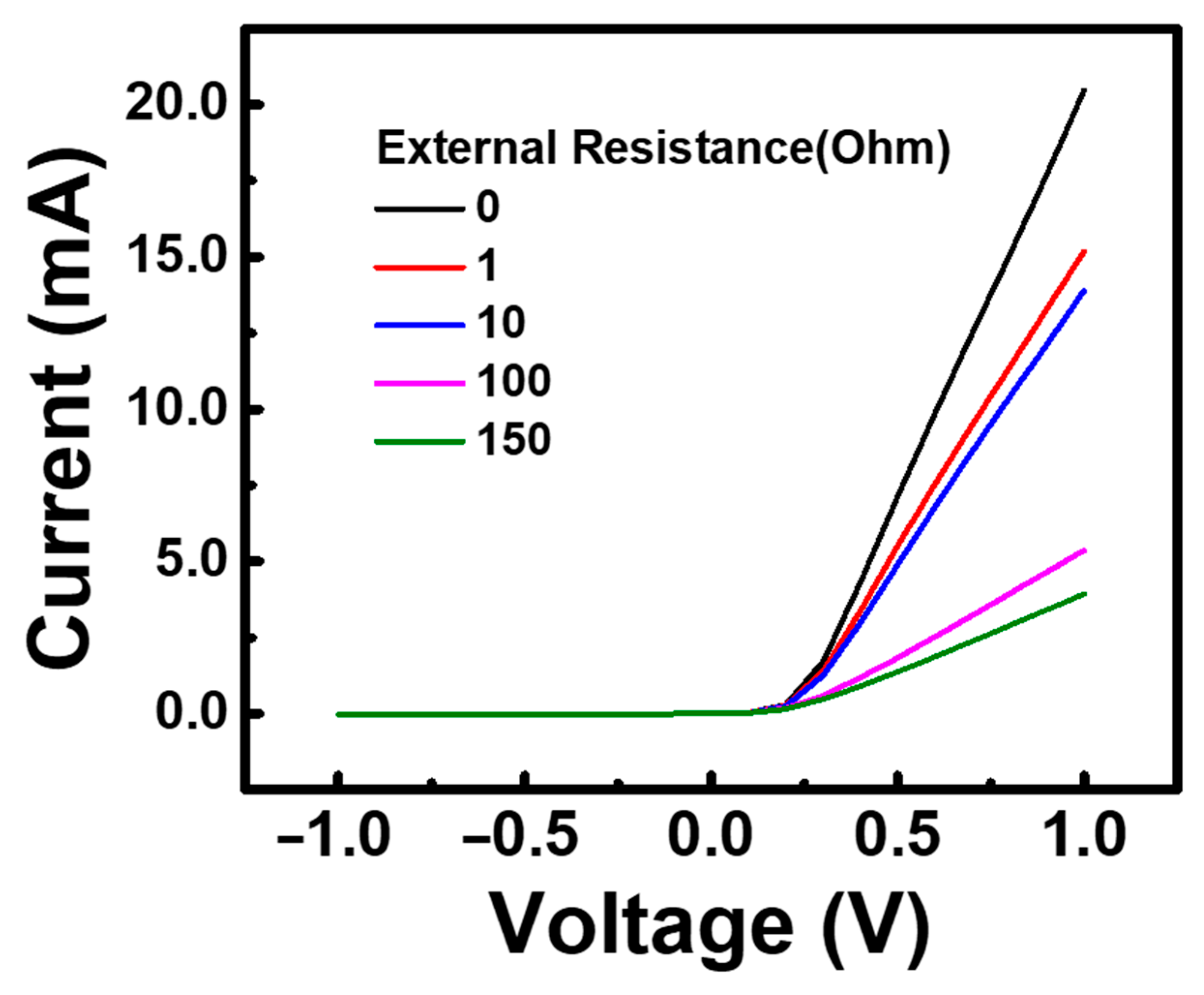
3. Results
4. Discussion
5. Conclusions
Author Contributions
Funding
Data Availability Statement
Acknowledgments
Conflicts of Interest
References
- Huang, T.; Fan, C.; Ma, L.; Zhang, X.; Fan, P.; Yang, Y.; Hu, W.; Zhou, H.; Zhuang, X.; Zhu, X.; et al. Single-crystalline InGaAs nanowires for room-temperature high-performance near-infrared photodetectors. Nano-Micro Lett. 2016, 8, 29–35. [Google Scholar]
- Miao, J.; Hu, W.; Guo, N.; Lu, Z.; Zou, X.; Liao, L.; Shi, S.; Chen, P.; Fan, Z.; Ho, J.C.; et al. Single InAs nanowire room-temperature near-infrared photodetectors. ACS Nano 2014, 8, 3628–3635. [Google Scholar] [CrossRef]
- Kuo, C.-H.; Wu, J.-M.; Lin, S.-J.; Chang, W.-C. High sensitivity of middle-wavelength infrared photodetectors based on an individual InSb nanowire. Nanoscale Res. Lett. 2013, 8, 327. [Google Scholar] [CrossRef] [PubMed]
- Shen, Y.; Li, Y.; Chen, W.; Jiang, S.; Li, C.; Cheng, Q. High-Performance Graphene Nanowalls/Si Self-Powered Photodetectors with HfO2 as an Interfacial Layer. Nanomaterials 2023, 13, 1681. [Google Scholar] [CrossRef] [PubMed]
- Li, G.; Maekita, K.; Mitsuno, H.; Maruyama, T.; Iiyama, K. Over 10 GHz lateral silicon photodetector fabricated on silicon-on-insulator substrate by CMOS-compatible process. Jpn. J. Appl. Phys. 2015, 54, 04DG06. [Google Scholar] [CrossRef]
- Liu, J.; Zhu, K.-M.; Zaslavsky, A.; Cristoloveanu, S.; Arsalan, M.; Wan, J. Photodiode with low dark current built in silicon-on-insulator using electrostatic doping. Solid-State Electron. 2020, 168, 107733. [Google Scholar] [CrossRef]
- Ghioni, M.; Zappa, F.; Kesan, V.; Warnock, J. A VLSI-compatible high-speed silicon photodetector for optical data link applications. IEEE Trans. Electron Devices 1996, 43, 1054–1060. [Google Scholar] [CrossRef]
- Liu, A.; Liao, L.; Rubin, D.; Nguyen, H.; Ciftcioglu, B.; Chetrit, Y.; Izhaky, N.; Paniccia, M. High-speed optical modulation based on carrier depletion in a silicon waveguide. Opt. Express 2007, 15, 660–668. [Google Scholar] [CrossRef]
- Casalino, M.; Coppola, G.; Iodice, M.; Rendina, I.; Sirleto, L. Near-infrared sub-bandgap all-silicon photodetectors: State of the art and perspectives. Sensors 2010, 10, 10571–10600. [Google Scholar] [CrossRef]
- Jalabert, R.; Das Sarma, S. Inelastic scattering in a doped polar semiconductor. Phys. Rev. B 1990, 41, 3651. [Google Scholar] [CrossRef]
- Petersen, C.L.; Lyon, S.A. Observation of hot-electron energy loss through the emission of phonon–plasmon coupled modes in GaAs. Phys. Rev. Lett. 1990, 65, 760. [Google Scholar] [CrossRef] [PubMed]
- Sicault, D.; Teissier, R.; Pardo, F.; Pelouard, J.-L.; Mollot, F. Experimental study of hot-electron inelastic scattering rate in p-type InGaAs. Phys. Rev. B 2002, 65, 121301. [Google Scholar] [CrossRef]
- Hilsum, C. Infrared absorption of thin metal films. J. Opt. Soc. Am. 1954, 44, 188–191. [Google Scholar] [CrossRef]
- Qi, Z.; Zhai, Y.; Wen, L.; Wang, Q.; Chen, Q.; Iqbal, S.; Chen, G.; Xu, J.; Tu, Y. Au nanoparticle-decorated silicon pyramids for plasmon-enhanced hot electron near-infrared photodetection. Nanotechnology 2017, 28, 275202. [Google Scholar] [CrossRef]
- Zhai, Y.; Li, Y.; Ji, J.; Wu, Z.; Wang, Q. Hot electron generation in silicon micropyramids covered with nanometer-thick gold films for near-infrared photodetectors. ACS Appl. Nano Mater. 2020, 3, 149–155. [Google Scholar] [CrossRef]
- Su, Z.-C.; Li, Y.-H.; Lin, C.-F. Mid-Infrared Response from Cr/n-Si Schottky Junction with an Ultra-Thin Cr Metal. Nanomaterials 2022, 12, 1750. [Google Scholar] [CrossRef]
- Sotthewes, K.; Van Bremen, R.; Dollekamp, E.; Boulogne, T.; Nowakowski, K.; Kas, D.; Zandvliet, H.J.W.; Bampoulis, P. Universal Fermi-level pinning in transition-metal dichalcogenides. J. Phys. Chem. C 2019, 123, 5411–5420. [Google Scholar] [CrossRef] [PubMed]
- Yuan, H.; Cheng, G.; You, L.; Li, H.; Zhu, H.; Li, W.; Kopanski, J.J.; Obeng, Y.S.; Walker, A.R.H.; Gundlach, D.J. Influence of Metal-MoS2 Interface on MoS2 Transistor Performance: Comparison of Ag and Ti Contacts. ACS Appl. Mater. Interfaces 2015, 7, 1180–1187. [Google Scholar] [CrossRef]
- Kim, C.; Moon, I.; Lee, D.; Choi, M.S.; Ahmed, F.; Nam, S.; Cho, Y.; Shin, H.-J.; Park, S.; Yoo, W.J. Fermi Level Pinning at Electrical Metal Contacts of Monolayer Molybdenum Dichalcogenides. ACS Nano 2017, 11, 1588–1596. [Google Scholar] [CrossRef]
- Zhang, Y.; Chen, X.; Zhang, H.; Wei, X.; Guan, X.; Wu, Y.; Wang, J. Fermi-level pinning mechanism in MoS2 field-effect transistors developed by thermionic emission theory. Appl. Sci. 2020, 10, 2754. [Google Scholar] [CrossRef]
- Sankey, F.; Allen, R.E.; Dow, J.D. Si/transition-metal Schottky barriers: Fermi-level pinning by Si dangling bonds at interfacial vacancies. Solid State Commun. 1984, 49, 1–5. [Google Scholar] [CrossRef]
- Khakbaz, P.; Driussi, F.; Giannozzi; Gambi, A.; Lizzit, D.; Esseni, D. Engineering of metal-MoS2 contacts to overcome Fermi level pinning. Solid-State Electron. 2022, 194, 108378. [Google Scholar] [CrossRef]
- Connelly, D.; Faulkner, C.; Clifton, A.; Grup, D.E. Fermi-level depinning for low-barrier Schottky source/drain transistors. Appl. Phys. Lett. 2006, 88, 012105. [Google Scholar] [CrossRef]
- Islam, R.; Shine, G.; Saraswat, K.C. Schottky barrier height reduction for holes by Fermi level depinning using metal/nickel oxide/silicon contacts. Appl. Phys. Lett. 2014, 105, 182103. [Google Scholar] [CrossRef]
- Kang, J.; Liu, W.; Sarkar, D.; Jena, D.; Banerjee, K. Computational study of metal contacts to monolayer transition-metal dichalcogenide semiconductors. Phys. Rev. X 2014, 4, 031005. [Google Scholar] [CrossRef]
- Park, I.; Lee, D.; Jin, B.; Kim, J.; Lee, J.-S. Improvement of Fermi-level pinning and contact resistivity in Ti/Ge contact using carbon implantation. Micromachines 2022, 13, 108. [Google Scholar] [CrossRef] [PubMed]
- Nazif, K.N.; Daus, A.; Hong, J.; Lee, N.; Vaziri, S.; Kumar, A.; Saraswat, K.C. High-specific-power flexible transition metal dichalcogenide solar cells. Nat. Commun. 2021, 12, 7034. [Google Scholar] [CrossRef]
- Elsmani, M.I.; Fatima, N.; Jallorina, M.P.A.; Sepeai, S.; Su’ait, M.S.; Ludin, N.A.; Teridi, M.A.M.; Sopian, K.; Ibrahim, M.A. Recent issues and configuration factors in perovskite-silicon tandem solar cells towards large scaling production. Nanomaterials 2021, 11, 3186. [Google Scholar] [CrossRef]
- Miao, J.; Zhang, X.; Tian, Y.; Zhao, Y. Recent Progress in Contact Engineering of Field-Effect Transistor Based on Two-Dimensional Materials. Nanomaterials 2022, 12, 3845. [Google Scholar] [CrossRef]
- Richstein, B.; Hellmich, L.; Knoch, J. Silicon nitride interface engineering for Fermi level depinning and realization of dopant-free MOSFETs. Micro 2021, 1, 228–241. [Google Scholar] [CrossRef]
- Yang, J.C.; Huang, H.F.; Li, J.H.; Lee, Y.J.; Wang, Y.H. Nitrogen plasma treatment of a TiO2 layer for MIS ohmic contact on n-type Ge substrate. Vacuum 2020, 171, 108996. [Google Scholar] [CrossRef]
- Shine, G.; Saraswat, K.C. Analysis of atomistic dopant variation and Fermi level depinning in nanoscale contacts. IEEE Trans. Electron Devices 2017, 64, 3768–3774. [Google Scholar] [CrossRef]
- Agrawal, A.; Lin, J.; Zheng, B.; Sharma, S.; Chopra, S.; Wang, K.; Datta, S. Barrier height reduction to 0.15 eV and contact resistivity reduction to 9.1 × 10⁻⁹ Ω-cm2 using ultrathin TiO2−x interlayer between metal and silicon. In Proceedings of the 2013 Symposium on VLSI Technology, Kyoto, Japan, 11–13 June 2013. [Google Scholar]
- Dev, S.; Meena, M.; Vardhan, H.; Lodha, S. Statistical simulation study of metal grain-orientation-induced MS and MIS contact resistivity variability for 7-nm FinFETs. IEEE Trans. Electron Devices 2018, 65, 3104–3111. [Google Scholar] [CrossRef]
- Zhang, T.; Raynaud, C.; Planson, D. Measure and analysis of 4H-SiC Schottky barrier height with Mo contacts. Eur. Phys. J. Appl. Phys. 2019, 85, 10102. [Google Scholar] [CrossRef]
- Orak, İ.; Kocyiğit, A.; Karataş, Ş. The analysis of the electrical and photovoltaic properties of Cr/p-Si structures using current-voltage measurements. Silicon 2018, 10, 2109–2116. [Google Scholar] [CrossRef]
- Bozhkov, V.G.; Torkhov, N.A.; Shmargunov, A.V. About the determination of the Schottky barrier height with the CV method. J. Appl. Phys. 2011, 109, 7. [Google Scholar] [CrossRef]
- Raynaud, C.; Isoird, K.; Lazar, M.; Johnson, C.M.; Wright, N. Barrier height determination of SiC Schottky diodes by capacitance and current-voltage measurements. J. Appl. Phys. 2002, 91, 9841–9847. [Google Scholar] [CrossRef]
- Khurelbaatar, Z.; Kil, Y.-H.; Yun, H.-J.; Shim, K.-H.; Nam, J.T.; Kim, K.-S.; Lee, S.-K.; Choi, C.-J. Modification of Schottky barrier properties of Au/n-type Ge Schottky barrier diode using monolayer graphene interlayer. J. Alloys Compd. 2014, 614, 323–329. [Google Scholar] [CrossRef]
- Bampoulis, P.; van Bremen, R.; Yao, Q.; Poelsema, B.; Zandvliet, H.J.W.; Sotthewes, K. Defect dominated charge transport and fermi level pinning in MoS2/metal contacts. ACS Appl. Mater. Interfaces 2017, 9, 19278–19286. [Google Scholar] [CrossRef]
- Schroder, D.K. Electrical characterization of defects in gate dielectrics. In Defects in Microelectronic Materials and Devices; Taylor & Francis Group: Abingdon, UK, 2009; pp. 119–163. [Google Scholar]
- Hung, K.K.; Cheng, Y.C. Process Dependence of the Si-SiO2 Interface Trap Density for Thin Oxides. J. Electrochem. Soc. 1987, 134, 2814. [Google Scholar] [CrossRef]
- Ji, C.H.; Kim, K.T.; Oh, S.Y. High-detectivity perovskite-based photodetector using a Zr-doped TiOx cathode interlayer. RSC Adv. 2018, 8, 8302–8309. [Google Scholar] [CrossRef] [PubMed]
- Wu, D.; Guo, J.; Wang, C.; Ren, X.; Chen, Y.; Lin, P.; Zeng, L.; Shi, Z.; Li, X.J.; Shan, C.-X.; et al. Ultrabroadband and high-detectivity photodetector based on WS2/Ge heterojunction through defect engineering and interface passivation. ACS Nano 2021, 15, 10119–10129. [Google Scholar] [CrossRef] [PubMed]
- Dou, L.; You, J.; Hong, Z.; Chang, W.-H.; Li, G.; Yang, Y. Solution-processed hybrid perovskite photodetectors with high detectivity. Nat. Commun. 2014, 5, 5404. [Google Scholar] [CrossRef] [PubMed]
- Yu, Y.Y.; Peng, Y.C.; Chiu, Y.C.; Liu, S.J.; Chen, C.P. Realizing Broadband NIR Photodetection and Ultrahigh Responsivity with Ternary Blend Organic Photodetector. Nanomaterials 2022, 12, 1378. [Google Scholar] [CrossRef]


| Rex (Ω) | 0 | 1 | 10 | 100 | 150 |
|---|---|---|---|---|---|
| Rs (Ω) | 29.92 | 31.00 | 40.152 | 131.120 | 181.033 |
| n | 1.492 | 1.496 | 1.495 | 1.498 | 1.496 |
| Barrier (eV) | 0.561 | 0.566 | 0.561 | 0.560 | 0.561 |
| T (K) | 300 | 298 | 298 | 298 | 298 |
| ΔRs (Ω) | 0.981 | 10.128 | 101.096 | 151.009 | |
| Relative Error (%) | 1.809 | 1.286 | 1.096 | 0.673 |
| Wavelength (nm) | 2000 | 3000 | 4000 | 5000 | 6000 |
|---|---|---|---|---|---|
| Response (nA) | |||||
| MS-0 s | 14.647 | 2.932 | |||
| MIS-30 s | 19.668 | 2.984 | |||
| MIS-60 s | 20.557 | 4.242 | 0.489 | 0.186 | 0.154 |
| MIS-120 s | 5.496 | 1.088 | |||
| MIS-180 s | 3.772 | 0.742 | |||
| MS | MIS-30 s | MIS-60 s | MIS-120 s | MIS-180 s | |
|---|---|---|---|---|---|
| Rs (Ω) | 29.924 | 38.210 | 20.294 | 25.194 | 27.243 |
| n | 1.492 | 1.773 | 1.97 | 3.127 | 3.267 |
| Barrier (eV) | 0.561 | 0.552 | 0.496 | 0.495 | 0.472 |
| Wavelength (nm) | Responsivity (nA/W) | D* (cmHz1/2W−1) |
|---|---|---|
| 2000 | 2.34 × 10⁵ | 1.17 × 10⁸ |
| 3000 | 4.82 × 10⁴ | 2.41 × 10⁷ |
| 4000 | 5.56 × 10³ | 2.78 × 10⁶ |
| 5000 | 2.11 × 10³ | 1.06 × 10⁶ |
| 6000 | 1.75 × 10³ | 8.75 × 10⁵ |
Disclaimer/Publisher’s Note: The statements, opinions and data contained in all publications are solely those of the individual author(s) and contributor(s) and not of MDPI and/or the editor(s). MDPI and/or the editor(s) disclaim responsibility for any injury to people or property resulting from any ideas, methods, instructions or products referred to in the content. |
© 2023 by the authors. Licensee MDPI, Basel, Switzerland. This article is an open access article distributed under the terms and conditions of the Creative Commons Attribution (CC BY) license (https://creativecommons.org/licenses/by/4.0/).
Share and Cite
Su, Z.-C.; Lin, C.-F. Overcoming the Fermi-Level Pinning Effect in the Nanoscale Metal and Silicon Interface. Nanomaterials 2023, 13, 2193. https://doi.org/10.3390/nano13152193
Su Z-C, Lin C-F. Overcoming the Fermi-Level Pinning Effect in the Nanoscale Metal and Silicon Interface. Nanomaterials. 2023; 13(15):2193. https://doi.org/10.3390/nano13152193
Chicago/Turabian StyleSu, Zih-Chun, and Ching-Fuh Lin. 2023. "Overcoming the Fermi-Level Pinning Effect in the Nanoscale Metal and Silicon Interface" Nanomaterials 13, no. 15: 2193. https://doi.org/10.3390/nano13152193
APA StyleSu, Z.-C., & Lin, C.-F. (2023). Overcoming the Fermi-Level Pinning Effect in the Nanoscale Metal and Silicon Interface. Nanomaterials, 13(15), 2193. https://doi.org/10.3390/nano13152193