
Solution-Grown MAPbBr3 Single Crystals for Self-Powered Detection of X-rays with High Energies above One Megaelectron Volt

 , , and
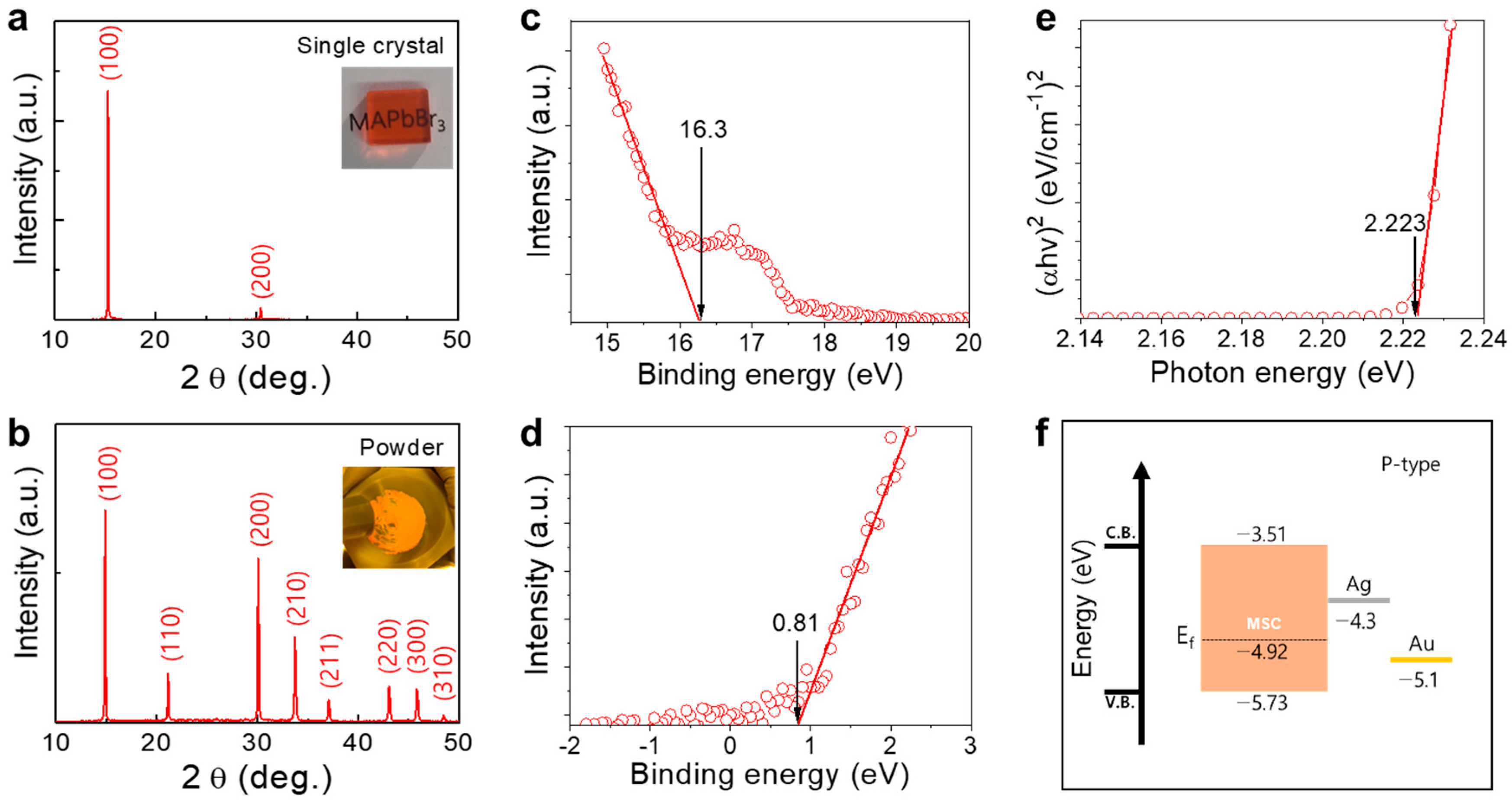
Abstract
1. Introduction
2. Materials and Methods
2.1. Growth of MSCs
2.2. Treatment of MSCs
2.3. Characterization of MSCs
2.4. Simulation and X-ray Evaluation of MSCs
3. Results and Discussion
3.1. MSC Characterization
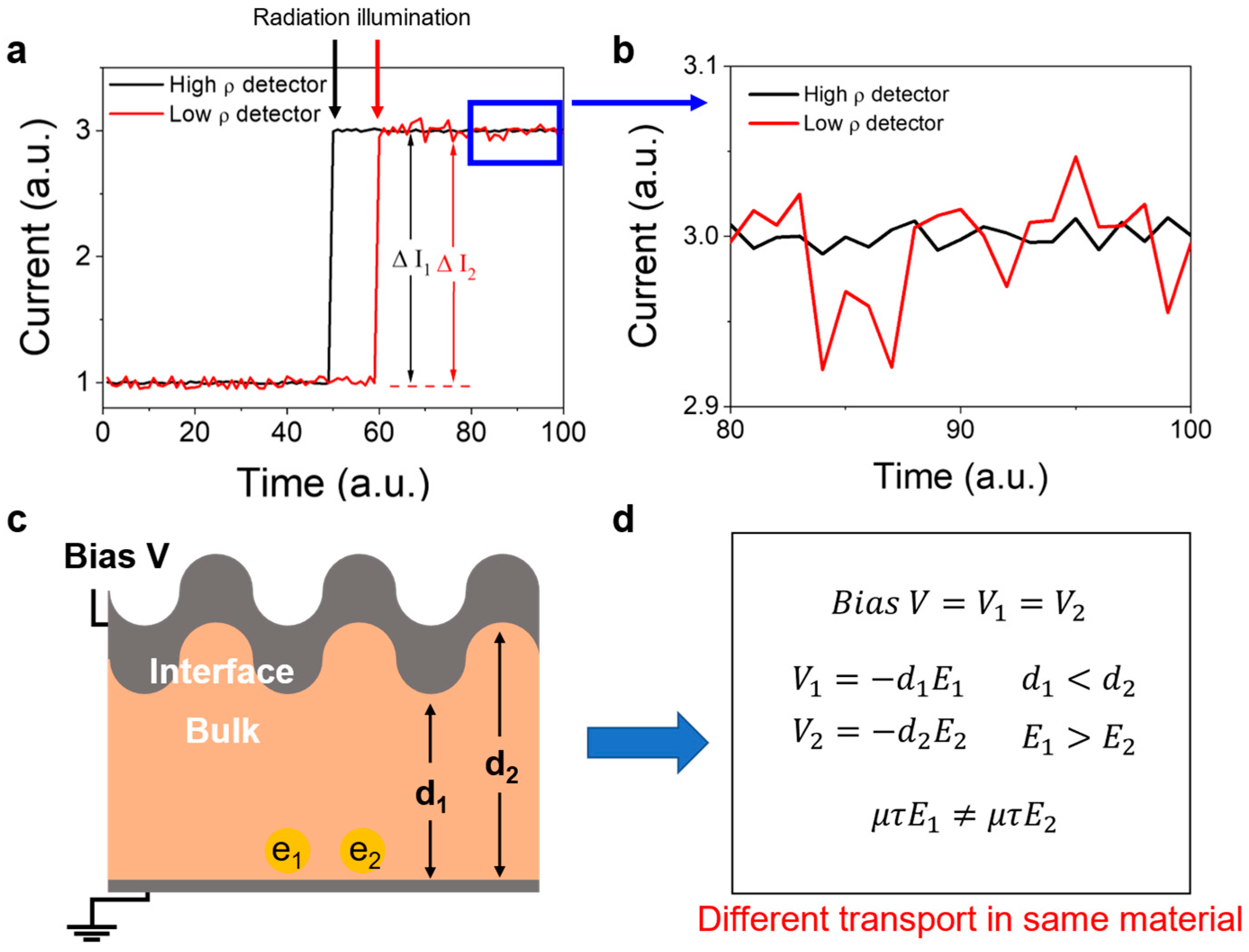
3.2. Effect of Surface State on Radiation Detector Performance
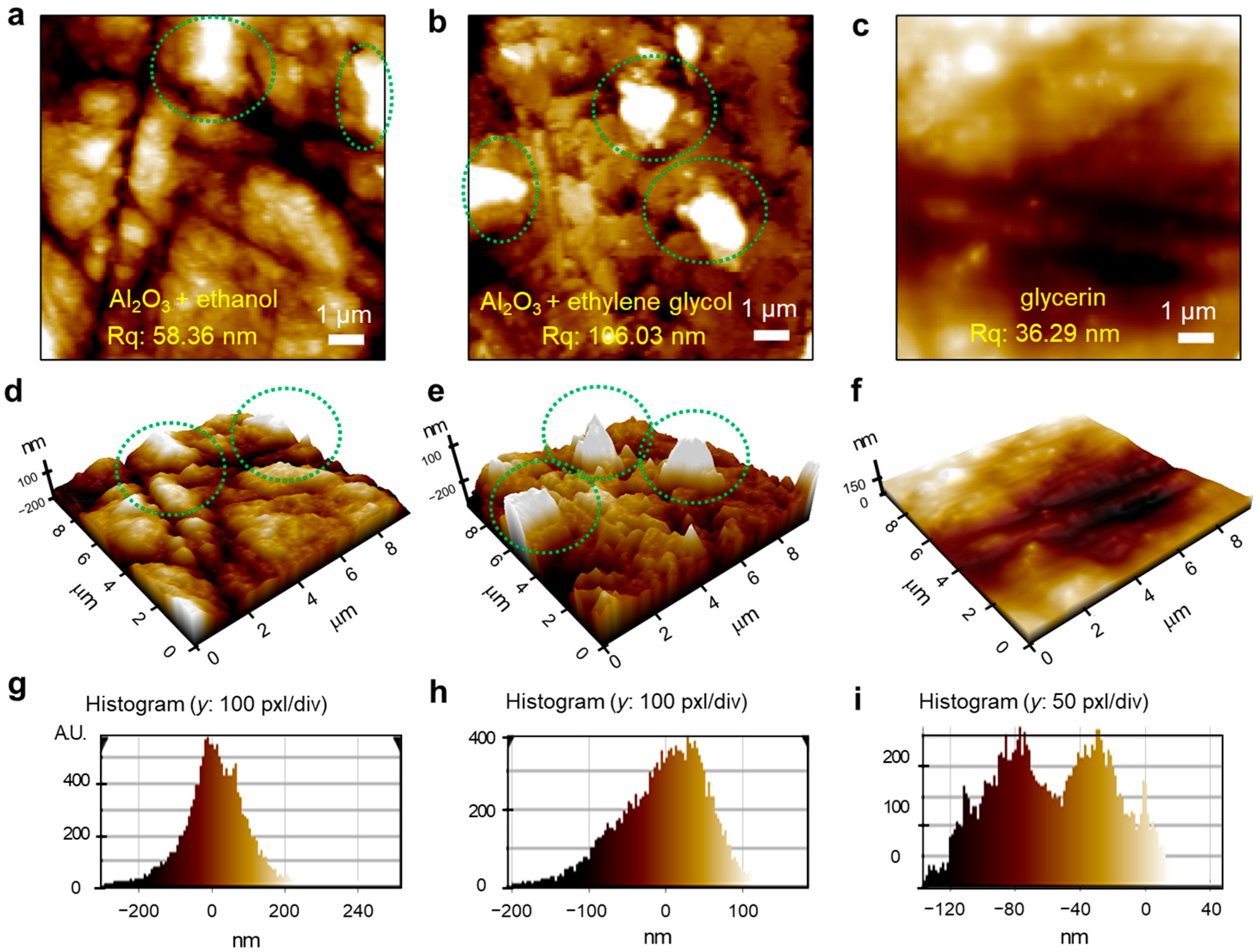
3.3. Enhancement of Defect, Transport, and Photocurrent Properties by Glycerin Polishing
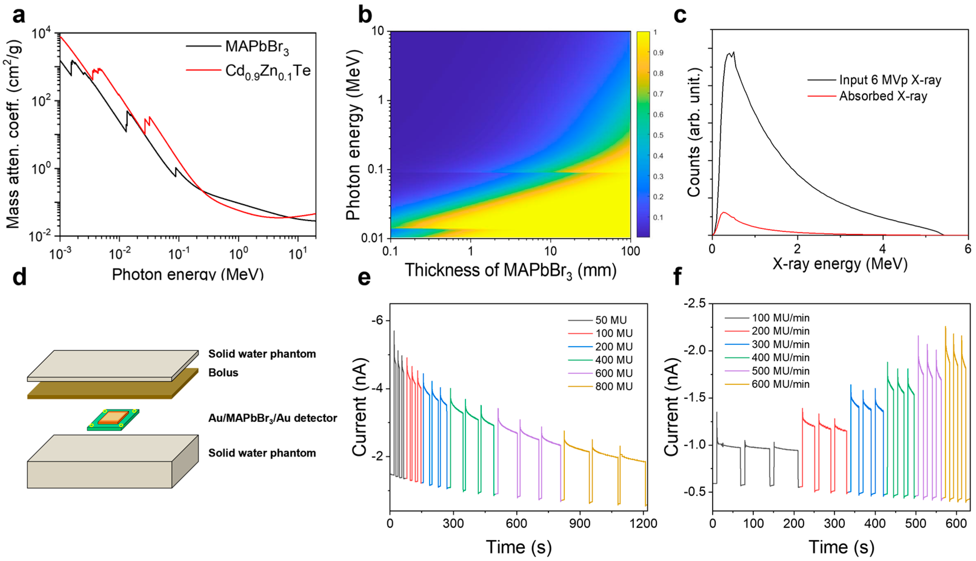
3.4. X-ray Sensitivity Evaluation
3.5. Megaelectron Volt X-ray Detection at a Zero Bias
4. Conclusions
Supplementary Materials
Author Contributions
Funding
Data Availability Statement
Conflicts of Interest
References
- Sakdinawat, A.; Attwood, D. Nanoscale X-ray imaging. Nat. Photonics 2010, 4, 840–848. [Google Scholar] [CrossRef]
- Tegze, M.; Faigel, G. X-ray holography with atomic resolution. Nature 1996, 380, 49–51. [Google Scholar] [CrossRef]
- Butson, M.J.; Rozenfeld, A.; Mathur, J.N.; Carolan, M.; Wong, T.P.Y.; Metcalfe, P.E. A new radiotherapy surface dose detector: The MOSFET. Med. Phys. 1996, 23, 655–658. [Google Scholar] [CrossRef] [PubMed]
- Kraushaar, W.L.; Clark, G.W.; Garmire, G.P.; Borken, R.; Higbie, P.; Leong, V.; Thorsos, T. High-Energy Cosmic Gamma-Ray Observations from the OSO-3 Satellite. Astrophys. J. 1972, 177, 341–363. [Google Scholar] [CrossRef]
- Knoll, G.F. Radiation Detection and Measurement, 4th ed.; John Wiley & Sons: Hoboken, NJ, USA, 2010; pp. 219–302. [Google Scholar]
- Chaudhuri, S.K.; Kleppinger, J.W.; Karadavut, O.; Nag, R.; Mandal, K.C. Quaternary Semiconductor Cd1−xZnxTe1−ySey for High-Resolution, Room-Temperature Gamma-Ray Detection. Crystals 2021, 11, 827. [Google Scholar] [CrossRef]
- Stoumpos, C.C.; Malliakas, C.D.; Peters, J.A.; Liu, Z.; Sebastian, M.; Im, J.; Chasapis, T.C.; Wibowo, A.C.; Chung, D.Y.; Freeman, A.J.; et al. Crystal growth of the perovskite semiconductor CsPbBr3: A new material for high-energy radiation detection. Cryst. Growth Des. 2013, 13, 2722–2727. [Google Scholar] [CrossRef]
- Yakunin, S.; Sytnyk, M.; Kriegner, D.; Shrestha, S.; Richter, M.; Matt, G.J.; Azimi, H.; Brabec, C.J.; Stangl, J.; Kovalenko, M.V.; et al. Detection of X-ray photons by solution-processed lead halide perovskites. Nat. Photonics 2015, 9, 444–449. [Google Scholar] [CrossRef]
- Wei, H.; Fang, Y.; Mulligan, P.; Chuirazzi, W.; Fang, H.-H.; Wang, C.; Ecker, B.R.; Gao, Y.; Loi, M.A.; Cao, L.; et al. Sensitive X-ray detectors made of methylammonium lead tribromide perovskite single crystals. Nat. Photonics 2016, 10, 333–339. [Google Scholar] [CrossRef]
- Stranks, S.D.; Eperon, G.E.; Grancini, G.; Menelaou, C.; Alcocer, M.J.P.; Leijtens, T.; Herz, L.M.; Petrozza, A.; Snaith, H.J. Electron-Hole Diffusion Lengths Exceeding 1 Micrometer in an Organometal Trihalide Perovskite Absorber. Science 2013, 342, 341–344. [Google Scholar] [CrossRef]
- Dong, Q.; Fang, Y.; Shao, Y.; Mulligan, P.; Qiu, J.; Cao, L.; Huang, J. Electron-hole diffusion lengths > 175 μm in solution-grown CH3NH3PbI3 single crystals. Science 2015, 347, 967–970. [Google Scholar] [CrossRef]
- Shi, D.; Adinolfi, V.; Comin, R.; Yuan, M.; Alarousu, E.; Buin, A.; Chen, Y.; Hoogland, S.; Rothenberger, A.; Katsiev, K.; et al. Low trap-state density and long carrier diffusion in organolead trihalide perovskite single crystals. Science 2015, 347, 519–522. [Google Scholar] [CrossRef] [PubMed]
- Wei, H.; DeSantis, D.; Wei, W.; Deng, Y.; Guo, D.; Savenije, T.J.; Cao, L.; Huang, J. Dopant compensation in alloyed CH3NH3PbBr3−xClx perovskite single crystals for gamma-ray spectroscopy. Nat. Mater. 2017, 16, 826–833. [Google Scholar] [CrossRef] [PubMed]
- Kasap, S.O. X-ray sensitivity of photoconductors: Application to stabilized a-Se. J. Phys. D Appl. Phys. 2000, 33, 2853–2865. [Google Scholar] [CrossRef]
- Li, L.; Liu, X.; Zhang, H.; Zhang, B.; Jie, W.; Sellin, P.J.; Hu, C.; Zeng, G.; Xu, Y. Enhanced X-ray Sensitivity of MAPbBr3 Detector by Tailoring the Interface-States Density. ACS Appl. Mater. Interfaces 2019, 11, 7522–7528. [Google Scholar] [CrossRef]
- Huang, Y.; Qiao, L.; Jiang, U.; He, T.; Long, R.; Yang, F.; Wang, L.; Lei, X.; Yuan, M.; Chen, J. A-site Cation Engineering for Highly Efficient MAPbI3 Single-Crystal X-ray Detector. Angew. Chem. Int. Ed. 2019, 58, 17834–17842. [Google Scholar] [CrossRef] [PubMed]
- Pan, W.; Yang, B.; Niu, G.; Xue, K.-H.; Du, X.; Yin, L.; Zhang, M.; Wu, H.; Miao, X.-S.; Tang, J. Hot-Pressed CsPbBr3 Quasi-Monocrystalline Film for Sensitive Direct X-ray Detection. Adv. Mater. 2019, 31, 1904405. [Google Scholar] [CrossRef]
- Zhuang, R.; Wang, X.; Ma, W.; Wu, Y.; Chen, X.; Tang, L.; Zhu, H.; Liu, J.; Wu, L.; Zhou, W.; et al. Highly sensitive X-ray detector made of layered perovskite-like (NH4)3Bi2I9 single crystal with anisotropic response. Nat. Photonics 2019, 13, 602–608. [Google Scholar] [CrossRef]
- Zhang, Y.; Liu, Y.; Xu, Z.; Ye, H.; Yang, Z.; You, J.; Liu, M.; He, Y.; Kanatzidis, M.G.; Liu, S.F. Nucleation-controlled growth of superior lead-free perovskite Cs3Bi2I9 single-crystals for high-performance X-ray detection. Nat. Commun. 2020, 11, 2304. [Google Scholar] [CrossRef]
- Morris, M.R.; Pendlebury, S.R.; Hong, J.; Dunn, S.; Durrant, J.R. Effect of Internal Electric Fields on Charge Carrier Dynamics in a Ferroelectric Material for Solar Energy Conversion. Adv. Mater. 2016, 28, 7123–7128. [Google Scholar] [CrossRef]
- Grinberg, I.; West, D.V.; Torres, M.; Gou, G.; Sein, D.M.; Wu, L.; Chen, G.; Gallo, E.M.; Akbashev, A.R.; Davies, P.K.; et al. Perovskite oxides for visible-light-absorbing ferroelectric and photovoltaic materials. Nature 2013, 503, 509–512. [Google Scholar] [CrossRef]
- Chen, Y.; Yi, H.T.; Wu, X.; Haroldson, R.; Gartstein, Y.N.; Rodionov, Y.I.; Tikhonov, K.S.; Zakhidov, A.; Zhu, X.-Y.; Podzorov, V. Extended carrier lifetimes and diffusion in hybrid perovskites revealed by Hall effect and photoconductivity measurements. Nat. Commun. 2016, 7, 12253. [Google Scholar] [CrossRef]
- Liu, X.; Wang, S.; Long, P.; Li, L.; Peng, Y.; Xu, Z.; Han, S.; Sun, Z.; Hong, M.; Luo, J. Polarization-Driven Self-Powered Photodetection in a Single-Phase Biaxial Hybrid Perovskite Ferroelectric. Angew. Chem. 2019, 131, 14646–14650. [Google Scholar] [CrossRef]
- Cao, F.; Tian, W.; Meng, L.; Wang, M.; Li, L. Ultrahigh-Performance Flexible and Self-Powered Photodetectors with Ferroelectric P(VDF-TrFE)/Perovskite Bulk Heterojunction. Adv. Funct. Mater. 2019, 29, 1808415. [Google Scholar] [CrossRef]
- Wang, S.; Li, L.; Weng, W.; Ji, C.; Liu, X.; Sun, Z.; Lin, W.; Hong, M.; Luo, J. Trilayered Lead Chloride Perovskite Ferroelectric Affording Self-Powered Visible-Blind Ultraviolet Photodetection with Large Zero-Bias Photocurrent. J. Am. Chem. Soc. 2020, 142, 55–59. [Google Scholar] [CrossRef] [PubMed]
- Heo, J.H.; Park, J.K.; Yang, Y.M.; Lee, D.S.; Im, S.H. Self-powered flexible all-perovskite X-ray detectors with high sensitivity and fast response. iScience 2021, 24, 102927. [Google Scholar] [CrossRef]
- Wu, J.; Wang, L.; Feng, A.; Yang, S.; Li, N.; Jiang, X.; Liu, N.; Xie, S.; Guo, X.; Fang, Y.; et al. Self-Powered FA0.55MA0.45PbI3 Single-Crystal Perovskite X-Ray Detectors with High Sensitivity. Adv. Funct. Mater. 2022, 32, 2109149. [Google Scholar] [CrossRef]
- Wei, H.; Huang, J. Halide lead perovskites for ionizing radiation detection. Nat. Commun. 2019, 10, 1066. [Google Scholar] [CrossRef]
- Sorde, S.D.; Abbene, L.; Caroli, E.; Mancini, A.M.; Zappettini, A.; Ubertini, P. Progress in the Development of CdTe and CdZnTe Semiconductor Radiation Detectors for Astrophysical and Medical Applications. Sensors 2009, 9, 3491–3526. [Google Scholar] [CrossRef]
- He, Y.; Stoumpos, C.C.; Hadar, I.; Luo, Z.; McCall, K.M.; Liu, Z.; Chung, D.Y.; Wessels, B.W.; Kanatzidis, M.G. Demonstration of Energy-Resolved γ-Ray Detection at Room Temperature by the CsPbCl3 Perovskite Semiconductor. J. Am. Chem. Soc. 2021, 143, 2068–2077. [Google Scholar] [CrossRef]
- Lu, H.; Zhang, H.; Yuan, S.; Wang, J.; Zhan, Y.; Zheng, L. An optical dynamic study of MAPbBr3 single crystals passivated with MAbCl3/I3-MAPbBr3 heterojunctions. Phys. Chem. Chem. Phys. 2017, 19, 4516–4521. [Google Scholar] [CrossRef]
- Zheng, Q.; Dierre, F.; Crocco, J.; Carcelen, V.; Bensalah, H.; Plaza, J.L.; Dieguez, E. Influence of surface preparation on CdZnTe nuclear radiation detectors. Appl. Surf. Sci. 2011, 257, 8742–8746. [Google Scholar] [CrossRef]
- Brovko, A.; Adelberg, A.; Chernyak, L.; Gorfman, S.; Ruzin, A. Impact of polishing on crystallinity and static performance of Cd1−xZnxTe. Nucl. Instrum. Methods Phys. Res. Sect. A Accel. Spectrometers Detect. Assoc. Equip. 2020, 984, 164568. [Google Scholar] [CrossRef]
- Xu, Q.; Shao, W.; Li, Y.; Zhang, X.; Ouyang, X.; Liu, J.; Liu, B.; Wu, Z.; Ouyang, X.; Tang, X.; et al. High-Performance Surface Barrier X-ray Detector Based on Methylammonium Lead Tribromide Single Crystals. ACS Appl. Mater. Interfaces 2019, 11, 9679–9684. [Google Scholar] [CrossRef] [PubMed]
- Wang, K.-H.; Li, L.-C.; Shellaiah, M.; Sun, K.W. Structural and Photophysical Properties of Methylammonium Lead Tribromide (MAPbBr3) Single Crystals. Sci. Rep. 2017, 7, 13643. [Google Scholar] [CrossRef]
- X-ray Mass Attenuation Coefficients. Available online: https://www.nist.gov/pml/x-ray-mass-attenuation-coefficients (accessed on 7 July 2023).
- Leyden, M.R.; Meng, L.; Jiang, Y.; Ono, L.K.; Qiu, L.; Juarez-Perez, E.J.; Qin, C.; Adachi, C.; Qi, Y. Methylammonium Lead Bromide Perovskite Light-Emitting Diodes by Chemical Vapor Deposition. J. Phys. Chem. Lett. 2017, 8, 3193–3198. [Google Scholar] [CrossRef]
- Chen, L.; Wang, H.; Zhang, W.; Li, F.; Wang, Z.; Wang, X.; Shao, Y.; Shao, J. Surface Passivation of MAPbBr3 Perovskite Single Crystals to Suppress Ion Migration and Enhance Photoelectronic Performance. ACS Appl. Mater. Interfaces 2022, 14, 10917–10926. [Google Scholar] [CrossRef]
- Hecht, K. Zum Mechanismus des lichtelektrischen Primärstromes in isolierenden Kristallen. Z. Phys. 1932, 77, 235–245. [Google Scholar] [CrossRef]
- Matz, R.; Weidner, M. Charge collection efficiency and space charge formation in CdTe gamma and X-ray detectors. Nucl. Instrum. Methods Phys. Res. Sect. A Accel. Spectrometers Detect. Assoc. Equip. 1998, 406, 287–298. [Google Scholar] [CrossRef]
- Byun, J.; Seo, J.; Seo, J.; Park, B. Growth and characterization of detector-grade CdMnTeSe. Nucl. Eng. Technol. 2022, 54, 4215–4219. [Google Scholar] [CrossRef]
- Herz, L.M. Charge-Carrier Mobilities in Metal Halide Perovskites: Fundamental Mechanisms and Limits. ACS Energy Lett. 2017, 2, 1539–1548. [Google Scholar] [CrossRef]
- Elbaz, G.A.; Straus, D.B.; Semonin, O.E.; Hull, T.D.; Paley, D.W.; Kim, P.; Owen, J.S.; Kagan, C.R.; Roy, X. Unbalanced Hole and Electron Diffusion in Lead Bromide Perovskites. Nano Lett. 2017, 17, 1727–1732. [Google Scholar] [CrossRef] [PubMed]
- Park, B.; Kim, Y.; Seo, J.; Byun, J.; Kim, K. Passivation effect on large volume CdZnTe crystals. Nucl. Eng. Technol. 2022, 54, 4620–4624. [Google Scholar] [CrossRef]
- Kamieniecki, E. Effect of charge trapping on effective carrier lifetime in compound semiconductors: High resistivity CdZnTe. J. Appl. Phys. 2014, 116, 193702. [Google Scholar] [CrossRef]
- He, Y.; Petryk, M.; Liu, Z.; Chica, D.G.; Hadar, I.; Leak, C.; Ke, W.; Spanopoulos, I.; Lin, W.; Chung, D.Y.; et al. CsPbBr3 perovskite detectors with 1.4% energy resolution for high-energy γ-rays. Nat. Photonics 2021, 15, 36–42. [Google Scholar] [CrossRef]
- Rodriguez, M.; Sempau, J.; Brualla, L. PRIMO: A graphical environment for the Monte Carlo simulation of Varian and Elekta linacs. Strahlenther. Onkol. 2013, 189, 881–886. [Google Scholar] [CrossRef] [PubMed]
- Khan, F.M. The Physics of Radiation Therapy, 4th ed.; Lippincott Williams & Wilkins: Philadelphia, PA, USA, 2010; Volume 137. [Google Scholar]


Disclaimer/Publisher’s Note: The statements, opinions and data contained in all publications are solely those of the individual author(s) and contributor(s) and not of MDPI and/or the editor(s). MDPI and/or the editor(s) disclaim responsibility for any injury to people or property resulting from any ideas, methods, instructions or products referred to in the content. |
© 2023 by the authors. Licensee MDPI, Basel, Switzerland. This article is an open access article distributed under the terms and conditions of the Creative Commons Attribution (CC BY) license (https://creativecommons.org/licenses/by/4.0/).
Share and Cite
Park, B.; Ko, J.; Byun, J.; Pandey, S.; Park, B.; Kim, J.; Lee, M.-J. Solution-Grown MAPbBr3 Single Crystals for Self-Powered Detection of X-rays with High Energies above One Megaelectron Volt. Nanomaterials 2023, 13, 2157. https://doi.org/10.3390/nano13152157
Park B, Ko J, Byun J, Pandey S, Park B, Kim J, Lee M-J. Solution-Grown MAPbBr3 Single Crystals for Self-Powered Detection of X-rays with High Energies above One Megaelectron Volt. Nanomaterials. 2023; 13(15):2157. https://doi.org/10.3390/nano13152157
Chicago/Turabian StylePark, Beomjun, Juyoung Ko, Jangwon Byun, Sandeep Pandey, Byungdo Park, Jeongho Kim, and Man-Jong Lee. 2023. "Solution-Grown MAPbBr3 Single Crystals for Self-Powered Detection of X-rays with High Energies above One Megaelectron Volt" Nanomaterials 13, no. 15: 2157. https://doi.org/10.3390/nano13152157
APA StylePark, B., Ko, J., Byun, J., Pandey, S., Park, B., Kim, J., & Lee, M.-J. (2023). Solution-Grown MAPbBr3 Single Crystals for Self-Powered Detection of X-rays with High Energies above One Megaelectron Volt. Nanomaterials, 13(15), 2157. https://doi.org/10.3390/nano13152157