Review

Advancing Thermoelectric Materials: A Comprehensive Review Exploring the Significance of One-Dimensional Nano Structuring

by
Mustafa Majid Rashak Al-Fartoos
,
Anurag Roy
*,
Tapas K. Mallick
and
Asif Ali Tahir
*
Solar Energy Research Group, Environment and Sustainability Institute, University of Exeter, Penryn Campus, Cornwall TR10 9FE, UK
*
Authors to whom correspondence should be addressed.
Nanomaterials 2023, 13(13), 2011; https://doi.org/10.3390/nano13132011
Submission received: 8 June 2023 / Revised: 29 June 2023 / Accepted: 2 July 2023 / Published: 5 July 2023

Abstract

:
Amidst the global challenges posed by pollution, escalating energy expenses, and the imminent threat of global warming, the pursuit of sustainable energy solutions has become increasingly imperative. Thermoelectricity, a promising form of green energy, can harness waste heat and directly convert it into electricity. This technology has captivated attention for centuries due to its environmentally friendly characteristics, mechanical stability, versatility in size and substrate, and absence of moving components. Its applications span diverse domains, encompassing heat recovery, cooling, sensing, and operating at low and high temperatures. However, developing thermoelectric materials with high-performance efficiency faces obstacles such as high cost, toxicity, and reliance on rare-earth elements. To address these challenges, this comprehensive review encompasses pivotal aspects of thermoelectricity, including its historical context, fundamental operating principles, cutting-edge materials, and innovative strategies. In particular, the potential of one-dimensional nanostructuring is explored as a promising avenue for advancing thermoelectric technology. The concept of one-dimensional nanostructuring is extensively examined, encompassing various configurations and their impact on the thermoelectric properties of materials. The profound influence of one-dimensional nanostructuring on thermoelectric parameters is also thoroughly discussed. The review also provides a comprehensive overview of large-scale synthesis methods for one-dimensional thermoelectric materials, delving into the measurement of thermoelectric properties specific to such materials. Finally, the review concludes by outlining prospects and identifying potential directions for further advancements in the field.

Graphical Abstract

1. Introduction

Climate change has caused considerably greater adverse impacts than previously anticipated by scientists a few years ago. This outcome stems from the rapid escalation in the utilization of fossil fuels to meet the surging demands of the residential, industrial, and transportation sectors. These demands have intensified in response to the rapid expansion of the global population, which surpassed 8 billion individuals in November 2022 [1]. In addition, the low energy efficiency of conventional sources has led to greater fuel consumption and a high carbon footprint. As a result, carbon dioxide emissions from fossil fuels are expected to rise by 1% worldwide in 2022 [2]. If this situation holds, humans will have produced enough CO2 in the atmosphere to cause global temperatures to rise by 1.5 °C above pre-industrial levels in just nine years [2]. The escalating need to mitigate CO2 emissions has amplified the call for alternative and sustainable energy sources. Numerous clean energy options exist, including solar, wind, geothermal, hydroelectric, and piezoelectric. Nonetheless, to effectively combat the adverse consequences of climate change, it has become imperative to harness the full spectrum of available green energy sources.
In the current era, the scientific community has directed its attention towards exploring alternative energy sources and enhancing energy conversion efficiency. Among the focus areas, thermoelectric (TE) materials have garnered significant interest. These materials are uniquely capable of directly converting heat into electricity, making them a promising candidate for clean energy applications. By harnessing waste heat from various energy generation systems, including renewable sources, TE materials offer the potential to reduce environmental pollution and enhance energy conversion efficiency. To illustrate this concept, consider the example of a conventional oil-based power generator, which typically exhibits an efficiency of only 30%. This means 70% of the chemical energy is dissipated as waste heat. However, by integrating a TE generator, the overall efficiency can be increased by approximately 2.5% by converting heat into usable electricity. Consequently, when a TE generator is attached to a fossil fuel generator, substantial annual savings of around $50,000 in fuel costs can be achieved, along with the mitigation of approximately 156 tons of CO2 emissions [3].
Therefore, using TE materials in energy conversion systems presents a significant opportunity to enhance sustainability and address the global energy crisis. By efficiently converting waste heat into valuable electrical energy, TE materials contribute to improving clean energy technologies and reducing greenhouse gas emissions.
TE devices made of TE materials are considered simple to operate, compact, silent, and durable, as there are no moving parts. These devices are reliable and have been used in many specialised industries, such as waste heat recovery from power plants [4] and automobiles, to reduce fuel consumption [5]; atomic batteries for power generation in the aerospace field [6]; wearable TE materials to harvest heat from the human body [7]; solar-thermoelectric generators (TEGs) applications [8]; sensors for medical applications [9]; and glazing for energy efficient buildings [10]. However, the poor efficiency of the currently available TE devices and the sustainability of state-of-the-art materials are holding back the wider usage of this technology [11].
TE technology should be capable of competing efficiently with current technologies to grow into non-niche applications [12]. The energy conversion efficiency of TE materials is mainly evaluated by a dimensionless TE figure of merit (ZT). ZT is defined by the equation Z T = S 2 σ k T where S, σ, k , T is the Seebeck coefficient, the electrical conductivity, thermal conductivity, and absolute temperature, respectively [13]. Therefore, ZT is inversely proportional to the thermal conductivity and directly proportional to the Seebeck coefficient and the electrical conductivity. ZT of at least 4 is necessary to compete on efficiency with other thermal-to-electric conversion technologies such as organic Rankine and Kalina cycles, where the efficiency of the conversion of heat into work for these cycles range from 40% to 50% [14].
TE materials with high-performance efficiency are often expensive to produce, contain toxic elements, and rely on rare-earth elements. Consequently, significant research focuses on developing low-cost, high-efficiency, and environmentally friendly TE materials derived from abundant elements. One-dimensional (1D) nanostructure TE materials have gained considerable attention from researchers worldwide due to their unique properties. Despite the abundance of review articles on TE materials, few specifically concentrate on 1D TE materials, as visually depicted in Figure 1. An extensive search using the keyword “thermoelectric” in the Web of Science database has yielded an astonishing number of articles (60,439), underscoring the consistent progress and advancements within this field concerning recent technological innovations. However, when focusing on the realm of 1D TE, the overall volume of research articles diminishes considerably to a mere 1445, in contrast to the broader category of TE.
Consequently, the primary objective of this review is to offer a more concentrated analysis of 1D TE, meticulously examining their prospects and appraising the notable innovations achieved thus far from an advanced technological standpoint. Figure 1 visually demonstrates the remarkable adaptability of 1D TE materials across various domains, with materials science and applied physics assuming principal roles as contributing disciplines. The graph illustrates the significant difference in the number of research publications dedicated to 1D TE compared to the broader field of TE.
Thus, comprehending the significance of 1D materials in practical applications becomes paramount, necessitating further investigation. This review endeavours to shed light on this captivating field’s fundamental aspects and future possibilities. It aims to fill that gap by providing a comprehensive overview of the history, fundamental principles, and recent advancements in TE materials. It critically evaluates various materials based on their chemical structures, efficiency, and physical properties and explores potential approaches to enhance their performance. Specifically, it extensively examines the impact of 1D nanostructuring as one of the most effective methods to enhance TE materials. Various configurations of 1D nanostructured TE materials are compared and analysed regarding their influence on TE parameters. Additionally, the paper highlights key large-scale synthesis methods for 1D nanostructure TE materials and discusses characterization techniques to evaluate their performance. Overall, this comprehensive overview serves as a valuable resource for materials scientists, chemists, physicists, and engineers, particularly young researchers, assisting them in making informed decisions regarding suitable materials for their applications and strategies for developing desired material properties.

1.1. Historical Background

Experiments by Italian scientists (Luigi Galvani and Alessandro Volta) at the end of the 18th century were the first evidence of the direct conversion between thermal and electrical energy [16]. In (1770–1831), the German physicist Thomas Johann Seebeck noticed that when a magnetic needle is brought near a circuit of two dissimilar metals with their connections maintained at different temperatures, it deflects the field [17]. This is because the temperature difference will force the charge to flow through the conductor, and this phenomenon is known as the Seebeck effect. In 1834, a French watchmaker and part-time physicist, Jean Peltier (1785–1845), discovered an alternative to the Seebeck effect in which the flow of an electric current caused temperature differences at the junction of two dissimilar metals, known as the Peltier effect [18]. William Thomson (1824–1907), often referred to as Lord Kelvin, was the first to link these two fundamental phenomena in 1851. The Seebeck coefficient multiplied by absolute temperature equals the Peltier coefficient; in his thermodynamic derivation, Thomson predicted that there would be a third TE effect, now known as the Thomson effect [19,20].
Edmund Altenkirch (1880–1953) proposed a theory for calculating the efficiency of TEGs in 1909 and the performance of a cooler in 1911, demonstrating that a suitable material should have a high Seebeck coefficient, high electrical conductivity, and low thermal conductivity. This relationship was later developed by Abram Fedorovich Ioffe (1880–1960) into the “figure of merit” ( Z T ) [19,21]. Maria Telkes (1900–1995) successfully constructed the first (solar) TE power generator in 1947 and the TE refrigerator in 1953 using semiconductor thermoelectricity principles. The average efficiency of 5% for Telkes’s generators was reached [22]. By the 1950s, cooling temperatures below 0 °C had been achieved by H. Julian Goldsmid and R. W. Douglas, enabling the development of several successful companies [19,20].
Glen Slack invented the “Phonon Glass Electron Crystal” concept in TE in the 1990s, separating electrical and thermal conductivities in the same material. This concept is based on the idea that semiconductors can be designed such that electron transmission should be as efficient as a crystalline conductor while phonon should be widely blocked in the lattice, as in a glass. This theory changed the search methods for the design of TE materials [23,24,25,26,27]. In 1993, L. D. Hicks and M. S. Dresselhaus performed theoretical research and found that nanostructures could significantly impact the TE materials’ properties [28,29].
Figure 2 illustrates the key milestones in the historical advancement of TE materials. Despite considerable endeavours to enhance TE materials and improve the efficiency of TE devices through strategies such as resonant level doping or the integration of complex materials, it can be inferred that the progress in TE materials has been relatively modest.

1.2. Basics of Thermoelectric Materials

TE materials working principle is built on the Seebeck effect. The Seebeck effect occurs when a temperature gradient is applied to the junction of metals, causing the charge carriers to move from the hot side to the cold side. This results in a charge concentration on the cold side and an induced potential that generates current when connected to circuits [30]. Generally, TE devices are made up of flat array junctions of p-type (most charges are positive) and n-type (most charges are negative) that are connected electrically in series and thermally in parallel, as shown in Figure 3 [18]. P-type materials experience a positive voltage concerning the hot side of a temperature gradient, while n-type materials experience a negative voltage. The difference in voltage between these voltages will cause current to flow from the positive voltage of the p-type material to the negative voltage of the n-type material.
ZT determines the efficiency of the energy conversion at a given temperature, which the following Equation (1) can express:
Z T = S 2 σ k T
where S , σ , k , T are the Seebeck coefficient, the electrical conductivity, thermal conductivity, and absolute temperature, respectively [13]. Furthermore, ZT influences the TE device’s energy conversion efficiency (η). The electrical power output (W) ratio to thermal power provided (QH) determines the power production efficiency. This is indicated by the following equation (Equation (2)):
η = W / QH = T h T c T h × 1 + Z T 1 1 + Z T + T c T h
where (Th) is the temperature on the hot side, and (Tc) is the temperature on the cold side [31]. The preceding equation demonstrates that ZT and efficiency are proportional. To achieve high conversion efficiency, TE materials should have a high ZT. High ZT requires high Seebeck, high electrical, and low thermal conductivity.
The Seebeck coefficient ( S ) is primarily defined by the number of valence electrons that gain mobility due to thermal energy input, and it can be expressed using the following equation (Equation (3)):
S = Δ V / Δ T
S is the Seebeck coefficient measured by μV/K, and V is the electrical voltage [32]. Seebeck coefficients are affected by several variables, including temperature and the material’s chemical composition at a specific temperature [33]. The Seebeck coefficient could be expressed by the Pisarenko relationship for a detergent semiconductor as in the equation below (Equation (4)):
S = 8 π 2 K B 2 T 3 e h 2 m * π 3 n 2 3
where k B , e , m *, h , and n represent the Boltzmann constant, the carrier charge, the DOS effective mass of the charge carrier, Planck’s constant, and the carrier concentration, respectively [34]. From Equation (4), it can be concluded that an increase in m * will increase Seebeck.
Equation (5) below expresses electrical conductivity in the term of electrons.
σ = n e μ
whereas μ is the carrier mobility [31]. The equation above indicates that electrical conductivity can be enhanced by increasing the concentration and mobility of electrons. However, from Equations (4) and (5), it can be concluded that increasing the number of carriers will increase electrical conductivity but decrease the Seebeck coefficient. Thus, to achieve a high value for Seebeck, TE materials must tune an appropriate n (number of n-type carriers) or p (number of p-type carriers). Generally, the major carriers in semiconductors are the holes in p-type and the electrons in n-type, while the minor carriers are the electrons in p-type semiconductors and the holes in n-type semiconductors. The relationships between n or p, σ , S, and T can also be described by Boltzmann’s transport theory [35]. This theory comprehensively explains the thermopower described by the Mott equation (Equation (6)).
S = π 2 K B 2 T 3 e d ln σ E d E E = E f
where k B is the Boltzmann constant, E is the electron energy, E f is the electron energy at the Fermi level, and   σ E is the electronic conductivity specified in terms of the Fermi energy ( E f ) or band filling [35], which also can be expressed as below (Equations (7) and (8))
σ Ε = n E e μ E
with carrier density
n Ε = g E f E
whereas g E and f E   are the density of states (DOS) and the Fermi function, respectively. DOS is the number of different states available at a given energy level. If electronic scattering has no energy dependency, there will be proportionality between σ E and the density of states (DOS) at E . in Figure 4a,b; there are two hypothetical electronic DOS diagrams: one where the DOS fluctuates significantly around E f and one where it does not [36]. According to Equation (4), the system in Figure 4a, which has a rapidly varying DOS, is predicted to have a higher TE power.
The power factor (PF) can be used to express the relationship between electrical conductivity and the Seebeck coefficient, as shown in Equation (9):
P F = S 2 σ
ZT is directly proportional to the power factor, and the power factor can be improved by tuning a certain amount of carrier concentration [40]. Figure 4c illustrates the effects of carrier concentration on TE parameters. Increasing the carrier concentration will increase electric and thermal conductivity, but the Seebeck will decrease sharply. The optimal value of Seebeck and electrical conductivity can be found in heavily doped semiconductors when the carrier concentration ranges between 1019 and 1021 [41]. The power factor will increase gradually with increasing carrier concentration and reach a peak before dropping. ZT will increase sharply and reach a peak by increasing the carrier concentration, then drop dramatically while increasing the carrier concentration. It can be noticed that the peak of ZT occurs when the thermal conductivity is low.
In materials, thermal conductivity (k) is a combination of the phonon component of lattice vibrations (𝑘l) and the electronic component (𝑘e) and can be expressed by the following equation (Equation (10)):
k = D T C P ρ = k e + k l
where D T is the thermal diffusivity, C P is the specific heat, and ρ is the mass density [42]. The Wiedemann–Franz relation also shows that high thermal conductivity in degenerate semiconductors and metals is linked to electronic properties as it is directly related to electrical conductivity at a given temperature [43], as described in Equation (11)
k e = L σ Τ = n e μ L T
where L is the Lorenz number (2.45 × 10⁻⁸ WΩk−2) related to a free electron. Because 𝑘e is related to the Lorenz factor, which changes with carrier concentration and transport mechanism, it may not be changed significantly, except for low-carrier concentration materials, where the factor can be reduced by up to a fifth from its free-electron value [41]. Moreover, it can conclude from the equations above that thermal conductivity will increase when electrical conductivity increases in a TE material.
The phonon component of lattice vibrations (𝑘l) can be expressed as Equation (12):
k l = 1 3 c ν l  
where c represents the heat capacity per unit volume, ν corresponds to the sound velocity, and l is the phonon mean free path. It is possible to decrease the lattice thermal conductivity by increasing phonon scattering, which can be accomplished by many methods, such as nanostructuring, alloying, complex structures, etc. [41].
Thermal energy is carried in solids by two types of phonons: acoustic and optical phonons. Acoustic phonons are coherent atom displacements to propagation, whereas optical phonons are incoherent movements of two neighbouring atoms in opposite directions, as shown in Figure 4d,e [38,39,44]. These phonons can move in parallel, longitudinal, perpendicular, or transverse directions. The optical phonon superiority is more substantial in places with higher temperatures, whereas the acoustic phonon superiority is more significant in locations with lower temperatures. Furthermore, acoustic phonons have a longer mean free path than optical phonons [45]. Acoustic branch group velocities are also larger than optical branches in longitudinal and transverse modes [44].
At low temperatures, boundary scattering predominates. When temperature increases, it will reduce the wavelength of the dominant phonons that transport heat, resulting in phonon diffusion caused by defects, displacements, or another process. Impurity scattering is typically apparent at the thermal conductivity peak, whereas phonon-phonon scattering occurs at higher temperatures [46]. That leads to the understanding that an increase in temperature will reduce the thermal conductivity of the lattice [47].
Based on the observations mentioned above, it can be deduced that the TE parameters exhibit interdependence. This mutual reliance poses a significant challenge for improving individual parameters without affecting others. Nevertheless, various strategies exist to overcome this interdependency, which will be thoroughly discussed in the subsequent sections of this comprehensive review.

2. State-of-the-Art TE Materials

TE material should have some requirements to be efficient, such as possessing high electrical conductivity, low thermal conductivity, and high Seebeck. Commercial TE materials have been mostly based on alloys with ZT > 1, such as Bi2Te3, PbTe, and SiGe, for many years. However, the use of these traditional TE materials is limited because they are toxic, rare, and expensive. For example, the main element of traditional TE materials is scarce, with only 0.001 ppm, as shown in Figure 5a [48]. While lead is one of the most critical elements in traditional TE, it is highly toxic. In addition, Te and Ge are considered expensive compared with other materials, as shown in Figure 5b [49]. As a result, researchers have been making great efforts to invent or develop the performance of materials that are cheap, abundant, and environmentally friendly, such as oxides, Zintl phase, carbon-based compounds, polymers/organic materials, Half-Heusler compounds, sulphides, and perovskite. Figure 5c illustrates state of the art in TE materials discovery [50]. This section will discuss the traditional and modern TE materials.

2.1. Bismuth Telluride

One of the traditional, effective TE materials in low temperatures is Bismuth telluride (Bi2Te3), part of the V–VI group of chalcogenide semiconductors [51]. Bi2Te3 shows good thermal, mechanical, and chemical stability. The Peltier effect (thermal cooling) has been seen in p-type Bi2Te3 linked with n-type samples since the early 1960s and has been commercialised [41]. This TE materials group is superior for several reasons. They are very anisotropic, with strong electrical conductivity, higher thermopower, an excellent Seebeck coefficient, and a lower thermal conductivity in the direction perpendicular to the c-direction [41].
Figure 6a shows the atomic arrangement in A2B3 (A = Bi, Sb; B = Se, Te, S) compounds. Bulk Bi2Te3 has a rhombohedral crystal structure with the space group R3m. Its structure comprises a quintuple of five atomic layers, Te-Bi-Te-Bi-Te, arranged in the Z-direction [52]. Weak van der Waals forces separate the quintuple layers from one another [52]. Due to these weak bonds between subsequent quintuples, this compound has a layered structure, and the crystal can be readily fractured in this direction [41].
Several ways to increase Bi2Te3 TE efficiency include enhancing electronic transport characteristics, modifying carrier concentration via doping, alloying, and band structure engineering, and lowering phonon conductivity via structural dimension reduction [41].
One of the most effective methods is nanostructuring. For example, p-type bismuth telluride has a high ZT = 1.80 at 316 K in nanostructuring [53], 21% higher than the bulk of ZT = 1.41 at 300 K [52]. Moreover, the Seebeck coefficient of the p-type Bi0.46Te0.54 is 260 μVK−1 at 300 K, which is 60% greater than that of the bulk crystal of the Bi0.46Te0.54 [54].

2.2. Lead Telluride

Lead telluride (PbTe) is a semiconductor chalcogenide with a narrow bandgap TE material [41]. Pb (S, Se, Te) compounds were among the first TE materials found. As a rock salt crystal, it has octahedral molecular geometry as its structure, and its lattice dynamics are very anharmonic, as shown in Figure 6b [41]. At low temperatures, it is highly brittle and has easy cleavage. As the temperature rises, the cleavage becomes minor or vanishes [55]. PbTe is very interesting due to its unique electronic properties and possible applications in infrared detectors, light-emitting devices, infrared lasers, thermophotovoltaics, and TE [41].
PbTe is often a p-type TE material used in moderate temperatures, although n-type conduction has also been seen due to the abundance of Pb in PbTe [41]. P-Type conduction can be achieved by doping acceptors (Li, Na, K, Rb, Cs, Tl, etc.) to fine-tune the carrier concentration [55]. For instance, a high ZT was achieved by doping Na with PbTe by increasing the Seebeck. The ZT of p-type Na-doped PbTe reached 1.4 at 750 K [6]. Alternatively, n-type conduction can be obtained by doping Ga, In, La, Sb, Al, and Bi [55]. For instance, the ZT value of Al-doped PbSe approaches 1.3 at 850 k due to the increased Seebeck caused by the resonant state in the conduction band [56].
The nanostructure method is widely used to enhance the transport properties of PbTe TE materials. As an example of the nanostructure method, the nano inclusions considerably increase the phonon scattering and decrease the thermal conductivity of the lattice. For example, ultra-low lattice thermal conductivity can be obtained from 3% Na doped (PbTe)0.8(PbS)0.2 prepared by Spark Plasma Sintered due to the in situ formed sulphur-rich nano-precipitates. With tuning carrier concentration by Na, a maximum ZT value of 2.3 was achieved at 923 K [57]. The highest ZT value recorded for PbTe was around 2.5 at 923 K was achieved in the PbTe-SrTe system by reducing the grain size and tuning the carrier concentration [58]. Ultra-thin PbTe NWs (12 nm in diameter) show a high reduction in thermal conductivity compared with bulk [59]. Sharma et al. (2021) review recent developments in PbTe TE [60].
Figure 6. (a) Atomic structures of a bulk unit cell of Bi2Te3 “Reproduced with permission from [51], WILEY-VCH, 2019”. (b) Typical PbTe cell displayed with simple cubic structure “Reproduced with permission from [61], American Physical Society, 2012”. (c) The unit cell of α-SnSe crystal structure “Reproduced with permission from [62], Elsevier, 2018”. (d) Crystal structure of the SiGe “Reproduced with permission from [63], Woodhead, 2011”.
Nanomaterials 13 02011 g006

2.3. Tin Selenide

Tin selenide (SnSe) is well-known for possessing semiconducting properties used in various products, including solar cells and phase-change memory alloys [64]. SnSe is a highly stable low-toxicity compound composed of abundant earth elements. Because of its complex, layered structure, the SnSe crystal shows an innately extremely low thermal conductivity. In recent years, SnSe has been identified as one of the most promising TE materials at medium temperatures.
SnSe shows the space group Pnma at room temperature, whereas at higher temperatures, there is a phase transformation from the Pnma to the Cmcm space group [65]. Figure 6c shows a unit cell of SnSe with eight atoms [62]. Strong heteropolar bonds connect the Sn and Se atoms to create the crystalline layers, which comprise two planes of zigzag Sn−Se type chains [66]. Each Sn atom is connected to three Se atoms, and each Se atom is likewise bound to three Sn atoms. The neighbouring layers are primarily connected by van der Waals forces and long-range electrostatic attractions [62].
ZT varies along the three crystallographic axes due to differences in electrical conductivity, with the b and c axes having higher conductivity than the a axis due to increased carrier mobility. SnSe single crystals showed a high ZT value of 2.6 along the b axis, 2.3 along the c axis, and 0.8 along the a axis at 923 K [65]. In contrast to the isotropic behaviour of the Seebeck coefficient, the lattice thermal conductivity decreases dramatically in the high-temperature region, with the lowest value along the a axis due to high anharmonicity [65].
The TE performance of the SnSe could be enhanced by increasing the carrier concentration through doping. A high ZT value of 2.2 has been achieved at 733 K along the b axis for Bi-doped SnSe single crystals [67]. Moreover, acceptor doping in SnSe single crystals could improve the TE properties of SnSe in the Pnma phase. This is because the electronic transport properties improve as the Fermi level shifts, the valence band edge is flattened, and the number of carriers increases. For example, a ZT value of 1.17 in the temperature range 300 K–800 K has been achieved by Na doped SnSe single crystals with the peak ZT > 2 at 800 K along the b axis [68]. The ZT values for doping some elements such as: Ge, Pb, Y, Cd, and As has been theoretically calculated [69].
Polycrystalline SnSe has lower thermal conductivity than the single crystal due the high phonon scattering at grain boundaries. However, polycrystalline SnSe reduces carrier mobility at high temperatures, reducing the electrical conductivity [68]. Thus, the value of ZT for a single crystal is higher than for polycrystalline SnSe.
Various efforts have been made to enhance the TE properties of polycrystalline SnSe. For example, the highly textured structure of SnSe crystals effectively increases the electrical conductivity, which leads to a ZT value of 0.92 at 873 K in p-type polycrystalline SnSe [70]. Furthermore, Na doping polycrystalline SnSe could enhance the ZT value as the carrier concentration increases and thermal conductivity is reduced. For example, Chere et al. achieved a ZT value of 0.8 at 773 K by Na doping polycrystalline SnSe [71]. Moreover, a ZT value 1 at 773 K may be obtained by alloying the polycrystalline SnSe with 10% SnS [71].
The inclusion of the PbSe phase to the SnSe compounds can also increase electrical conductivity and power factor. In addition, a point defect engineering approach Field could improve TE performance in the n-type polycrystalline SnSe [72]. Zhou et al. (2021) produced hole-doped tin selenide (SnSe) polycrystalline TE samples and obtained a ZT value of 3.1 at 783 K, 41% more than single-crystal SnSe samples. This enhancement is attributed to the high reduction of the thermal conductivity of 0.07 W m−1 K−1 due to phonon scattering at the polycrystalline SnSe interface [73]. Nanostructure could be an excellent approach to increase the efficiency of SnSe. For example, SnSe NWs achieve ZT of 0.156 at near room temperature. This relatively high ZT is attributed to the low thermal conductivity of 0.55 Wm−1 K−1 [74]. Aspan et al. (2021) provide an overview of SnSe and its applications in TE [75].

2.4. Silicon-Germanium System

The silicon and germanium system is responsible for most TE power generation, particularly for power generation applications at high temperatures. It is an eco-friendly material with high mechanical, thermal, and chemical stability, while Ge is a rare earth element. Although Si and Ge have high power factors, their high heat conductivity disqualifies them as TE materials [55]. In the 1960s, it was discovered that alloying Si with Ge could significantly reduce the lattice thermal conductivity while retaining reasonably high electron mobility [55].
The operating temperature range for SiGe-based TE materials is 600–1000 C, with a ZT of 1.3 for n-type [76] and 0.95 for p-type [77] at 900 C, respectively. To control the carrier concentration in Si-Ge alloys, elements from group V, such as P and As, are usually utilised as donor dopants, whereas B and Ga are used as acceptor dopants [55].
Figure 6d shows the crystal structure of SiGe, where SiGe alloys have a cubic diamond lattice (space group Fd3m) comprising two face-centred cubic primitive lattices that cross over each other [41]. Due to their cubic structure, SiGe alloys have good electrical and TE performance that can be improved by lowering the thermal conductivity of their lattices [78]. When Nozariasbmarz and his colleagues (2016) add silicide nanoinclusions into the SiGe alloy, the power factor is enhanced, and the thermal conductivity is reduced, resulting in an increase in the ZT value of 1.3 in the Si0.88Ge0.12-Mg2Si nanocomposite at 1200 K [79].
Nanostructure is an effective method for enhancing TE performance by reducing lattice thermal conductivity. For example, compared to the 7–8 Wm−1K−1 recorded in bulk at 300 K, the thermal conductivity of SiGe NWs is only around 1–2 Wm−1K−1 [80].
Nanocomposites are also useful for enhancing the TE characteristics of bulk SiGe. Compound nanoparticles as second-phase candidates will lower the lattice thermal conductivity without significantly reducing electrical properties. Adding metallic Yttrium silicide nanoparticles increased the ZT value of P-type SiGe alloys to 1.81, resulting from the thermal conductivity reduction due to the creation of coherent states in the SiGe matrix and the reduction of grain size [81]. Basu et al. (2021) summarised recent information about the TE Si-Ge alloys [82].

2.5. Skutterudites

These are often composites of metal and pnictogen elements in MX3, where Co, Fe, Rh, and Ir represent M and P, As, and Sb represent X, respectively [18,41,55]. Figure 7a shows the crystal structure of skutterudites, which is a compound that has 32 atoms, eight cubic sublattices, and is formed of metal elements; six of the cubes are filled with pnictogen square planar rings and create an octahedral structure with the metal elements [18,41,55]. This category of chemicals has a cubic space group Im3 crystal structure [83].
Due to the crystalline structure of skutterudite compounds, skutterudites show typical PGEC properties [41]. Specifically, filled skutterudites at medium temperatures were identified as one of the best TE materials for power generation [41]. Different chemical nature A (rare-earth, alkaline-earth, or alkali metals) could fill the binary skutterudite to create the ternary skutterudite A2M8X24 (half of the unit cell AM4X12 that reduces thermal conductivity by providing resonant phonon scattering) [18,41,55]. Due to the combination of large unit cells and heavy atomic weights, their complicated lattice structure is the primary cause for their low heat conductivity [41].
There are two effective methods to improve the ZT: either by alloying, which involves either substituting host atoms or introducing defects into the lattice cage (a process called “filling”), or by reducing system dimensions [41]. Partially filled skutterudites with different filler types exhibit distinctive structural properties, optimising electrical and thermal transports independently and increasing ZT values in single, double, and multiple-filled configurations, as shown in Figure 7b. Of all the skutterudites, CoSb3 is the most researched due to its environmentally friendly composition, excellent mobility, low electrical resistivity, large atomic masses, and good Seebeck coefficients [84]. However, CoSb3 cannot reach a high ZT due to its high lattice thermal conductivity (larger than 10 Wm−1K−1 at room temperature) [26,55].
The thermal conductivity of the lattice could be significantly decreased by filling the structural gaps with suitable filler elements [85]. For example, filling CoSb3 with Fe significantly decreases thermal conductivity, causing p-type La(Fe,Co)4Sb12 to achieve a high ZT value of 0.9, greater than 0.5 for CoSb3 [26]. The skutterudite filled with abundant earth elements, such as ZnO nano inclusions, improved the ZT up to 36% at 300 K [86]. ZT can be enhanced by further reducing thermal conductivity by adding two or more filler atoms with a wide range of vibrational frequencies. For example, multi-filled skutterudite Ba0.08La0.05Yb0.04Co4Sb12 has a ZT of 1.7 at 850 K [87].

2.6. Zintl Phase

Zintl phase is a new group of materials with a promising ZT [18,41,55]. It is a polar intermetallic material with high TE efficiency due to its PGEC characteristics and has attracted researchers’ attention [41,88]. Zintl phase has a complex structure because it combines ionic and covalent bonds. This structure provides higher charge mobility than non-ionic material because of electron transfer from ionic cations to covalently bonded anions [49]. The Zintl phase can be easily modified structurally and chemically, allowing for substantial changes in transport properties [18,41,55,89].
Most Zintl compounds have high electrical conductivity, low thermal conductivity, and high thermal stability at high temperatures [41]. The very low thermal conductivity of Zintl compounds is caused by low-velocity optical phonons, which are mostly related to their complex structures [90].
The best-known and most promising compound in this group is Yb14MnSb11; it possesses a very low lattice thermal conductivity of (0.4 Wm−1K−1 at 300K) [91] and has been shown to have a high ZT of 1.3 at 1223 K [92]. The structure of Yb14MnSb11 features tetragonal symmetry and an I41/acd space group; each unit cell has eight formula units and 208 total atoms, as shown in Figure 7c [55,93].
The electrical conductivity can be enhanced by element doping and tuning appropriate carrier concentration. For example, ZT of 1.3 at 1223 K is obtained for Yb14Mn0.2Al0.8Sb11 by optimising carrier concentration and substituting Al+3 for the Mn+2 more than double that of the state-of-the-art Si0.8Ge0.2 flown by NASA. Moreover, the thermal conductivity of Yb5Al2Sb6 could be reduced by substituting only 17% of the Yb with Sr cations in Sr0.85Yb4.15Al2Sb6 [90]. Furthermore, extensive defects have been detected in the layered Zintl compound SrZnSb2, and it has been demonstrated that they dramatically decrease lattice thermal conductivity near room temperature to 30% [94].
Despite nanostructures’ efficacy in decreasing thermal conductivity in other materials, relatively few studies have been conducted on nanostructuring Zintl compounds. For example, nanostructuring bulk Mg3Sb2 and Mg3Sb1.8Bi0.2 produces ZT values of 0.4 and 0.94 at 773 K; these are 54% and 56% higher, respectively, than their bulk equivalents. These materials have a greater ZT because phonon scattering at the many grain boundaries of nanostructured materials results in a significant decrease in their thermal conductivity [95].
In recent years, Mg3Sb2-xBix compounds have become one of the most extensively investigated TE materials due to their abundant, affordable component elements, easy synthesis, high melting point, and remarkable mechanical stability [96]. A high ZT value of 1.5 in the Mg3.2Sb1.5Bi0.49Te0.01 Zintl phase has been achieved by increasing the grain size from 1.0 to 7.8 µm [97]. Mg3Sb2−xBix TE materials can efficiently work at room temperature. For example, Pan et al. (2020) synthesised n-type single crystal Mg3Bi1.25Sb0.75 and achieved a ZT of 0.82 at 315 K. Detailed information on the recent progress on TE Zintl phases can be found in ref. [98].

2.7. Clathrates

Clathrates are single-phased solids containing two individual components (the guest and the host) connected through unconventional chemical bonding by enclosing one molecule type entirely within a structure generated by the other. Clathrates are a promising TE material at high-temperature applications as they can achieve “phonon-glass electron-crystal”. Powell is the first to adopt “clathrate”, and it is named after the Latin word “clathratusclathrates” to refer to compounds with a caged structure [41,55].
Clathrates (type I) are expressed by the equation AxByC46−y, where B is group III and C, are group IV atoms, together creating the framework in which “guest” atoms A (alkali or alkaline-earth metal) are held in closed voids or cages and enclosed in the polyhedra separately and are positioned facing each other [41,55]. The entire system, the cage and its molecules is considered a single cell [99]. This class of compounds has space a large void and unit cell with high symmetry, as shown in Figure 7d [100]. Guest atoms or molecules are physically trapped in the enormous voids of the lattice, which also maintains the frame structure and may not be stoichiometric, and this interaction will influence clathrate performance [55].
Clathrates have poor lattice thermal conductivity due to the intense vibrating of the guest atoms, which scatters phonons substantially [55,101]. Clathrates are categorised into several types, including type I, II,II, III, and IV, based on the number and arrangement of cages and the size of voids in their unit cells. The structure and physical properties of type I and type II clathrates have been extensively studied. However, there has been increasing research on type III and type VIII clathrates in recent years.
Si-, Ge-, and Sn-based clathrates (AxByEz, where E=Si, Ge, Sn) have attracted significant attention as TE materials within the clathrate family. The enhancement of TE characteristics in semiconducting type I clathrates is commonly achieved by substituting foreign atoms and doping. Shi et al. (2010) demonstrated that introducing ionised impurities into the framework of clathrates can influence the local electrical potential field, leading to an increase in the power factor. Notably, they achieved a ZT of 1.2 at 1000 K for the polycrystalline bulk of Ni-doped type I clathrates Ba8Ni2.97Ga3.94Ge38.91 [102].
The TE characteristics of germanium-based clathrates vary depending on the synthesis technique due to differences in the Ga/Ge molar ratio. The Ga/Ge ratio affects the Seebeck coefficient: unfavourable values for x = 12–16 and favourable values for x = 17–20 [103]. For example, Saramat et al. (2006) reported that, at 900K, the ZT value of Ba8Ga16Ge30 produced by the Czochralski technique is 1.35 and reached approximately 1.63 at 1100 k. Recently, Shen et al. (2022) synthesised Type-VIII single-crystalline Sm0.75Ba6.25Ga16Sn30 Clathrate using the Sn-flux method. The result showed a high Seebeck coefficient and electrical conductivity at 300–600 K, leading to a ZT peak 1.31 at 457 K [104]. Detailed information about the clathrate and its application in TE can be found in [105].

2.8. Oxides

The interest in oxides as TE materials grew only in the late 1990s when Erasaki et al. introduced more complex oxides to the field [106]. In 2001, the announcement of a high ZT greater than 1.0 in NaxCoO2 sparked intense research on oxide TE [107]. These oxides were produced from the elements Na, Co, and O, with a formula of NaxCoO2 [108]. Oxide TE materials provide several benefits, including good thermal stability at high temperatures, high corrosion resistance, low cost, environmentally friendly, ease of synthesis, and exhibit electrical conductivity almost similar to metal, and good Seebeck coefficient [55].
A key idea in layered oxide TE materials is the “block module”, which allows electrical and thermal transports to be separately tuned. NaxCoO2 contains two distinct sorts of layers. The first is the incomplete NaX layer, and the second is the conductive CoO2 layer, as shown in Figure 7e [55]. The increasing Na content will enhance the Seebeck coefficient [109]. Other p-type oxides that have been intensely examined include CaxCoO2, Ca3Co4O9, SrxCoO2, and others. Among all the p-type oxides, Ca3Co4O9 seems the best choice for TE applications as the Na in NaCo2O4 and the Bi in Bi2Sr3Co2O9 are very volatile [110]. CaMnO3 and SrTiO3 perovskite oxides have also received interest as possible n-type TE materials. At 1073 K, the ZT value of La-doped SrTiO3 is 0.27 [111], whereas La and Dy co-doping increased the ZT to 0.36 at 1045 K [112].
An interesting study has shown that Sb-doped ZnO micro/nanobelt as a TE nanogenerator produces an output voltage of 10 mV, an output current of 194 nA, and an output power of approximately 1.94 nW at a temperature gradient of 30 K [113]. Also, researchers utilised Al doping in ZnO to increase its TE efficiency [114]. Moreover, ZnO is one example of interesting oxide TE material.
Copper oxide powders and pastes were recently reported with Seebeck coefficients of 650 μVK−1 [115]. In addition, the TE properties of copper oxides were successfully modified by combining them with other materials, such as graphite powder, to form composites. The main disadvantage of this composite was its high thermal conductivity [116]. Among the oxide compounds for which high-throughput predictions were produced, SnO was found as a viable TE candidate with good electrical and thermal properties [117].
Nanostructuring is one of the most effective methods to enhance the oxides’ TE performance. For example, when Singh et al. (2021) synthesised n-type nanocomposite (la0.7Sr0.3MnO3)0.5. (NiO)0.5 by sol-gel method, the ZT increased by ∼285%. This triable increase came from nanostructuring and composite of two materials with different electronic structures [118]. Detailed information about the oxide TE material can be found in [119].

2.9. Metal Sulphides

Metal sulphides are an earth-abundant material group that has interesting electrical properties. Among all interesting metal sulphide TE materials, copper sulphides have been intensively investigated for TE applications because they are earth-abundant, cheap, low-toxicity, easy to synthesise, and high-performance TE materials [49]. Chalcocite (Cu2S) and covellite (CuS) are the two most common compounds of copper sulphide [49,120,121].
Copper sulphide formulas are typically written as Cu2−xS, where x has a value between 0 and 1 [121]. The composition stoichiometry of copper sulphide varies from Cu2S to CuS depending on the value of x [121]. Chalcocite copper sulphide (Cu2S) has different phases at different temperatures. Below 373 K, it is orthorhombic; between 373 and 700 K, it is hexagonal; and above 700 K, it is cubic [49,122]. Copper-rich sulphides, such as Cu1.97S, have a high ZT value of 1.7 at 1000 K [123]. The Crystal structure of different Cu2−xS components is shown in Figure 7f [124,125].
The thermopower and electrical conductivity of copper sulphide could be improved by phase tuning [49]. For example, phase transition effects the Seebeck coefficient of Cu2−xS (0 < x < 2), where it was found that the Seebeck coefficient of Cu2S is 270 μVK−1, whereas the Seebeck coefficient of the Cu1.8S is 20 μVK−1 [126]. Moreover, the doping approach could be a highly effective for improving TE performance. For example, ZT of 1.1 at 773 K has been produced from Na-doped Cu9S5 [127]. Nanostructuring could play a big role in enhancing the TE performance of copper sulphide [49,128]. For example, CuFeS2 nanocrystals with a diameter of 6.4 nm display a maximum ZT value of 0.264 at 500 K due to quantum confinement, which is 77 times the value of the bulk of CuFeS2 [128].
The electronic properties of copper sulphide TE materials could be enhanced by substituting one or more elements in their alloys. For example, dual replacement of In for Cu and Se for S increases thermopower and decreases lattice thermal conductivity, reaching ZT max = 1.0 in Cu11.95In0.05Sb4S12.8Se0.2, which is 56% higher than it is in Cu12Sb4S13 [129]. More information about the TE metal sulphides can be found in [49,130].
Figure 7. (a) Crystal structure of CoSb3, where small pink is Co, small yellow is Sb atoms, and the large blue sphere is filler “Reproduced with permission from [131], American Physical Society, 2011”. (b) Temperature-dependent ZT value of single, double, and multiple filled skutterudites “Reproduced with permission from [87], American Chemical Society, 2011”. (c) The crystal structure of Yb14MnSb11 along the c axis. Yb, Mn, and Sb atoms are indicated by green, orange, and blue spheres, respectively. “Reproduced with permission from [93], American Chemical Society, 2015”. (d) Unit cell of the clathrate type-I Eu8Ga16Ge30 “Reproduced with permission from [100], American Physical Society, 2013”. (e) Crystal structure of NaxCoO2 “Reproduced with permission from [132], American Physical Society 2006”. (f) The crystal structure of different Cu2−xS “Reproduced with permission from [124], Elsevier, 2021”.
Nanomaterials 13 02011 g007

2.10. Half-Heusler Compounds

Half-Heusler (HH) materials are desirable TE materials for medium-to-high-temperature applications [133]. This range of temperatures suits most industrial waste heat energy. In addition to their great TE performance, these materials have good mechanical strength, thermal stability, and low toxicity [133]. Half-Heuslers with the formula XYZ have a cubic MgAgAs type structure with four face-centred-cubic (fcc) sublattices, where three faces interpenetrate one, and there is one vacant sublattice; this is shown in Figure 8a, where X is the highest electronegative transition element, Y is the least electronegative transition element, and Z is a p-block element, such as Sn or Sb. Figure 8b illustrates the possible elements that can be used to form Heusler compounds [133,134].
Until recently, most of the research on Half-Heuslers was based on MCoSb, MNiSn, and NbFeSb, where M is Ti, Zr, or Hf. There are many options for tuning the electrical and lattice characteristics of Half-Heuslers, provided by the substitutability of the three lattice sites (X, Y, and Z). The most widely used n-type materials are compounds based on MNiSn, whereas MCoSb and XFeSb are often employed as p-type materials [55]. By using elemental substitution at the X and Y sites of Half-Heusler materials, mass fluctuation and strain field effects were used to lower the lattice thermal conductivity significantly [135]. For example, substituting Fe for the Co site in Zr0.5Hf0.5FexCo1xSn0.2Sb0.8 reduces thermal conductivity to 3.35 Wm−1K−1 at 900 K under the arc melting process, which can promote ZT to 0.55 at 900 K [135]. Meanwhile, an elemental replacement was used at the X-site to adjust the carrier concentration and thus increase the electrical conductivity [136]. For example, ZT for Ti0.25Zr0.75NiSn0.975Ge0.025 at 775 K was significantly increased from 0.05 to 0.48 thanks to the pairing of a significant decrease in lattice thermal conductivity through mass fluctuation at the Ti/Zr site and an improvement of the thermopower and electrical conductivity through Ge substitution at the Sn site [136].
The ZT of Half-Heusler TE materials can be enhanced by nanocomposite by combining the arc-melting, ball-milling, and hot-pressing processes [55,133]. For instance, Giri Joshi et al. enhanced the ZT of Hf0.75Zr0.25NiSn0.99Sb0.01 from 0.8 to 1 using the nanocomposition approach [137]. Recently, the Half-Heusler TE family has been expanded due to the development of defective Half-Heusler compounds, including nominal 17- and 19-electron systems that have been shown to be good TE materials [138]. More information about the Half-Heusler TE can be found in [139].

2.11. Carbon-Based Materials

Over recent years, other promising state-of-the-art TE materials are carbon-based compounds, including CNTs, graphene, nanodiamonds, carbon fibre, and fullerenes [140]. Specifically, carbon nanotubes (CNTs), as shown in Figure 8c, and graphene have received more attention because of their high electrical conductivity and ability for nanostructure formation [141]. TE devices based on CNTs offer the potential for a wide range of applications, including low-temperature waste heat recovery [142].
Functionalised CNTs have electrical conductivities as high as 1500 Sm−1 and a Seebeck coefficient as high as 100 μVK−1 [143]. Moreover, carbon-based TE polymer composites are lightweight, inexpensive, flexible, and non-toxic, and this composition can be used to reduce the thermal conductivity of the carbon by coating its surfaces with the polymer matrix [33].
The 1D structure of CNTs makes them superior for the fabrication of TE materials, which exhibit better performance than bulk materials [144]. This performance can be increased by increasing the mobility or by reducing thermal conductivity via reducing their diameter. For example, composites of single-walled carbon nanotubes with organic/polymer compounds, such as poly (3,4-ethylenedioxythiophene): poly (styrene sulfonate), and/or polyvinyl acetate, demonstrated large TE power factors of ∼160 μW/m·K2; this is due to the weakly correlated of constant thermopowers with very high electrical conductivities, which makes the composites very promising for TE [145].
Recently, graphene has also been investigated extensively in TE due to its high electrical conductivity and potential TE properties when doped with atoms/molecules from other elements [146]. The few-layer graphene films with attached molecules enhanced the thermopower to more than 4.5 folds [147]. Another method to enhance thermopower is generating disorders in graphene, which is accomplished by treating graphene films with oxygen plasma resulting in an increase of the ZT up to three times [148]. Zhang wrote detailed information about organic TE materials [33].

2.12. Ternary Thermoelectric Composites

Polymers and organic materials have been used for electrical devices [149]. These materials fabricate wearable heating, cooling, and electrical generator TE devices that can operate at room temperature [42,49]. Their unique properties, such as having low thermal conductivity and being flexible, lightweight, non-toxic, and easy to fabricate, pique the interest of TE researchers [33]. However, they have a low Seebeck coefficient, power factor, and electrical conductivity [150]. Developing organic polymer-inorganic TE composite materials has overcome these limitations and provided excellent TE performance [150]. Therefore, ternary TE composites have become extensively researched in organic materials [33].
Ternary TE composites, such as the PEDOT: PSS/rGO/Te NWs, polypyrrole/graphene/PANi, and PEDOT: PSS/SWCNT/Te, have received a significant amount of attention due to their particular internal structure and the synergistic effect of its components [33]. For example, the power factor of a ternary hybrid composite of PEDOT: PSS/rGO/TeNWs, which is shown in Figure 8d, is 15 times higher than that of the binary film, which could be attributed to additional energy filtering at the interface between the rGO and PEDOT: PSS [151].
Printable TE composites made of PANi/graphene-PEDOT: PSS/PANi/double-walled CNT (DWNT) -PEDOT: PSS have been fabricated using a layer-by-layer assembly method. Then, by increasing the number of cycles, the electrical conductivity and Seebeck coefficient improved. The film’s high electrical conductivity and Seebeck coefficient gave it a TE power factor of 2710 μW/m·K2, higher than any other organic TE material measured at room temperature [152].
PEDOT/rGO/SWCNT ternary composites have been fabricated with high electrical conductivity compared to neat PEDOT and PEDOT/rGO binary composites because of the integrated electrical network, alignment of the PEDOT molecules, and change in molecular conformation. The electrical conductivity and Seebeck coefficient were further increased by treating PEDOT/rGO/SWCNT ternary composites with H2SO4. The power factor of the post-treated PEDOT/rGO/SWCNT ternary composite, which had 10% CNT, was 9.1 μW/m·K2, four times higher than the power factor without treatment [153].

2.13. Perovskite Materials

Perovskite is a material with a cubic crystal structure or non-cubic structure (orthorhombic, tetragonal phases). Perovskite follows the formula ABX3, where A is an organic or metal cation, B is a metal cation, and X is an anion (oxide or halide ion), which bonds to both cations [154]. It was discovered as perovskite, named after Russian mineralogist L. A. Perovski (1792–1856) [155]. The interest in perovskites has increased due to their wide range of unique properties, such as high conductivity, catalytic properties, and opto-electronic properties. They have been used in many applications, such as photovoltaics, light-emitting diodes, sensing, water splitting, etc. One of the interesting applications of perovskite is TE due to its TE characteristics and being cheap and quick to fabricate.
Oxide perovskite materials have been used as TE materials due to their high Seebeck coefficient. However, oxide perovskite materials have a low ZT due to their low electrical conductivity and high thermal conductivity. Single crystals of Sr(Mn1−xMox)O3, for example, have a ZT, Seebeck, electrical conductivity, and thermal conductivity values of 0.003, −120 μVK−1, 0.13 S.cm−1, and 5 Wm−1K−1, respectively, at 400 K [156]. It is possible to increase the electrical conductivity by doping. For example, in single-crystalline SrTiO3 doped with La, the electrical conductivity increased to 1000 S.cm−1, and ZT reached 0.08 at 750 k [111]. Electrical conductivity can be enhanced by reducing oxygen vacancy. When an oxygen vacancy is added to a perovskite material like ATiO3, two electrons are usually added to the Ti site. This creates charge carriers and increases electrical conductivity. For example, using pulsed laser deposition to introduce La and oxygen vacancies into SrTiO3, the electrical conductivity increased from 60 to 600 S.cm−1 at La 15% [157]. Oxygen vacancy also can be used to reduce thermal conductivity. For example, at room temperature, La-doped single-crystalline SrTiO3 decreased thermal conductivity by 40% due to oxygen vacancies acting as strong scattering centres for electrons and phonons [158].
In recent years, hybrid organic-inorganic perovskite materials have garnered considerable interest for TE applications because of their relatively high Seebeck coefficient of 2422 μVK−1 [159] and low thermal conductivity of 0.32 Wm−1K−1 at room temperature [160]. Theoretical findings show that hybrid perovskite materials could achieve a ZT value 0.95 [161]. However, they have low electrical conductivity compared with traditional TE materials. The hybrid perovskites TE materials’ electrical conductivity can be improved by doping [162]. More details about perovskite TE material can be found in [163].
Table 1 summarises the most well-known TE materials’ working temperature, performance, and properties. It can be noted that choosing suitable materials depends on the operation temperature, as ZT is temperature dependent. Moreover, to overcome the disadvantages of traditional materials, which are toxic, costly, and rare, it is necessary to choose eco-friendly, cheap materials and then develop their efficiency to compete with or overtake the efficiency of traditional TE materials.
Figure 8. (a) Crystal structure of the Half-Heusler (MgAgAs type) phase. (b) The huge number of elements in the Periodic table of the elements that is possible to form Heusler compounds “Reproduced with permission from [164], Elsevier, 2019”. (c) TE carbon nano tube structure “Reproduced with permission from [144], MDPI, 2019”. (d) Schematic illustration of designed ternary TE composites paper “Reproduced with permission from [151], WILEY-VCH, 2016”.
Nanomaterials 13 02011 g008

3. Improvement Strategies for Thermoelectric Materials Performance

There are many modern concepts to optimise the transport parameters of TE material, such as doping, alloying, the fabrication of heavy element compounds, complex crystal structuring, resonant level doping, etc. One of the most effective methods is nanoscale approaches, such as nanostructuring, nanoinclusions, superlattices, NWs, and quantum dots, which are auspicious methods for increasing the performance of TE devices. Nanostructuring could be a remarkably effective tool to decouple the interdependence of TE parameters, which could highly increase the performance of TE materials. Figure 9 illustrates the different approaches to enhance the TE materials’ performance.

3.1. Alloying and Doping Approach

Introducing a point defect within the crystal lattice of materials results in a decrease in the average distance travelled by phonons, thereby reducing thermal conductivity. An effective approach to enhance the TE properties involves the incorporation of point defects through processes such as doping or alloying. This strategy aims to lower thermal conductivity while maintaining or even enhancing electrical conductivity.
The ZT of semiconductors is low because of their high thermal conductivity compared to their electrical conductivity. Alloying the material with the proper dopant can lower this ratio [181]. For example, the thermal conductivity of Ge can be reduced when it is doped with Si to make Si-Ge alloys. When Si is doped, a point defect is created that scatters the phonons, resulting in a huge decrease in thermal conductivity while increasing the overall TE efficiency. The reported thermal conductivity for pure Ge is around 55 Wm−1K−1, which decreases as the Si component increases. The lowest value measured for 40–60% Si in Ge is around 10–15 Wm−1K−1 [182]. As another example, doping Bi2Te3 with Cs will reduce the thermal conductivity of (CsBi4Te6) and increase the ZT to 0.8 below room temperature [183].
Adjusting the carrier concentration of the lattice thermal conduction will reduce the thermal conductivity without reducing the electrical conductivity. For example, adding Sb2Te3 and Bi2Se3 to Bi2Te3 reduces the lattice thermal conductivity without significantly affecting electronic properties, increasing the overall ZT [183]. Furthermore, doping creates extra energy levels between the bands, increasing electrical conductivity. For example, Peng et al. (2016) achieved a high ZT value of 1.2 at 300 K for p-type SnSe single crystals doped with Na, and ZT reached a peak of 2 at 800 K, compared to a ZT value of 0.23 for pure SnSe. This high value of the ZT is attributed to enhancing electrical conductivity without affecting the Seebeck [68]. Example is Duong et al. (2016) achieved ZT = 2.2 at 733 k with Bi-doped n-type SnSe single crystals due to enhanced electrical conductivity and maintained a low thermal conductivity of 0.46 Wm−1K−1 at room temperature [67].
The Seebeck coefficient could be increased by alloying and doping with an appropriate carrier concentration. The GeTe alloying and Ga doping of the n-type Pb0.98Ga0.02Te-5% GeTe achieved a high value of ZT of 1.47 at 673 K due to increasing the Seebeck coefficient by introducing the midgap states between a conduction band and valence band in PbTe, which in turn leads to an increased density of states (DOS) effective mass [184]. Moreover, the thermal conductivity drastically decreases to as low as 0.65 Wm−1K−1 at 62 due to enhanced phonon scattering taken on by the point defects and nanoscale Ga2Te3 precipitates [184].
Doping changes materials’ properties correspondingly, which may enlarge the power factor. For example, doping the In0.53Ga0.47 with ErAs nanoparticles improved the carrier concentration while maintaining high mobility, while the Seebeck coefficient was enhanced due to the effects of electron filtering [185]. For many components, it has been proven that the alloying effect applies not only to elemental mixtures and additional alloying of binary and ternary compounds. For example, the value of ZT of the CoAs0.8Sb0.2S alloy is increased almost 11% compared with pure CoAsS because the thermal conductivity is reduced by 44% [186].

3.2. Porosity Incorporation

Porosity is commonly employed in structural designs to enhance the performance of TE materials by reducing thermal conductivity. Porosity is a very efficient tool for reducing thermal conductivity by phonon scattering, which occurs at the surface of the pores. Figure 10a shows the mechanism of phonon scattering by porosity. For example, Xu et al. (2017) made a theoretical calculation of the effect of the pores, grain boundaries, and dislocations on temperature-dependent thermal conductivity of Bi2Te2.56Se0.44 and found out pores extremely reduced the lattice thermal conductivity as shown in the Figure 10b [187].
Phonon scattering increase with the increase of crystal imperfection such as porosity, grain boundary, atomic defect, etc. However, the highest reduction of lattice thermal is by holes compared to other imperfections. Porosity is usually seen in polycrystalline materials during sintering processes. For example, introducing nanopores to SnSe can result in a high peak ZT of 1.7 at 823 K, as nanoporosity reduces thermal conductivity up to 0.24 Wm–1 K–1 [188]. There are many approaches to producing porosity; the most common is sintering. For example, highly porose Bi2Te2.5Se0.5 hollow nanorods achieve a low thermal conductivity of 0.13 Wm−1K−1, which leads to a high ZT of 1 at 488 k for sintering conditions of 400 °C, 40 MPa, 5 min [187]. Moreover, nanoporosity could be obtained by synthesis instead of sintering [189]. However, the porosity could increase the electrical resistivity because pores could block carrier transport, as seen clearly in Figure 10a [190]. Unexpectedly, Haihua et al. (2021) introduced pore networks into Cu12Sb4S13 by sublimating 0.7% BiI3 during annealing; the thermal conductivity reduced to 72% and, at the same time, the electrical conductivity increased due to an increase in the carrier mobility [191].

3.3. Heavy Element Addition

Most compounds with heavy elements have limited phonon propagation, which helps to lower the thermal conductivity of the lattice. This is obvious from the features of significant TE compounds containing heavy elements, such as Bi2Te3, PbTe, BiSb, etc. Heavy components are the primary reason these have low heat transfer rates despite their high electrical conductivity.
Semiconductor doping with heavy elements (with carrier concentrations ranging from 1019 to 1021 per cm3) has also shown potential for increasing the TE properties of many materials. For example, it is possible to enhance the TE properties of ZnO by doping with In, which will reduce thermal conductivity from (60 Wm−1 K−1) to (3 Wm−1 K−1), leading to a good ZT of 0.45 at 1000 K [192].
Generally, heavier atoms are assumed to reduce lattice thermal conductivity more effectively. For example, the lattice thermal conductivity is reduced dramatically to a value of 1.8 Wm−1 K−1 at room temperature by Eu-filling for Eu0.34Co4Sb12 [193]. Moreover, when heavy metals like Pb are doped into BiCuSeO ceramics, the electrical conductivity will increase, and the thermal conductivity will be reduced, leading to a high ZT value of 1.1 at 823 K [194].

3.4. Band Engineering Approaches

Band engineering approaches in TE materials, such as resonant level doping, electronic band convergence, and band curvedness, have improved the power factor. When the energy level of the dopant is close to the valence band or conduction band, this circumstance may result in adding extra energy levels to the host band, resulting in a distortion of the electronic DOS that is known as resonant doping [195,196,197]. This distortion may modify the DOS when the Fermi level is close to the resonant state, which increases the density of states without changing the carrier concentration significantly, resulting in a significant increase in the Seebeck coefficient, as demonstrated in Equation (6) [198].
Widespread doping of Ga, In, and Ti in the classical semiconductor TE material (PbTe) will produce resonance energy levels. The high ZT value reported in Ti-doped PbTe of 1.5 compared with 0.7 on undoped PbTe is an example of this and is caused by resonant levels produced by the Ti [199]. SnTe0⋅85Se0.15 doped with 1.5 mol% In increased the Seebeck coefficient to 175 μVK−1 and ZT to 0.8 at 855 K. This is a result of the resonance level caused by In dopants [200].
However, the DOS modification may reduce mobility as mobility is inversely proportional to the band-mass (mb*) of a single valley, as described in Equation (13) [201]
μ   1 m b * 5 / 2
Therefore, low mb* is necessary to improve the TE performance of materials.
The relation between mb*and the DOSs effective mass (m*) can be expressed by the following equation, as described in Equation (14) [201]
m * = N v 2 / 3 m b *
whereas N v   is valley degeneracy (orbital).
Furthermore, mb*and m* have opposing effects on the enhancement of ZT since large mb* reduces carrier mobility, which in turn decreases electrical conductivity; contrarily, large m* enhances the power factor [202]. For example, when PbTe is doped with La and I, it is found that La-doped PbTe increases m* more than I-doped PbTe increases m*, resulting in the greater ZT seen in I-doped PbTe of 1.4 compared to La-doped PbTe at 800 K [203].
Carrier pocket engineering can be used to increase m* without decreasing μ when symmetrically different bands (high Nv) in low-dimensional TE materials come together. The effective convergence of the bands results in an effective increase in Nv. For example, In PbTe1−xSex alloys has two valence bands at L where the valley degeneracy of 4 and Σ is 12. To increase the TE performance, the convergence of many valleys has been created at high temperatures by Se alloying, resulting in increased valley degeneracy Nv (16 in total) at high temperatures; this will lead to an ultrahigh ZT of 1.8 at 850 K [204].
The effective mass is proportional to the band’s curvature (effective mass ∝ 1/curvature). When the energy band distortionenergy band distortion reshapes the bandgap reshapes the bandgap, it results in a rise in the DOS at the Fermi level [199]. Moreover, band flattening is frequently used to improve the effective mass. Band flattening can be induced by providing dopants that accommodate extremely concentrated orbitals [205]. Thus, when La or Nd substitutes Sr in SrTiO3 perovskites, the number of overlapping orbitals decreases. Consequently, in La-doped PbTe, convergence between La f states and Pb p states can influence the conduction band at the L point [203].

3.5. Phonon-Glass Electron-Crystal (PGEC)

Heat is conveyed mostly by diverse phonons with different mean free pathways, as shown in Figure 10c. Slack suggested that Phonon-Glass Electron-Crystal (PGEC) materials can reduce lattice thermal conductivity by scattering phonons without impacting electron transport [23]. Because of the lack of an ordered crystal structure in glasses, they have the lowest thermal conductivity, whereas crystalline materials promote electrical conductivity [206]. Slack suggests a method to design a complex crystal structure using TE materials. This method has proven to be effective; due to the complexity of their crystal structures, these materials have low thermal and high electrical conductivity, which results from their highly periodic crystal ordering [23,31].
Clathrates, skutterudites, and Zintl phases have been studied intensively and modified by doping and alloying to work according to the PGEC concept [181,207]. For example, because of the complex structure of CsBi4Te 8, it has a lower lattice thermal conductivity of 1.1 Wm−1K−1 than Bi2Te3, and thus an enhanced ZT of 0.8 below room temperature [31]. The complex Zintl phase of p-type Yb14MnSb11 permits an extremely low thermal conductivity of 0.4 Wm−1K−1, which leads to ZT=1 at 1223 K [92]. Also, hybrid TE materials of amorphous/crystalline composite structures possess high PGEC. For example, Ag4.02TeS amorphous/crystalline composites have deficient thermal conductivity value of 0.07 Wm−1K−1 and achieve a ZT value of 0.58 at room temperature [208].

3.6. Pressure-Induced Approach

High-pressure technology provides an interesting potential for developing high-performance TE materials. Material under hydrostatic pressure can be a strong tool for improving TE performance, By altering the crystal structure and electronic structure without introducing impurities, causing simultaneous changes to their chemical and physical characteristics [209]. For example, a significant improvement in the TE characteristics of p-doped Sb1.5Bi0.5Te3. The Seebeck coefficient increases from 212 to 305 μVK−1 at 1.7 GPa, resulting in an increased ZT value of 2 [210].
Synthesis of material in the thin stressed film will obtain similar effects because there will be improvements in the texture and preferred orientation, leading to enhanced electrical conductivity [209]. For example, Bi2Te3 have its maximum ZT values when synthesised at 2.5 GPa [211]. Furthermore, the pressure-induced enhancement led to an increase in the power factor and a decrease in the thermal conductivity of PdS. As a result, the ZT value at room temperature under 10 Gpa pressure was the same as the ZT value at a high temperature of 800 K, as illustrated in Figure 10d,e [212].

3.7. Superlattice Approach

Superlattice is the periodic layering of two or more substances with a several nanometre thicknesses, as shown in Figure 10f [42]. Superlattices could enhance the ZT value by decreasing the phonon thermal conductivity [213]. A total of 90% of the thermal conductivity in semiconductors is typically provided by lattice thermal conductivity, so lowering lattice thermal conductivity will improve TE performance [214]. The superlattices can significantly reduce lattice thermal conductivity compared to the bulk material because of the scattering phonons at interfaces between layers [215]. Moreover, there will be a high reduction of anisotropy in lattice thermal conductivity as the phonon scattering will be at a maximum in that direction perpendicular to the superlattice interfaces, which is favourable for TE applications.
The alternating layers of various materials may inhibit phonon transmission by internal interface scattering, and the electronic characteristics can stay essentially interactive if the superlattice’s periodicity is suitably tuned [40]. A study of phonon transmission throughout a sandwich of superlattice layers shows that increasing the number of layers results in a greater phonon scattering effect because of the interruption of phonon propagation at each interface, resulting in extremely low lattice thermal conductivity [216]. For example, in Bi2Te3/Sb2Te3 superlattices, ZT can be enhanced by up to 2–3 times [217].
Due to the quantum confinement effect, the number of states near the Fermi level increases, which gives the superlatticthe potential to enhance the Seebeck coefficient [218]. The TE performance of superlattice thin films has been demonstrated to be outstanding. For example, PbTeSe/PbTe superlattice thin films show ultrahigh ZT values of >2 [190].
Figure 10. (a) The effect of the porosity on the phonon and electron path. (b) The effect of the porosity on the thermal conductivity Bi2Te2.56Se0.44 “Reproduced with permission from [187], WILEY-VCH, 2017”. (c) This simplified Figure depicts the mechanism of phonon scattering and the flow of hot and cold electrons through a TE material, “Reproduced with permission from [219], WILEY-VCH, 2010”. (d) Temperature dependence of ZT of PdS. (e) Pressure dependent ZT of PdS around room temperature “Reproduced with permission from [212], Elsevier, 2018”. (f) Structure of superlattice “Reproduced with permission from [215], Royal Society Of Chemistry, 2012”.
Nanomaterials 13 02011 g010

3.8. Phase Transition

A phase transition refers to the phenomenon in which a material undergoes a change in its state from one phase characterised by specific properties to another phase with distinct properties. In TE materials, a broad temperature range is typically involved, and certain materials exhibit different phases at different temperatures, leading to diverse TE performance. To achieve optimal TE performance within the desired temperature range, it is crucial to deliberately design and induce a phase transition that yields a phase possessing superior TE properties.
Annealing could be used to achieve the proper phase with high TE performance; for example, Siyar et al. (2018) investigated the effect of annealing temperature on the phase transition of Cu2SnSe3 and found that the Cu2SnSe3 annealed at 960 K was mostly cubic, while at 600 K, it was a monoclinic phase. The ZT of cubic Cu2SnSe3 has a higher ZT (0.09) than the monoclinic phase. Cubic Cu2SnSe3 has a narrower band gap (0.92 eV) than monoclinic Cu2SnSe3 (1.00 eV) at ambient temperature, which contributes to the superior TE performance of the cubic phase [220].
Synthesis methods can produce different primary and secondary phases to reach the required phase by choosing the proper synthesis method. For example, Thakur et al. (2020) used different routes and profiles to make (Bi2Te3) nanoparticles to achieve the best pure single phase. They demonstrated that only a small amount (1.6%) of Bi2Te3 was formed in the coprecipitation method. At the same time, the hydrothermal technique increased this phase with an increment in synthesis duration, which resulted in an increase in the electrical conductivity by 20 times, and this result contributed to the secondary phases that were produced, such as BiTe, Bi4Te3, and TeO2, which caused the lowering of the band gap [221].
TE material properties can be improved by tuning the phase transition temperature, which is possible by doing. For example, Jin et al. (2021) tuned the phase transition temperature to enhance the electrical and thermal transport properties of GeTe by doping with Sb. They found that the phase transition temperature decreases from ∼673 K to ∼580 K by entropy augmenting through doping with Sb, which enlarges the crystal symmetry of GeTe, resulting in an enhancement of the band degeneracy as the phase transition from the rhombohedral and cubic phase in Sb-doped GeTe, as shown in Figure 11a. Sb counter-doping significantly raises the Seebeck coefficient by adjusting the carrier concentration and flattening the valence band, resulting in a maximum ZT of 1.8 at 773 K, which is achieved in Ge0.9Sb0.1Te [222].

3.9. Nanostructuring Approach

One of the most important and desirable forms of materials is nanomaterials. These materials have structures where, at minimum, the scale of one of their dimensions ranges between 1 and 1000 nm. Hicks and Dresselhaus demonstrated by theoretical calculations that the TE properties of low-dimensional nanostructured materials are much superior to those of the same bulk materials [28]. Nanostructuring is an effective approach for reducing the thermal conductivity of lattices without reducing the power factor because this method enhances phonon scattering by increasing the interfaces [223]. For example, the ultrathin PbTe0.5Se0.5 NWs synthesised by solution had a very low thermal conductivity of 0.45 Wm−1K−1 [224]. Figure 11b shows the reduction of thermal conductivity by 1D nanostructured PbTe relative to their bulk equivalents.
As system dimensions reach the nanometre scale in these materials, its TE performance notably improves because of the quantum size effect [225]. The quantum size effect means that the electronic and the physical properties of the material are alerted when the size reaches the nanoscale because the nanostructures restrict the degree of freedom of the carrier’s motion in certain paths, which then leads to considerable alterations in the electronic transport’s behaviour [226]. It can be seen clearly in Figure 11c that there are dramatic changes in the electronic density of states. The density of states in 1D materials is very sharp compared with 3D materials. That will offer the possibility for enhanced TE parameters, especially the Seebeck coefficient [227].
Through quantum confinement, nanostructuring can enhance the DOS around the Fermi level, improving the Seebeck and affording a mechanism to decouple the thermal and electrical conductivity [228,229]. For example, a high power factor of ∼25 μW cm−1 K−2 in the in-plane direction at room temperature has been achieved for Si-rich SiGe/Si superlattices with controlled interfaces, which also exhibited a low thermal conductivity of 2.5 Wm−1K−1 [230].
In semiconductors with high doping levels, the average distance electrons travel is considerably shorter than that of photons. However, by fabricating nanostructures with one or more dimensions, it becomes feasible to create many surfaces where phonons (vibrational energy quanta) can be scattered more effectively and selectively compared to electrons, even across a wide range of distances. As a result, the lattice thermal conductivity can be significantly reduced while maintaining high carrier mobility and efficient electronic conduction [228]. This can be done by creating nanostructures with one or more dimensions less than the mean free path of phonons but bigger than that of charge carriers [231].
Enhancing a material’s TE properties by adjusting the lattice inclusions’ size is possible. Because thermal conductivity will be reduced due to plenty of interfaces being formed, and the power factor will also be improved due to energy filtering and electron injection phenomena [232], such as, a high ZT of 1.5 at 750 K achieved due to lower lattice thermal conductivity by hierarchical phonon scattering and an increased Seebeck coefficient by energy filtering for Te nanoinclusions that is generated in-situ in SnTe [233]. Based on the preceding analysis, it can be deduced that the nanostructuring process can significantly decrease thermal conductivity, amplify the Seebeck coefficient, and uphold or potentially augment the electrical conductivity of TE materials. These outcomes collectively indicate that nanostructuring emerges as a highly effective approach in mitigating the interdependencies among TE parameters, rendering it one of the most promising methodologies in the field.
Figure 11. (a) The phase transition between the rhombohedral and cubic phase in Sb-doped GeTe. (b) The schematic diagram illustrates the thermal conductivity of PbTe NWs and PbTe0.5Se0.5 bulks “Reproduced with permission from [224], Elsevier, 2020”. (c) The density of states (DOS) of bulk (3D), 2D, and 1D materials as a function of energy and, by lowering the dimensions, the (DOS) is enhanced. “Reproduced with permission from [234], WILEY-VCH, 2020”.
Nanomaterials 13 02011 g011

4. One-Dimensional Thermoelectric Materials

The field of TE conversion technology is confronted with three primary limitations. Firstly, the conversion efficiency of TE devices is often low, posing a significant hurdle in their application for electrical power generation. Secondly, TE materials with high efficiency are rare, expensive, and often toxic, further hindering their widespread utilization. Lastly, the design and manufacturing of TE devices are complex and costly.
It is crucial to explore alternative approaches to address these challenges and enable the large-scale implementation of TE devices. One potential solution lies in selecting inexpensive, abundant, and environmentally friendly materials, coupled with efforts to enhance their efficiency. Additionally, the development of fabrication methods suitable for large-scale production is imperative.
To this end, reducing the dimensions of TE materials offers a promising avenue for improving their efficiency across a wide range of material types. In particular, 1D nanostructured TE materials have emerged as highly interesting and influential nanostructures in this regard. By leveraging these advancements, it becomes feasible to overcome the limitations associated with TE conversion technology and unlock the potential for large-scale TE power generation.
Reduced material dimensions will change the state density of electrons, which will modify energy bands and lead to variable carrier mobility. Since the size of 1D nanostructures is smaller than the mean free path of phonons, boundary scattering is amplified, and thermal conductivity could be decreased [85]. At the same time, the 1D carrier transport could be maintained or enhanced, keeping the high electrical conductivity of the original material or improving it significantly. Moreover, the Seebeck coefficient of a material might potentially be increased by quantum confinement effects [85]. As a result, 1D TE material could have larger ZT than bulk material.
This section provides a comprehensive discussion of the 1D configurations of TE materials, highlighting the influence of 1D nanostructures on the TE performance. Furthermore, it elucidates the most important large-scale synthesis techniques for producing 1D nanostructure TE materials, along with an exploration of the methodologies employed for measuring the performance of TE materials with 1D nanostructures.

4.1. Configuration of One-Dimensional Thermoelectric Materials

4.1.1. Quantum Wires

Quantum wires (QWs) are semiconductor particles that measure less than 10 nanometres in a single dimension. Due to their different bandgap, QWs exhibit strong quantum effects that influence transport properties [42]. According to theoretical research, greater electron confinement will significantly improve ZT inside quantum wires [28]. Some material systems with small electron-effective masses, such as InSb, have the potential to achieve high power factor and ZT values with diameters of (>5 nm) [235,236].
The theoretical ZT value of Bi2Te3 QWs with a diameter of 0.5 nm is more than 14, demonstrating that QWs have a very high potential for use in TE devices and need more attention [28]. Furthermore, QWs have distinct electrical properties that distinguish them from larger particles, making them a candidate for use in TE devices, mainly for two dimensions and flexible TEGs. Figure 12a illustrates the computed bandgap as a proportion of diameter for Si QWs in various orientations. It can be seen clearly that the bandgap of Si QWs fluctuates with the orientation, revealing a direction-dependent behaviour. Due to the quantum confinement effect, the bandgap values dropped with increasing QW diameter [237]. The calculated current with a voltage of Si QWs shows that the current increase, which occurs when the diameter of the Si QWs is reduced, indicates that QWs can significantly enhance the electrical transport performance [238]. Figure 12b shows a TEM image of 9.5 nm diameter single-crystallinity QWs.
QWs can be synthesised using a variety of synthetic techniques. For example, Si QW could be fabricated using the vapour-liquid-solid (VLS) growth method [238]. CsPbBr3 QWs with a diameter range from 10 to 3.4 nm from the nonconfined regime to the strong quantum-confinement regime, respectively, have been produced using a colloidal synthesis technique where the diameter of the CsPbBr3 QWs can be controlled by adjusting the short acid and the amine ligand ratio, the reaction time, and the temperature [239]. Theoretically, when the diameter of ZnO QWs was 0.8 nm, ZT rose 30 times compared to bulk [240]. Li et al. (2019) fabricated single-unit-cell ZnS QWs less than 1 nm in diameter by synergizing a soft template with oriented attachment (STOA) [241]. Moreover, Zn with 4 nm QWs nanocomposites synthesised by thermal evaporation with porous host materials shows unique TE properties with a very high room temperature Seebeck coefficient of 130 μVK−1 [242].
The ZT of Si/Ge super lattice quantum wires with a 1.7 nm width > 1 at 300 K can be attributed to the 3-fold reduction of thermal conductivity compared to bulk Si [243], while the maximum ZT of SiGe quantum wires may be greater than 2, according to theoretical calculations [80].
Figure 12. (a) effect the quantum wire diameter of Si on the band gap “Reproduced with permission from [237] American Physical Society, 2007” (b) TEM image of 9.5 nm diameter QWs “Reproduced with permission from [244], American Chemical Society, 2021”.
Nanomaterials 13 02011 g012

4.1.2. Nanowires and Nanorods

NWs and NRs are 1D nanocrystals, like QWs, but are substantially higher in diameter. According to theoretical calculations, n-type Bi NWs can reach a ZT of around 6 at 77 K [245]. Seebeck coefficients for Bi NWs with diameters of less than 50 nm are expected to be significantly higher than those in bulk, mainly attributed to the quantum confinement effect. Single crystalline Bi NWs have been shown to have a thermal conductivity of 3–6 times less than bulk between 100 to 300 K [246]. Polycrystalline Bi NWs with a 74–255 nm diameter demonstrate 18–78 times lower thermal conductivities than bulk Bi NWs throughout the same temperature range [246]. Single crystalline Bi NWs with 40 nm diameter have extremely low lattice thermal conductivity of 0.13 Wm−1K−1 at 77 K [247], while the Bi2Sb0.6Te3 NWs showed a high Seebeck coefficient of −630 μVK−1 at 300 K [248]. Figure 13a shows an SEM image of the synthesis of Bi nanowire arrays by physical vapour deposition. Jigui et al. (2023) fabricated flexible TEGs from bismuth telluride nanorods. The flexible devices were each made of five generators; each wasmade of n-type material (Bi2Te2.7Se0.3) and p-type (Bi0.5Sb1.5Te3). These flexible TEGs gave a maximum power of 6.06 Wm−2 at temperature differences of 28.3 K [249].
NWS and NRs could be very effective tools to increase the efficiency of various TE materials. For example, GaAs NWs grown by gallium-assisted molecular beam epitaxy exhibit very high structural quality, with diameters between 150 and 170 nm and TE conductivity of 8–36 Wm−1K−1 [250]. The SiGe alloy NWs grown by the VLS method achieved a large TE ZT of 0.46 compared with bulk SiGe, resulting from the low thermal conductivity of 1.2 W/m−1K−1 at 450 K [80]. β-SiC NWs grown by CVD resulted in 60–100 nm diameter with a low thermal conductivity of 86.5 Wm−1K−1 and a Seebeck of −1.21 μVK−1, resulting in a ZT value of 0.12, which is 120 times that of bulk β-SiC [251]. Y Wang and HJ Fan synthesised the single-crystalline La1−xSrxCoO3 nanowire by the hydrothermal method and obtained a ZT of 0.19 at 300 K, twice that in bulk [252]. Bui et al. synthesised oxide (ZnO) NWs (NWs) with diameters ranging from 50 to 210 nm using CVD and investigated the diameter-dependent thermal transport, concluding that there is a significant reduction in thermal conductivity of (ZnO) NWs (NWs) compared to bulk ZnO due to increased phonon boundary scattering [253]. Rusiri et al. (2022) investigated the effect of ZnO morphology, such as nanoribbons, nanorods, nanoparticles, and nanoshuttles, on the TE performance and found that the highest performance can be achieved using ZnO NRDs [254].
The roughness of the NWs could enhance the TE material’s performance. For example, using a hydrothermal technique effectively synthesised uniform single-crystal pearl-necklace-shaped PbTe NWs, as shown in Figure 13b, with an average diameter of around 30 nm and a Seebeck coefficient of around 307 μVK−1, which is approximately 16% more than that of bulk PbTe at ambient temperature [255]. The rough silicon NWs’ electrochemical synthesis has low thermal conductivity and a good ZT of 0.6 at room temperature [256]. Figure 13c,d shows a rough surface silicon NW with relatively low thermal conductivity [257].
Doping NWs with the proper element could boost the efficiency of the TE materials. For example, the Seebeck and electrical conductivity of n-doped InSb NWs with (43 nm) diameters grown using the VLS method show lower Seebeck values but larger electrical conductivity values than those of pure bulk crystals [258]. Se-doped InSb NWs grown by Au-assisted chemical beam epitaxy have diameters ranging from 80 nm to 200 nm and achieve a low of ZT = 0.025 [259]. Solution-phase synthesis was used to grow InAs NWs 20 nm in diameter, demonstrating a significant improvement in TE properties due to the quantum confinement effect [260]. Polytypoid M2O3(ZnO) NWs, where M (In, Ga, Fe) was synthesised using the VLS method, demonstrated reduced thermal conductivity. Figure 13e,f shows NWs array and multitube NWs of ZnO. Due to the polytypoid structure, ZT was increased from 1.7 × 10⁻⁴ for ZnO NWs to 0.055 for the IGZO NWs at 300 k due to the phonon scattering at composite interfaces [261].
Figure 13. (a) SEM image of Bi nanowires “Reproduced with permission from [262], American Chemical Society, 2014”. (b) The pearl-necklace-shaped PbTe NWs “Reproduced with permission from [255], American Chemical Society, 2008”. (c) Si NWs array. (d) Si nanowire and its roughness are clearly seen at the surface of the wire “Reproduced with permission from [257], American Chemical Society, 2020”. (e) ZnO NWs (f) ZnO NWs array “Reproduced with permission from [263], American Chemical Society, 2006”.
Nanomaterials 13 02011 g013

4.1.3. Nanofibers

Nanofibers, characterised by a diameter of less than 1000 nm, have attracted significant attention due to their remarkable flexibility, lightweight nature, and versatile fabrication capabilities in textiles. They have found extensive applications in tissue engineering technology, particularly for developing portable and wearable TE materials. Nanofibers can be fabricated through various methods, including electrospinning, a two-step anodic oxidation process, dissolved phase deposition, and thermal drawing. Depending on their composition, nanofibers used in TE materials can be classified into three categories: organic fibres, inorganic fibres, and inorganic/organic hybrid fibres.
1D TE fibre fabricated by the deposition of nickel and silver as strips on silicon fibre can achieve a Seebeck coefficient of 19.6 µV K–1 [264]. Woven-yarn TE textiles were fabricated by the deposition of Sb2Te3 (p-type) and Bi2Te3 (n-type) on PAN nanofibers, and their figures of merit were 0.24 and 0.07, respectively [265]. Liang et al. (2012) deposited thick PbTe nanocrystals on glass fibres, as shown in Figure 14a,b, which enhanced the TE properties and flexibility and achieved a ZT of 0.73 at 400 K [266]. Figure 14c shows an SEM Image of the device setup to characterise the TE properties of PbTe nanofiber [267].
A novel glass-fibre-aided cold-press method was developed to achieve flexible n-type Ag2Te nanowire (NW) films [268]. These films exhibit a significant increase in electrical conductivity and the highest power factor, value up to 192 μW/m·K2 at 470 K, due to the disappearance of grain boundaries under compression to 30 MPa [268]. A special drawing technique of glass-cladding fibres was used to fabricate polycrystalline continuous Bi2Te3-core fibre. The Bi2Te3 core enhanced the electrical conductivity and achieved a high ZT of 0.73 at 300 K [269].
Single-crystal SnSe TE fibre was fabricated using laser-induced synthesis. SnSe was thermally drawn into a highly flexible, ultralong, and mechanically stable polycrystalline fibre, then treated with a CO2 laser to recrystallise the SnSe core to single-crystal over the entire fibre, as shown in Figure 14d–f. The ultralong single-crystal rock-salt SnSe fibres possess high TE properties, significantly enhancing the ZT value up to 2 at 862 K. Then, a shirt fabricated from the TE SnSe fibres produced 30 mV due to the temperature difference between the skin and the environment [270].
Ca3Co4O9 nanofibers with tiny grain sizes were synthesised using a sol-gel-based electrospinning technique and then consolidated into bulk ceramics using spark plasma, resulting in a 55% increase in ZT of 0.40 at 975 K [271]. La0.95Sr0.05CoO3 nanofibers with a diameter of ∼35 nm were synthesised by electrospinning and obtained a Seebeck coefficient of 650 μV K−1 at room temperature [272].
Figure 14. (a) The procedure of coating glass fibre with PbTe. (b) PbTe nanocrystal-coated glass fibres “Reproduced with permission from [266], American Chemical Society, 2012” (c) SEM image of the fibre connected by electrodes on substrate for thermal conductivity measurements, “Reproduced with permission from [267], American Chemical Society, 2013”. (d) Schematic of thermal drawing of SnSe fibre and post-draw laser recrystallization process (e) Single SnSe fibre with good flexibility (f) Photograph of SnSe fibres that are tens of metres long “Reproduced with permission from [270], WILEY-VCH, 2020”.
Nanomaterials 13 02011 g014

4.1.4. Heterostructures

Heterostructures composed of materials with varying dimensionalities, such as 0D, 1D, and 2D, have gotten significant attention because of their great potential for various applications [273]. Heterostructure TE materials, such as multisegmented and core/shell NWs, have piqued considerable attention due to the possibility of more efficient tuning of the TE performance. Compared to NWs, the heterostructure interface between the core and shell and between every two adjacent segments in a multisegmented NW can further decrease the lattice thermal conductivity by preventing phonon scattering down the wire axis without affecting electrical conduction [85].
Many chemical processes, such as electrodeposition, solution-phase epitaxial growth, etc., can synthesise heterostructure NWs. Wang et al. (2008) synthesised single-crystal Bi2Te3 and Te segments, as shown in Figure 15a–c, by using a thermal annealing process where precipitation is confined using porous anodic alumina (PAA) membranes [274]. Moreover, Li et al. (2011) fabricated Bi2Te2Se/Te segments of NWs with diameters of 60–85 nm and lengths of 20 μm using the AAO template-assisted pulsed electrodeposition technique, and found that the length and structure of the segments can be modified by adjusting the precursor concentration [275].
A theoretical study shows the effect of germanium (Ge) coatings on the thermal transport properties of silicon (Si) NWs. This coating causes a dramatic decrease in thermal conductivity, down to 75% at room temperature, compared to uncoated Si NWs [276]. Another study calculated the TE ZT for p-type Si NWs with axial Ge heterostructures and found the ZT could reach a high value of 3 in the direction of ⟨111⟩ [277]. However, the synthesis of core/shell NWs is still significantly more challenging than axial 1D heterostructures. Core/shell NWs can be synthesised by on-film techniques [278], chemical vapour deposition [279], and the solution-phase method [280]. Te/Bi core/shell NWs with small diameters (20–25 nm) synthesised by the solution phase epitaxial process have a much higher Seebeck coefficient and a lower thermal conductivity of –128 μVK−1 and 0.55 Wm−1K−1, respectively, at 300 K [280].
Figure 15. (a) The Bi2Te3/Te NWs array (b) Close up on Bi2Te3(II)/Te(I) segments (c) HRTEM image and SAED patterns of each segment “Reproduced with permission from [274], American Chemical Society, 2007”.
Nanomaterials 13 02011 g015

4.1.5. Nanotubes

Nanotube TE materials have attracted great interest as promising high-efficiency TE materials due to strong phonon scattering and their low-dimension, hollow tubular morphology. The nanotube can be synthesised by the electrodeposition process [281] and the solution-phase [282] and hydrothermal [283] methods. The n-type Bi2Te3ySey and p-type Bi2xSbxTe3 nanotube arrays shown in Figure 16a,b with an outer diameter of 200–220 nm and a wall thickness of 40–70 nm were successfully electrodeposited into the nanochannel of anodic alumina oxide (AAO) at room temperature using a potentiostat or galvanostatic method [284]. Bi2Te3 nanotubes with diameters smaller than 100 nm and spiral tube walls synthesised by a hydrothermal process demonstrated that adding nanotubes significantly lowers the thermal conductivity while having a minimal effect on the electrical conductivity, which in turn increases ZT of the Bi2Te3-based material [285].
Theoretical calculations predict that it is possible to achieve (PGEC) in zigzag graphene nanoribbons [286]. For example, a zigzag graphene nanoribbon with a 4 nm width and a 2 mm length could have a high ZT of 4 if it had extended line defects, impurities in the substrate, and rough edges [287]. Theoretical calculations show that a semiconducting single-walled nanotube (s-SWNT) with a smaller diameter can achieve a large power factor [234]. For example, MacLeod et al. (2017). showed enhanced power factor and reduced thermal conductivity of s-SWNTs with diameters of 1 nm that resulted in a ZT value of 0.12 at room temperature [288].
The composite of the nanotube with other materials can enhance the TE efficiency. For example, the SWCNT/PANI nanocomposites exhibit higher electrical conductivity and Seebeck coefficient than pure PANI, and the maximum power factor observed in the nanocomposites is 2 × 10⁻⁵ Wm−1K−2, which is more than a two-fold increase over pure PANI. As a result, a ZT of 0.004 is observed at room temperature [289]. The Seebeck coefficient of MWCNT/PANI nanocomposites (shown in Figure 16c,d) at room temperature is 22.4 μVK−1, which is about double that of a pure MWCNT sheet and eight times higher than that of pure PANI [290].
Choi et al. (2014) fabricated tellurium NW (TeNW) films hybridised with single-walled carbon nanotube (SWCNT) as a flexible TE material and demonstrated that this system exhibits high TE efficiency. The ZT of the system was 0.45 × 10⁻²,, which is higher than pure (TeNW) by one order [291]. Park et al. (2018) reported that (PbTe) nanotubes with an average diameter of 100 nm and a wall thickness of 20 nm (shown in Figure 16e,f) could be made on a large scale using a three-step process: electrospinning, electrodeposition, and cationic exchange reaction. They found that changing the ratio of Ag to Pb in the AgxTey-PbTe nanocomposites during the cationic exchange reaction made it possible to control their TE properties. When the amount of remaining Ag was 30%, the Seebeck coefficient reached its maximum of 433 μVK−1 (at 300 K), and the power factor reached its maximum of 0.567 μW m−1 K−2 for pure PbTe [292]. Table 2 explains and summarises the configurations of the 1D TE nanostructure with their characterization and properties.
Figure 16. (a) (Bi2Te3-ySey) nanotubes. (b) (Bi2−xSbxTe3) nanotubes “Reproduced with permission from [284], American Chemical Society, 2008”. (c) TEM images of individual CNTs coated with a PANI layer that indicates by white arrows. (d) CNT bundles coated with a PANI layer that indicates by white arrows “Reproduced with permission from [290], WILEY-VCH, 2010”. (e) PbTe nanotubes. (f) PbTe single nanotube “Reproduced with permission from [292], Elsevier, 2018”.
Nanomaterials 13 02011 g016

4.2. The Effect of One-Dimensional Nanostructuring on the Enhancement of TE Generation Performance

4.2.1. Thermal Conductivity

Reducing the diameter of 1D nanostructure, TE materials will increase phonon scattering and significantly reduce the thermal conductivity of the TE materials, which is the original purpose of making 1D nanostructure TE materials. For example, reducing the rough Si NW to 50 nm exhibits a 100-fold reduction in thermal conductivity compared with bulk Si [256]. Moreover, proper doping could be utilised to reduce thermal conductivity. By reducing the Si NWs diameter and tuning impurity doping levels, ZT values obtain a 100-fold improvement over bulk Si as a result of a huge reduction in thermal conductivity of 200 fold compared with bulk Si at 200 k that leads to ZT = 1 at the same temperature [300].
Heterostructures of 1D TE materials can be promising to reduce TE conductivity as it is an excellent tool to increase phonon scattering. For example, Ge–Si core–shell NWs exhibited a lower thermal conductivity than Ge NWs attributed to phonon scattering at the interface [301]. Nanotubes can be a very effective approach to reduce thermal conductivity. For example, silicon nanotubes have 33% lower thermal conductivity than silicon NWs [302].
The thermal conductivity of 1D TE material can be farther reduced by introducing porosity in the structure. For instance, single-crystalline porous silicon NWs exhibited extremely low thermal conductivity, as low as 0.33 Wm−1K−1 at 300 K and 43% porosity. This ultralow thermal conductivity is attributed to the reduction in phonon velocity caused by porosity [303].

4.2.2. Seebeck Coefficient

Reducing the diameter of 1D TE materials could enhance the Seebeck coefficient of TE materials [304]. For example, the Seebeck coefficient of PbTe NWs with a diameter of 30 nm that were synthesised by the two-step hydrothermal method was raised to 628 μVK−1, which is about 137% higher than that of bulk PbTe [305]. Zhang et al. (2012) synthesised a Te–Bi2Te3 NWs heterostructure with a high Seebeck coefficient and low thermal conductivity [306]. Moreover, increasing the defects in the 1D TE materials could increase the Seebeck of the TE materials. For example, the vertically aligned porous silicon NWS arrays fabricated on the two sides of a silicon substrate using a simple metal-assisted chemical etching method exhibit a high Seebeck coefficient, up to 513 μV K−1, and low thermal conductivity, down to 1.68 Wm−1K−1 [307].

4.2.3. Power Factor

Combining 1D TE materials with organic materials could enhance the power factor. For example, the addition of Bi2Te3 NWs to the conducting polymer P3HT exhibited an enhancement in the Seebeck coefficient without a significant effect on the electrical conductivity, which led to a large power factor of 13.6 μW m−1 K−2 at room temperature compared to that of 3.9 μW m−1 K−2 in P3HT. This enhancement of the TE performance is attributed to a possible energy-filtering effect at the P3HT–Bi2Te3 interface [308].
Zhou et al. (2017) fabricated flexible n-type TE single wall nanotube (SWNT) films that exhibit an ultrahigh power factor of 1500 μW m−1 K−2. The extensive power factor can be attributed to the high electrical conductivity of 3.63 × 10⁵ S m−1 and the Seebeck coefficient −64 μV K−1 [309]. Moreover, doping could increase the power factor and the performance of the 1d TE materials. For example, Avery et al. (2016) demonstrate that large TE power factors of semiconducting single-walled carbon nanotubes could be obtained by carefully controlling chirality distribution and carrier density while reducing the thermal conductivity possible by proper doping [310].

4.2.4. Electrical Conductivity

Reducing the diameter of 1D TE materials might maintain or increase their electrical conductivity. This improvement in electrical conductivity is attributable to enhanced charge carrier mobilities because of DOS modifications [311]. Moreover, the electrical conductivity can be changed by changing the Fermi level, which leads to changing the concentration of the carriers. By using suitable dopants, the concentrations of carriers in these structures can be changed. For example, the electric conductivity of 1D nanostructure ZnO is shown to be higher than that of the bulk forms [312].
Surface roughness and impurities might decrease the electrical conductivity as it becomes an obstacle to carrier mobilities. For example, in their study, Curtin and Bowers (2014) discovered that gated NWs had much more excellent electrical conductivity than doped Si because of the lack of ionised impurities and increased carrier mobility [313]. Metallic surface states could be affected by the TE transport. For example, Shin et al. (2016) changed the surface-to-volume ratio (s/v) of Bi2Se3 NWs to study the effect of morphological surface states on TE transport and found the electrical conductivity of Bi2Se3 NWs increased as s/v increased [314].

4.3. Synthesis Methods

This section will discuss some of the most common and effective synthesis methods for producing large-scale 1D nanostructure TE materials. These methods play a crucial role in achieving the desired structural and compositional characteristics necessary for enhancing the TE performance of materials. The large-scale synthesis is critical to meet the demands of practical applications and enable the widespread implementation of TE technologies.
One widely used method for synthesizing 1D nanostructures is the vapour-phase deposition technique. This method involves the growth of nanowires, nanotubes, or nanorods through vapour-phase reactions, such as chemical vapour deposition (CVD) or physical vapour deposition (PVD). These techniques offer precise control over the growth parameters, allowing the synthesis of uniform and well-defined nanostructures. Moreover, tuning the reaction conditions and precursor composition bytuning the reaction conditions and precursor composition makes it possible to tailor the dimensions and properties of the resulting 1D nanostructures to optimise their TE performance.
Another commonly employed approach is the template-assisted synthesis method. This method utilises porous templates, such as anodised aluminium oxide (AAO) membranes or electrospun polymer fibres, as scaffolds for the growth of 1D nanostructures. By filling the template with the desired precursor materials and subsequently removing the template, highly ordered arrays of nanowires or nanofibers can be obtained. Template-assisted synthesis offers excellent control over the dimensions and alignment of the nanostructures, making it suitable for large-scale fabrication.
Solution-based methods, such as sol-gel, hydrothermal, or electrochemical deposition, are also widely utilised for synthesizing 1D nanostructure TE materials. These methods involve the formation of nanostructures through chemical reactions in solution or under specific conditions. Solution-based methods offer advantages such as low cost, simplicity, and scalability, making them attractive for large-scale synthesis. Additionally, these methods enable the incorporation of dopants or the formation of heterostructures that can further enhance the TE properties of the materials.
It is worth mentioning that advancements in bottom-up synthesis techniques, such as molecular self-assembly and colloidal synthesis, have also contributed to the production of large-scale 1D nanostructure TE materials. These methods utilise the self-organization of molecules or nanoparticles to form ordered nanostructures with controlled dimensions and properties. By carefully designing the precursor molecules or nanoparticles, it is possible to achieve tailored nanostructures with enhanced TE performance.
Overall, the choice of synthesis method depends on various factors, including the desired nanostructure morphology, composition, scalability, and compatibility with the chosen TE materials. The ability to produce large-scale 1D nanostructure TE materials through these synthesis methods is crucial for advancing the field and enabling their practical implementation in energy conversion and waste heat recovery systems. Further research and development in synthesis techniques will continue to drive progress towards efficient and cost-effective TE technologies. We have further discussed the general synthesis and fabrication processes required to achieve 1D-TE materials.

4.3.1. Electrodeposition

Electrodeposition is an excellent method for synthesising nanostructured materials due to its low cost, fast deposition rate, large scale, and high adaptability for tailoring material characteristics [315]. Electrodeposition can make NWs from many different materials, like metals and semiconductors [316]. The electrodeposition mechanism starts with preparing the electrolyte solution by dissolving metal salts of the required material in an aqueous solution. Then, by applying a current or voltage between two conducting electrodes immersed in the electrolyte and connected with potential, the cathodic reduction of the dissolved metal cations produces film deposition on one of the electrodes. When a nanoporous template covers a cathode during electrodeposition, the deposition is restricted to the nanopores, allowing for the creation of NWs rather than thin films, as shown in Figure 17a [317].
Electrodeposition templates, such as anodic aluminium oxide (AAO) and porous polymer membranes, are often employed [318]. The AAO template is widely utilised because it has high pore density, and the pore sizes are easily adjustable [318]. The pore size of the AAO determines the diameter of NWs, and the length of the wire can be controlled by deposition time. The degree of pore-filling is influenced by nucleation rate, growth rate, and AAO template quality [319]. Using a template-assisted electrodeposition process, Bi2Te3 NWs with a diameter of less than 40 nm can be synthesised [320].
Three-electrode pulsed electrodeposition is one of the most used methods because of its flexibility, and precise control allows for producing highly oriented crystals with the uniform large-scale film [321,322]. Further, it is possible to produce NTs, multi-segment NWs, by electrodeposition [275,323]. Electrodeposition can be combined with lithography to produce NWs arrays [324]. Additionally, it is possible to produce NWs arrays using free template electrodeposition by depositing the seed layer before the electrodeposition growth [325]. Also, it is possible to produce NWs template-free and seed-free by two-step electrodepositions [326].

4.3.2. Hydrothermal Synthesis

Hydrothermal synthesis is a flexible and cost-effective technique that uses solution ion reactions [327]. A Teflon-lined stainless-steel container combines all the necessary chemicals, including precursors, reductants, and surfactants [328]. The container is sealed tightly, heated to the reaction temperature, and kept at that temperature for the reaction time, then cooled to room temperature. The precursors may dissolve into ions in vessel at high temperatures and pressures. The ions may then react to form crystal nuclei, which is followed by a crystal growth process [327]. After the reaction, samples are filtered, washed, and vacuum dried.
Hydrothermal synthesis can produce crystals of different sizes (up to hundreds of micrometres) and shapes (NWs, nanorods, nanoplates, and micro belts). Reductants influence the nucleation rate, and the surfactants change the surface-adsorbed energy of certain crystal planes and cause the 1D nanostructures to form. For example, Park et al. (2015) demonstrated the hydrothermal synthesis of tellurium NWs (TeNWs), as shown in Figure 17b, with a diameter of 30–140 nm and a length of several micrometres, at 105 °C and using telluric acid as a tellurium source, ascorbic acid as a weak reducing agent, and a linear polymer as a template. The NWs have a high Seebeck coefficient and power factor of about 568 μVK−1 and 8.44 μW m−1 K−2, respectively [329]. As another example, n-type Bi2Te3 NWs synthesised by hydrothermal synthesis demonstrated an increased ZT of 0.96 at 380 K [330].

4.3.3. Vapor Liquid Solid Growth

Numerous successful semiconductor nanowire syntheses have been made using the vapour-liquid-solid (VLS) growth method. This process was initially established to synthesise silicon NWs with different diameter ranges [331]. To start the VLS growth process, metal catalyst nanoparticles like (Au, Fe, Pt, Al, etc.) were first deposited onto the silicon (Si) wafer substrate [332]. Silicon wafer coated with metal catalysts was then heated to above its eutectic point in a chemical vapour deposition system [333]. Then, the silicon gas, such as silane (SiCl4) or tetrachlorosilane (SiH4), was introduced into the reaction tube and turned into silicon vapour and decomposed through a metal catalyst to make droplets of a metal-silicon alloy [333]. Once the liquid alloy was oversaturated, nucleation and growth occurred when the catalyst droplet met the substrate [334]. This seed acts as a favourable location for material to be deposited, helps the seed grow into an NW, and stops other nucleation from occurring on the same catalyst [334]. The diameters of the NWs were determined by the size of the produced alloy droplet, and their lengths were determined by the reaction duration [335]. Figure 17c illustrates the mechanism of NW’s growth by VLS [336]. Vertical-aligned SiNWs array can be synthesised by employing the AAO template [335].

4.3.4. Electroless Etching Method

As a low-cost, simple, low-temperature process, electroless etching (EE) can be used to fabricate SiNWs arrays [337]. This process is quick and requires sophisticated equipment (2–30 min) [338]. High-density pores and rough surface NWs could be created by employing electrochemical procedures, which is impossible with conventional techniques [256]. This procedure includes two primary steps: electroless metal (silver, nickel, platinum, and gold) deposition on a silicon wafer and chemical etching in a fluoride-ion-based solution [339]. When a cleaned Si wafer is immersed in an NH4HF2 and AgNO3 solution, silver ions ill draw electrons from the silicon substrate due to the deposition of silver nanoparticles on the silicon surface [340]. The holes develop as the silicon beneath the Ag nanoparticle is oxidised and subsequently etched by the HF etchant [338]. The created holes act as a sinking path for the leftover Ag nanoparticles, developing SiNWs arrangements via a longitudinal and lateral silicon suspension [340]. Figure 17d,e illustrates the mechanism of electroless etching (EE) [338].
Figure 17. (a) Schematic steps for electrochemical deposition method “Reproduced with permission from [317], Elsevier, 2021”. (b) Schematic illustration of hydrothermal mechanism “Reproduced with permission from [329], Society of Chemistry, 2015”. (c) Schematic illustration of VLS mechanism of SiNWs growth “Reproduced with permission from [336], Hindawi, 2013”. (d) Electroless etching mechanism “Reproduced with permission from [336], Hindawi, 2013”. (e) The SEM images of the cross section of the silicon etched in the AgNO3/HF solution “Reproduced with permission from [338], Elsevier, 2011”.
Nanomaterials 13 02011 g017

4.4. Performances of Characterizing Thermoelectric Nanowires

According to Equation (1), to calculate the value of the ZT of materials, measuring the Seebeck coefficient, electrical conductivity, and thermal conductivity is necessary. TE characteristics may be measured using several different techniques. However, several factors must be considered before choosing the proper method, including the material’s type, dimensions, and forms; the desired temperature range; and environmental stability. There are three categories of measurement techniques: NWs array thin film; bulk NWs nanocomposites; and individual NWs.
The electrical conductivity of a material can be determined through commonly employed techniques, such as the two-point probe method, the four-point probe method, and van der Pauw’s method. In the two-point probe method, a copper wire is connected to both ends of the specimen. By passing a known current through the sample, the resulting voltage drop across the wire can be utilised to measure the material’s resistivity. Although the two-point probe method is straightforward, it is prone to errors arising from various sources, including the inclusion of contact resistance, probe resistance, and spreading resistances beneath the probes, which contribute to the overall circuit resistance [341].
The four-point probe method is one of the best and most common ways to determine the resistivity of thin films of semiconductors. The four-point probe comprises four electrodes spaced at a distance D evenly in a linear array, as shown in Figure 18a. When the current (I) flows through the two outer electrodes, the voltage (V) will be measured across the inner electrodes. This approach measures the resistivity of thin film specimens with varied shapes. When testing with four probes, some considerations should be made, such as the uniformity of the film, whether it contains any isolated holes, the probes being at the same temperature, and the Seebeck voltage, so it is preferable to use an alternative current to ignore the voltage [342]. In van der Pauw’s method, the contacts are not in a line on the sample’s surface like in the four-point method. Instead, they are around the edge of the sample, as shown in Figure 18b. However, the sample should be uniform, symmetrical, and not have isolated holes [342].
The Seebeck coefficient may be determined using a heater and a heatsink to generate a temperature differential across a TE material and two thermocouples to measure the resulting voltage drop. The measuring point of the thermocouple could be on the heater and the sink and sometimes on the sample directly [341]. To measure the Seebeck of the thin film TEGs, the sample is placed on a heater and the voltage differences between n-type and p-type material are measured by nanovoltmeter; the temperature can be measured by thermocouples or IR camera, as illustrated in Figure 18c [343]. Finally, it is simple to measure the in-plane Seebeck of thin film TE materials by placing the sides of the thin film on cold and hot sources, then measuring the voltage difference by nanovoltmeter between the hot film side and the cold film side; the temperature can be measured through a thermocouple, as shown in Figure 18d [344].
A variety of thermal conductivity measuring methods belong to the two categories of the study state and dynamic state over all these methods. The laser flash method and 3ω method are the most common measurement methods for thermal conductivity in TE materials [345]. The laser flash method is employed as a versatile technique for determining the thermal properties of glasses, metals, and ceramics, offering notable advantages and few limitations. In this method, a brief, intense pulse of heat is directed towards a specific region of the sample, while an infrared (IR) detector placed on the opposite side monitors the heat dissipation rate over a given period. This non-destructive approach enables accurate thermal conductivity and diffusivity characterisation in a wide range of materials.
The 3ω method is commonly used to measure thermal conductivity for thin films and solid materials. A metal strip is deposited onto the film surface. An AC current with a frequency ω (Iω) of angular modulation is passed through the metal, which works as a heater and a thermometer, causing the temperature to fluctuate with a frequency of 2ω, which creates a higher frequency voltage of 3ω. The higher harmonics are detected with amplifiers, which are used to determine thermal diffusivity, and from this, we can calculate thermal conductivity, as shown in Figure 18e [345].
Acquiring accurate values of these parameters is challenging because of errors caused by heat loss and radiation from NWs surfaces, wires, or plates connected with the sample during the measurement. Moreover, the instability of the material caused by the high temperature during testing leads to the decomposition of the material, then mischaracterization and oxidation of the material, which leads to reduced heat and electric transfer [346].
Microchip devices and scanning probe microscopy (SPM) are the most common methods for characterizing a single wire. Microchip devices, where the NWs are grown or transferred onto the microchip, are widely used to accurately measure TE conductivity, electric conductivity, and Seebeck coefficient for single NW TE materials with minimal diameters, as shown in Figure 18f. Unlike microchip devices, SPM has a competitive advantage over the microchip because it is a non-destructive test that measures transport properties of a single NW both within and outside a matrix using different probes; it also prevents the sample oxidation that may occur during microchip device fabrication. However, to measure the properties of the NWs, the diameter of the probe must be smaller than the diameter of the NWs [346].
Figure 18. (a) Schematic illustrating the four-probes electrical conductivity measuring methods. (b) Schematic illustrating van der Pauw’s electrical conductivity measuring methods. (c) Schematic illustrating the Seebeck measuring device of the vertical TE thin film generator “Reproduced with permission from [343], Elsevier, 2019”. (d) Schematic illustrating in-plane Seebeck measuring device for TE thin film generator “Reproduced with permission from [347], MDPI, 2021”. (e) Schematic illustrating of the 3ω method for measuring thermal conductivity for thin films “Reproduced with permission from [344], AIP, 2018”. (f) Image of microchip device used to measure of the TE performance of individual NWs accurately.
Nanomaterials 13 02011 g018

5. Summary and Future Scope

The growing demand for clean energy and pollution reduction underscores the significance of TE technology. TE has the potential to harness waste heat from conventional and renewable energy sources. Despite scientific endeavours dating back to the 18th century, when the direct conversion of heat to electricity was first observed, achieving high efficiency and low-cost, large-scale fabrication using eco-friendly materials remains a challenge.
A diverse range of TE materials is available, characterised by their abundance, non-toxicity, and cost-effectiveness. However, selecting the appropriate material depends on the specific application, temperature range, and working conditions. To effectively utilise chosen TE materials, enhancing their performance while concurrently developing fabrication and application methods is crucial. Enhancing the performance of TE materials is a complex task due to the interdependent nature of their parameters. Various methods, with a particular focus on nanostructuring, can be employed to improve TE efficiency.
Among the influential and favourable nanostructured materials, 1D nanostructures demonstrate significant potential for diverse applications and can be fabricated using different techniques. Examples include quantum wires, nanowires (NWs), nanorods, nanofibers, nanotubes, and heterostructures. Each type possesses unique properties that can be leveraged to enhance TE performance or application. For instance, nanowires exhibit a remarkable Seebeck effect, heterostructures effectively reduce thermal conductivity, and fibres are suitable for wearable TE devices. Combining the 1D nanostructuring approach with other development methods, such as proper element doping in nanowires, can further enhance TE performance.
While numerous fabrication methods exist, selecting the appropriate one is crucial, as it can significantly impact the performance and complexity of TEGs and the associated cost. Therefore, careful consideration must be given to ing a fabrication method that meets cost-effectiveness and large-scale synthesis without compromising performance. Additionally, accurate electrical conductivity, thermal conductivity, and Seebeck coefficient measurements are essential for assessing TE material performance. Various measurement techniques are available, and the selection depends on the material type, size, form, and operating temperature range. Emphasis should be placed on choosing abundant earth and eco-friendly TE materials and enhancing their parameters through a combination of methods, including 1D nanostructuring, doping, band engineering, and other configurations.
Furthermore, efforts should be directed towards developing large-scale synthesis methods for high-performance TE materials at a low cost. Finally, there is a need to develop performance characterization methods that are cost-effective, simple, and accurate and are specifically tailored for unique 1D nanostructured TE materials. The future scope of TE materials research holds great significance and potential for various areas of science and technology. Here are some key aspects and their importance:
  • Energy Conversion and Harvesting: TE materials can convert waste heat into useful electrical energy, providing a pathway for enhanced energy efficiency and sustainability. Further research can lead to developing high-performance TE materials that can efficiently harness waste heat from industrial processes, automotive systems, and renewable energy sources.
  • Renewable Energy Integration: As the world moves towards a clean energy future, TE materials can be crucial in integrating renewable energy sources. By converting heat energy from concentrated solar power, geothermal sources, and biomass, TE devices can contribute to renewable energy systems’ overall efficiency and stability.
  • Portable and Wearable Electronics: The miniaturization and increasing complexity of electronic devices pose challenges in terms of power supply. TE materials can enable the development of portable and wearable electronics that utilise body heat or ambient temperature variations to generate electricity, eliminating the need for conventional batteries and enhancing the device’s energy autonomy.
  • Space Exploration and Remote Sensing: In space missions and remote sensing applications, where power sources are limited and inaccessible, TE materials can provide a reliable and efficient electricity generation. Further advancements in TE materials can significantly enhance the performance and reliability of power systems for space exploration and remote sensing technologies.
Overall, continued research and development in TE materials are important in addressing global energy challenges, promoting sustainability, and enabling technological advancements in various fields. With advancements in material synthesis, device engineering, and characterization techniques, the future of TE materials research looks promising for unlocking their full potential to create a greener and more energy-efficient world.

Author Contributions

Conceptualization, methodology, writing-original draft preparation: M.M.R.A.-F.; Resources, writing-review and editing: A.R.; supervision, writing—review and editing, project administration, funding acquisition: T.K.M. and A.A.T. All authors have read and agreed to the published version of the manuscript.

Funding

M.M.R.A.-F. acknowledges the Higher Committee of Education Development (HCED), Government of Iraq, for his PhD grant. A.R. and A.A.T. acknowledge the Engineering and Physical Sciences Research Council (EPSRC), UK, under research grant numbers EP/T025875/1 and EP/V049046/1. However, EPSRC was not directly involved in the writing of this article.

Data Availability Statement

Not applicable.

Acknowledgments

MMRA acknowledges the Higher Committee of Education Development (HCED), Government of Iraq, for his PhD grant. AR and AAT acknowledge the Engineering and Physical Sciences Research Council (EPSRC), UK, under research grant numbers EP/T025875/1. However, EPSRC was not directly involved in the writing of this article.

Conflicts of Interest

The authors declare no conflict of interest.

Abbreviations

Symbols
C v Specific Heat at constant volume
C P The specific heat
D T Thermal diffusivity
eCarrier charge
ICurrent
IscShort circuit current
E Electron energy
E f Electron energy at the Fermi level
g E The density of states
f E Fermi function
h Planck’s constant
k Thermal conductivity (W/m·K)
k e Electron thermal conductivity
k l Lattice thermal conductivity
K B Boltzmann constant
L Lorenz number
lPhonons mean free path
𝑛Carrier density
N v Valley degeneracy
𝑁𝑚*Effective mass
m𝑣b*Band-mass
QH Thermal energy (hot side) (J)
S Seebeck coefficient
TTemperature (K)
TcThe temperature on the cold side
ThThe temperature on the hot side
V Voltage (V)
VocThe open circuit voltage
WPower generated (W)
v Average Sound velocity
σ Electrical conductivity (S/m)
σ E Electronic conductivity specified in terms of the Fermi energy
ηEnergy conversion efficiency
μ Carrier mobility
ρ Mass density
Abbreviations
AAOanodic aluminium oxide
CNTCarbon nanotube
MWCNTMulti-wall carbon nanotube
NWsNanowires
PANIPolyaniline
PEDOT: PSS Poly(3,4-ethylenedioxythiophene): poly (styrene sulfonate)
PDLCPolymer-dispersed liquid crystals
PGECPhonon glass electron crystal
PTENGPhoto-Thermoelectric Nanogenerator
rGOReduced graphene oxide
TCOs Transparent conductive oxides
TCM Thermochromic materials
TC Transition temperature
TE Thermoelectric
TEGs Thermoelectric generators
TENGThermoelectric nanogenerator
SWCNT Single-wall carbon nanotube
ZTFigure of merit
1D One-dimensional

References

  1. Eight Billion People, One Humanity; Development Milestone ‘Testament’ to Power of Health and Science. Available online: https://news.un.org/en/story/2022/11/1130417 (accessed on 16 November 2022).
  2. Tollefson, J. Carbon emissions hit new high: Warning from COP27. Nature 2022. online ahead of print. [Google Scholar] [CrossRef] [PubMed]
  3. Corbyn, Z. A Container-Sized Generator that Converts Waste Heat into Energy. Available online: https://www.theguardian.com/technology/2014/dec/07/1-alphabet-energy-generator-waste-heat-energy-oil-gas (accessed on 16 November 2022).
  4. Wang, C.; Tang, S.; Liu, X.; Su, G.; Tian, W.; Qiu, S. Experimental study on heat pipe thermoelectric generator for industrial high temperature waste heat recovery. Appl. Therm. Eng. 2020, 175, 115299. [Google Scholar] [CrossRef]
  5. Zhang, Y.; Cleary, M.; Wang, X.; Kempf, N.; Schoensee, L.; Yang, J.; Joshi, G.; Meda, L. High-temperature and high-power-density nanostructured thermoelectric generator for automotive waste heat recovery. Energy Convers. Manag. 2015, 105, 946–950. [Google Scholar] [CrossRef] [Green Version]
  6. Pei, Y.; LaLonde, A.; Iwanaga, S.; Snyder, G.J. High thermoelectric figure of merit in heavy hole dominated PbTe. Energy Environ. Sci. 2011, 4, 2085–2089. [Google Scholar] [CrossRef] [Green Version]
  7. Kim, M.-K.; Kim, M.-S.; Lee, S.; Kim, C.; Kim, Y.-J. Wearable thermoelectric generator for harvesting human body heat energy. Smart Mater. Struct. 2014, 23, 105002. [Google Scholar] [CrossRef]
  8. Karthick, K.; Suresh, S.; Hussain, M.M.M.; Ali, H.M.; Kumar, C.S. Evaluation of solar thermal system configurations for thermoelectric generator applications: A critical review. Sol. Energy 2019, 188, 111–142. [Google Scholar] [CrossRef]
  9. Hu, B.; Shi, X.-L.; Zou, J.; Chen, Z.-G. Thermoelectrics for medical applications: Progress, challenges, and perspectives. Chem. Eng. J. 2022, 437, 135268. [Google Scholar] [CrossRef]
  10. Al-Fartoos, M.M.R.; Roy, A.; Mallick, T.K.; Tahir, A.A. A Short Review on Thermoelectric Glazing for Sustainable Built Environment. Energies 2022, 15, 9589. [Google Scholar] [CrossRef]
  11. Patyk, A. Thermoelectrics: Impacts on the Environment and Sustainability. J. Electron. Mater. 2010, 39, 2023–2028. [Google Scholar] [CrossRef]
  12. Finn, P.A.; Asker, C.; Wan, K.; Bilotti, E.; Fenwick, O.; Nielsen, C.B. Thermoelectric Materials: Current Status and Future Challenges. Front. Electron. Mater. 2021, 1, 677845. [Google Scholar] [CrossRef]
  13. Zulkepli, N.; Yunas, J.; Mohamed, M.A.; Hamzah, A.A. Review of Thermoelectric Generators at Low Operating Temperatures: Working Principles and Materials. Micromachines 2021, 12, 734. [Google Scholar] [CrossRef] [PubMed]
  14. Vining, C.B. An inconvenient truth about thermoelectrics. Nat. Mater. 2009, 8, 83–85. [Google Scholar] [CrossRef] [PubMed]
  15. Web of Science Core Collection. Available online: https://clarivate.com/products/scientific-and-academic-research/research-discovery-and-workflow-solutions/webofscience-platform/web-of-science-core-collection/ (accessed on 29 June 2023).
  16. Korzhuyev, M.; Katin, I. Formal analysis of Galvani and Volta experiments related to thermoelectricity. J. Thermoelectr. 2009, 1, 11–17. [Google Scholar]
  17. Gogoc, S.; Data, P. Organic Thermoelectric Materials as the Waste Heat Remedy. Molecules 2022, 27, 1016. [Google Scholar] [CrossRef]
  18. Rowe, D.M. Thermoelectrics Handbook: Macro to Nano; CRC Press: Boca Raton, FL, USA, 2018. [Google Scholar]
  19. Zabrocki, C.K.; Goupil, H.; Ouerdane, Y.; Apertet, W.; Seifert, M.E. Continuum Theory and Modeling of Thermoelectric Elements; Goupil, C., Ed.; Wiley-VCH: Berlin, Germany, 2016; pp. 75–156. ISBN 3527687882. [Google Scholar]
  20. Goupil, C.; Seifert, W.; Zabrocki, K.; Müller, E.; Snyder, G.J. Thermodynamics of Thermoelectric Phenomena and Applications. Entropy 2011, 13, 1481–1517. [Google Scholar] [CrossRef] [Green Version]
  21. Eucken, A.; Kuhn, G. New Measurement of heat of conductivity of solid crystalline substances at 0 and–190 C. Z. Physik. Chem. A 1928, 134, 193–219. [Google Scholar] [CrossRef]
  22. Telkes, M. The Efficiency of Thermoelectric Generators. I. J. Appl. Phys. 1947, 18, 1116–1127. [Google Scholar] [CrossRef]
  23. Slack, G.A.; Rowe, D. CRC Handbook of Thermoelectrics; CRC Press: Boca Raton, FL, USA, 1995. [Google Scholar]
  24. Tritt, T.M. Semiconductors and Semimetals; Academic Press: Cambridge, MA, USA, 2001. [Google Scholar]
  25. Nolas, G.S.; Slack, G.A.; Morelli, D.T.; Tritt, T.M.; Ehrlich, A.C. The effect of rare-earth filling on the lattice thermal conductivity of skutterudites. J. Appl. Phys. 1996, 79, 4002. [Google Scholar] [CrossRef]
  26. Sales, B.C.; Mandrus, D.; Williams, R.K. Filled Skutterudite Antimonides: A New Class of Thermoelectric Materials. Science 1996, 272, 1325–1328. [Google Scholar] [CrossRef]
  27. Morelli, D.T.; Meisner, G.P. Low temperature properties of the filled skutterudite CeFe4Sb12. J. Appl. Phys. 1995, 77, 3777–3781. [Google Scholar] [CrossRef]
  28. Hicks, L.D.; Dresselhaus, M.S. Thermoelectric figure of merit of a one-dimensional conductor. Phys. Rev. B 1993, 47, 16631–16634. [Google Scholar] [CrossRef] [PubMed]
  29. Hicks, L.D.; Dresselhaus, M.S. Effect of quantum-well structures on the thermoelectric figure of merit. Phys. Rev. B 1993, 47, 12727–12731. [Google Scholar] [CrossRef]
  30. Tohidi, F.; Holagh, S.G.; Chitsaz, A. Thermoelectric Generators: A comprehensive review of characteristics and applications. Appl. Therm. Eng. 2022, 201, 117793. [Google Scholar] [CrossRef]
  31. Snyder, G.J.; Toberer, E.S. Complex thermoelectric materials. Nat. Mater. 2008, 7, 105–114. [Google Scholar] [CrossRef] [PubMed] [Green Version]
  32. Noor, N.; Mahmood, Q.; Rashid, M.; Haq, B.U.; Laref, A.; Ahmad, S. Ab-initio study of thermodynamic stability, thermoelectric and optical properties of perovskites ATiO3 (A = Pb, Sn). J. Solid State Chem. 2018, 263, 115–122. [Google Scholar] [CrossRef]
  33. Zhang, Y.; Heo, Y.-J.; Park, M.; Park, S.-J. Recent Advances in Organic Thermoelectric Materials: Principle Mechanisms and Emerging Carbon-Based Green Energy Materials. Polymers 2019, 11, 167. [Google Scholar] [CrossRef] [PubMed] [Green Version]
  34. Kurosaki, K.; Takagiwa, Y.; Shi, X. Thermoelectric Materials: Principles and Concepts for Enhanced Properties; De Gruyter: Berlin, Germany, 2020. [Google Scholar]
  35. Chen, Y.; Zhao, Y.; Liang, Z. Solution processed organic thermoelectrics: Towards flexible thermoelectric modules. Energy Environ. Sci. 2015, 8, 401–422. [Google Scholar] [CrossRef]
  36. Sootsman, J.R.; Chung, D.Y.; Kanatzidis, M.G. New and Old Concepts in Thermoelectric Materials. Angew. Chem. Int. Ed. 2009, 48, 8616–8639. [Google Scholar] [CrossRef]
  37. Rowe, D.; Min, G. An alpha-In sigma plot as a thermoelectric material performance indicator. J. Mater. Sci. Lett. 1995, 14, 617–619. [Google Scholar] [CrossRef]
  38. Edginton, R.S.; Mattana, S.; Caponi, S.; Fioretto, D.; Green, E.; Winlove, C.P.; Palombo, F. Preparation of extracellular matrix protein fibers for Brillouin spectroscopy. JoVE (J. Vis. Exp.) 2016, 115, e54648. [Google Scholar]
  39. Blakemore, J.S. Solid State Physics; Cambridge University Press: Cambridge, UK, 1985. [Google Scholar]
  40. Lv, S.; Qian, Z.; Hu, D.; Li, X.; He, W. A Comprehensive Review of Strategies and Approaches for Enhancing the Performance of Thermoelectric Module. Energies 2020, 13, 3142. [Google Scholar] [CrossRef]
  41. Ravindra, N.; Jariwala, B.; Bañobre, A.; Maske, A. Thermoelectrics: Fundamentals, Materials Selection, Properties, and Performance; Springer: Cham, Switzerland, 2018. [Google Scholar]
  42. Shi, X.; Zou, J.; Chen, Z.-G. Advanced Thermoelectric Design: From Materials and Structures to Devices. Chem. Rev. 2020, 120, 7399–7515. [Google Scholar] [CrossRef] [PubMed]
  43. Zakharchuk, K.V.; Tobaldi, D.M.; Xiao, X.; Xie, W.; Mikhalev, S.M.; Martins, J.F.; Frade, J.R.; Weidenkaff, A.; Kovalevsky, A.V. Synergistic effects of zirconium- and aluminum co-doping on the thermoelectric performance of zinc oxide. J. Eur. Ceram. Soc. 2019, 39, 1222–1229. [Google Scholar] [CrossRef] [Green Version]
  44. Zaferani, S.H.; Ghomashchi, R.; Vashaee, D. Strategies for engineering phonon transport in Heusler thermoelectric compounds. Renew. Sustain. Energy Rev. 2019, 112, 158–169. [Google Scholar] [CrossRef]
  45. Khan, A.U.; Kobayashi, K.; Tang, D.-M.; Yamauchi, Y.; Hasegawa, K.; Mitome, M.; Xue, Y.; Jiang, B.; Tsuchiya, K.; Golberg, D.; et al. Nano-micro-porous skutterudites with 100% enhancement in ZT for high performance thermoelectricity. Nano Energy 2017, 31, 152–159. [Google Scholar] [CrossRef]
  46. Kim, W. Strategies for engineering phonon transport in thermoelectrics. J. Mater. Chem. C 2015, 3, 10336–10348. [Google Scholar] [CrossRef]
  47. Cha, J.; Kim, D.; Hong, H.; Kim, G.; Park, K. Effect of La3+ substitution on the structural and thermoelectric properties of Ca3−xLaxCo4O9+δ. J. Eur. Ceram. Soc. 2019, 39, 3320–3326. [Google Scholar] [CrossRef]
  48. Liu, W.; Yan, X.; Chen, G.; Ren, Z. Recent advances in thermoelectric nanocomposites. Nano Energy 2012, 1, 42–56. [Google Scholar] [CrossRef]
  49. Mulla, R.; Rabinal, M.H.K. Copper sulfides: Earth-abundant and low-cost thermoelectric materials. Energy Technol. 2019, 7, 1800850. [Google Scholar] [CrossRef]
  50. Selvan, K.V.; Hasan, N.; Ali, M.S.M. State-of-the-Art Reviews and Analyses of Emerging Research Findings and Achievements of Thermoelectric Materials over the Past Years. J. Electron. Mater. 2019, 48, 745–777. [Google Scholar] [CrossRef]
  51. Witting, I.T.; Chasapis, T.C.; Ricci, F.; Peters, M.; Heinz, N.A.; Hautier, G.; Snyder, G.J. The Thermoelectric Properties of Bismuth Telluride. Adv. Electron. Mater. 2019, 5, 1800904. [Google Scholar] [CrossRef]
  52. Zahid, F.; Lake, R. Thermoelectric properties of Bi2Te3 atomic quintuple thin films. Appl. Phys. Lett. 2010, 97, 212102. [Google Scholar] [CrossRef] [Green Version]
  53. Fan, S.; Zhao, J.; Guo, J.; Yan, Q.; Ma, J.; Hng, H.H. p-type Bi0.4Sb1.6Te3 nanocomposites with enhanced figure of merit. Appl. Phys. Lett. 2010, 96, 182104. [Google Scholar] [CrossRef]
  54. Zhou, J.; Jin, C.; Seol, J.H.; Li, X.; Shi, L. Thermoelectric properties of individual electrodeposited bismuth telluride nanowires. Appl. Phys. Lett. 2005, 87, 133109. [Google Scholar] [CrossRef] [Green Version]
  55. Chen, L.; Liu, R.; Shi, X. Thermoelectric Materials and Devices; Elsevier: Amsterdam, The Netherlands, 2020. [Google Scholar]
  56. Zhang, Q.; Wang, H.; Liu, W.; Wang, H.; Yu, B.; Zhang, Q.; Tian, Z.; Ni, G.; Lee, S.; Esfarjani, K.; et al. Enhancement of thermoelectric figure-of-merit by resonant states of aluminium doping in lead selenide. Energy Environ. Sci. 2011, 5, 5246–5251. [Google Scholar] [CrossRef] [Green Version]
  57. Wu, D.; Zhao, L.-D.; Tong, X.; Li, W.; Wu, L.; Tan, Q.; Pei, Y.; Huang, L.; Li, J.-F.; Zhu, Y.; et al. Superior thermoelectric performance in PbTe–PbS pseudo-binary: Extremely low thermal conductivity and modulated carrier concentration. Energy Environ. Sci. 2015, 8, 2056–2068. [Google Scholar] [CrossRef]
  58. Tan, G.; Shi, F.; Hao, S.; Zhao, L.-D.; Chi, H.; Zhang, X.; Uher, C.; Wolverton, C.; Dravid, V.P.; Kanatzidis, M.G. Non-equilibrium processing leads to record high thermoelectric figure of merit in PbTe–SrTe. Nat. Commun. 2016, 7, 12167. [Google Scholar] [CrossRef] [PubMed]
  59. Liang, W.; Rabin, O.; Hochbaum, A.I.; Fardy, M.; Zhang, M.; Yang, P. Thermoelectric properties of p-type PbSe nanowires. Nano Res. 2009, 2, 394–399. [Google Scholar] [CrossRef] [Green Version]
  60. Sharma, P.K.; Senguttuvan, T.; Sharma, V.K.; Chaudhary, S. Revisiting the thermoelectric properties of lead telluride. Mater. Today Energy 2021, 21, 100713. [Google Scholar] [CrossRef]
  61. Kim, H.; Kaviany, M. Effect of thermal disorder on high figure of merit in PbTe. Phys. Rev. B 2012, 86, 045213. [Google Scholar] [CrossRef] [Green Version]
  62. Chen, Z.-G.; Shi, X.; Zhao, L.-D.; Zou, J. High-performance SnSe thermoelectric materials: Progress and future challenge. Prog. Mater. Sci. 2018, 97, 283–346. [Google Scholar] [CrossRef] [Green Version]
  63. Kasper, E.; Herzog, H.J. 1—Structural properties of silicon–germanium (SiGe) nanostructures. In Silicon–Germanium (SiGe) Nanostructures; Shiraki, Y., Usami, N., Eds.; Woodhead Publishing: Soston, UK, 2011; pp. 3–25. [Google Scholar]
  64. Zhou, M.; Snyder, G.J.; Li, L.; Zhao, L.-D. Lead-free tin chalcogenide thermoelectric materials. Inorg. Chem. Front. 2016, 3, 1449–1463. [Google Scholar] [CrossRef]
  65. Zhao, L.-D.; Lo, S.-H.; Zhang, Y.; Sun, H.; Tan, G.; Uher, C.; Wolverton, C.; Dravid, V.P.; Kanatzidis, M.G. Ultralow thermal conductivity and high thermoelectric figure of merit in SnSe crystals. Nature 2014, 508, 373–377. [Google Scholar] [CrossRef]
  66. Erdemir, A. Crystal Chemistry and Solid Lubricating Properties of the Monochalcogenides Gallium Selenide and Tin Selenide. Tribol. Trans. 1994, 37, 471–478. [Google Scholar] [CrossRef] [Green Version]
  67. Duong, A.T.; Nguyen, V.Q.; Duvjir, G.; Duong, V.T.; Kwon, S.; Song, J.Y.; Lee, J.K.; Lee, J.E.; Park, S.; Min, T.; et al. Achieving ZT=2.2 with Bi-doped n-type SnSe single crystals. Nat. Commun. 2016, 7, 13713. [Google Scholar] [CrossRef] [Green Version]
  68. Peng, K.; Lu, X.; Zhan, H.; Hui, S.; Tang, X.; Wang, G.; Dai, J.; Uher, C.; Wang, G.; Zhou, X. Broad temperature plateau for high ZT s in heavily doped p-type SnSe single crystals. Energy Environ. Sci. 2016, 9, 454–460. [Google Scholar] [CrossRef]
  69. Lee, Y.-L.; Lee, H.; Kim, T.; Byun, S.; Lee, Y.K.; Jang, S.; Chung, I.; Chang, H.; Im, J. Data-Driven Enhancement of ZT in SnSe-Based Thermoelectric Systems. J. Am. Chem. Soc. 2022, 144, 13748–13763. [Google Scholar] [CrossRef] [PubMed]
  70. The Paris Agreement. Available online: https://www.un.org/en/climatechange/paris-agreement (accessed on 4 September 2022).
  71. Zhang, Q.; Chere, E.K.; Sun, J.; Cao, F.; Dahal, K.; Chen, S.; Chen, G.; Ren, Z. Studies on Thermoelectric Properties of n-type Polycrystalline SnSe1−xSx by Iodine Doping. Adv. Energy Mater. 2015, 5, 1500360. [Google Scholar] [CrossRef]
  72. Ge, Z.; Qiu, Y.; Chen, Y.; Chong, X.; Feng, J.; Liu, Z.; He, J. Multipoint Defect Synergy Realizing the Excellent Thermoelectric Performance of n-Type Polycrystalline SnSe via Re Doping. Adv. Funct. Mater. 2019, 29, 1902893. [Google Scholar] [CrossRef]
  73. Zhou, C.; Lee, Y.K.; Yu, Y.; Byun, S.; Luo, Z.-Z.; Lee, H.; Ge, B.; Lee, Y.-L.; Chen, X.; Lee, J.Y. Polycrystalline SnSe with a thermoelectric figure of merit greater than the single crystal. Nat. Mater. 2021, 20, 1378–1384. [Google Scholar] [CrossRef]
  74. Hernandez, J.A.; Ruiz, A.; Fonseca, L.F.; Pettes, M.T.; Jose-Yacaman, M.; Benitez, A. Thermoelectric properties of SnSe nanowires with different diameters. Sci. Rep. 2018, 8, 1–8. [Google Scholar] [CrossRef] [PubMed]
  75. Aspan, R.M.; Fatima, N.; Mohamed, R.; Syafiq, U.; Ibrahim, M.A. An Overview of the Strategies for Tin Selenide Advancement in Thermoelectric Application. Micromachines 2021, 12, 1463. [Google Scholar] [CrossRef] [PubMed]
  76. Wang, X.W.; Lee, H.; Lan, Y.C.; Zhu, G.H.; Joshi, G.; Wang, D.Z.; Yang, J.; Muto, A.J.; Tang, M.Y.; Klatsky, J.; et al. Enhanced thermoelectric figure of merit in nanostructured n-type silicon germanium bulk alloy. Appl. Phys. Lett. 2008, 93, 193121. [Google Scholar] [CrossRef] [Green Version]
  77. Joshi, G.; Lee, H.; Lan, Y.; Wang, X.; Zhu, G.; Wang, D.; Gould, R.W.; Cuff, D.C.; Tang, M.Y.; Dresselhaus, M.S.; et al. Enhanced Thermoelectric Figure-of-Merit in Nanostructured p-type Silicon Germanium Bulk Alloys. Nano Lett. 2008, 8, 4670–4674. [Google Scholar] [CrossRef] [PubMed]
  78. Vining, C.B. A model for the high-temperature transport properties of heavily doped n-type silicon-germanium alloys. J. Appl. Phys. 1991, 69, 331–341. [Google Scholar] [CrossRef]
  79. Nozariasbmarz, A.; Roy, P.; Zamanipour, Z.; Dycus, J.H.; Cabral, M.J.; LeBeau, J.M.; Krasinski, J.S.; Vashaee, D. Comparison of thermoelectric properties of nanostructured Mg2Si, FeSi2, SiGe, and nanocomposites of SiGe–Mg2Si, SiGe–FeSi2. APL Mater. 2016, 4, 104814. [Google Scholar] [CrossRef] [Green Version]
  80. Lee, E.K.; Yin, L.; Lee, Y.; Lee, J.W.; Lee, S.J.; Lee, J.; Cha, S.N.; Whang, D.; Hwang, G.S.; Hippalgaonkar, K.; et al. Large Thermoelectric Figure-of-Merits from SiGe Nanowires by Simultaneously Measuring Electrical and Thermal Transport Properties. Nano Lett. 2012, 12, 2918–2923. [Google Scholar] [CrossRef]
  81. Ahmad, S.; Singh, A.; Bohra, A.; Basu, R.; Bhattacharya, S.; Bhatt, R.; Meshram, K.; Roy, M.; Sarkar, S.K.; Hayakawa, Y.; et al. Boosting thermoelectric performance of p-type SiGe alloys through in-situ metallic YSi2 nanoinclusions. Nano Energy 2016, 27, 282–297. [Google Scholar] [CrossRef]
  82. Basu, R.; Singh, A. High temperature Si–Ge alloy towards thermoelectric applications: A comprehensive review. Mater. Today Phys. 2021, 21, 100468. [Google Scholar] [CrossRef]
  83. Morelli, D.T.; Meisner, G.P.; Chen, B.; Hu, S.; Uher, C. Cerium filling and doping of cobalt triantimonide. Phys. Rev. B 1997, 56, 7376–7383. [Google Scholar] [CrossRef]
  84. Caillat, T.; Fleurial, J.-P.; Borshchevsky, A. Bridgman-solution crystal growth and characterization of the skutterudite compounds CoSb3 and RhSb3. J. Cryst. Growth 1996, 166, 722–726. [Google Scholar] [CrossRef]
  85. Bin Masood, K.; Kumar, P.; Singh, R.A.; Singh, J. Odyssey of thermoelectric materials: Foundation of the complex structure. J. Phys. Commun. 2018, 2, 062001. [Google Scholar] [CrossRef]
  86. Zhou, A.; Liu, L.-S.; Zhai, P.-C.; Zhao, W.-Y.; Zhang, Q.-J. Electronic Structures and Transport Properties of Single-Filled CoSb3. J. Electron. Mater. 2010, 39, 1832–1836. [Google Scholar] [CrossRef]
  87. Shi, X.; Yang, J.; Salvador, J.R.; Chi, M.; Cho, J.Y.; Wang, H.; Bai, S.; Yang, J.; Zhang, W.; Chen, L. Multiple-Filled Skutterudites: High Thermoelectric Figure of Merit through Separately Optimizing Electrical and Thermal Transports. J. Am. Chem. Soc. 2011, 133, 7837–7846. [Google Scholar] [CrossRef] [PubMed]
  88. Kauzlarich, S.M.; Zevalkink, A.; Toberer, E.; Snyder, G.J. Chapter 1 Zintl Phases: Recent Developments in Thermoelectrics and Future Outlook. In Thermoelectric Materials and Devices; Nandhakumar, I.N.M.W., Beeby, S., Eds.; The Royal Society of Chemistry: London, UK, 2017; pp. 1–26. [Google Scholar]
  89. Toberer, E. May AF Snyder GJ Chem. Mater 2010, 22, 624–634. [Google Scholar]
  90. Toberer, E.S.; Cox, C.A.; Brown, S.R.; Ikeda, T.; May, A.F.; Kauzlarich, S.M.; Snyder, G.J. Traversing the metal-insulator transition in a Zintl phase: Rational enhancement of thermoelectric efficiency in Yb14Mn1−xAlxSb11. Adv. Funct. Mater. 2008, 18, 2795–2800. [Google Scholar] [CrossRef]
  91. Kastbjerg, S.; Uvarov, C.A.; Kauzlarich, S.M.; Nishibori, E.; Spackman, M.A.; Iversen, B.B. Multi-temperature Synchrotron Powder X-ray Diffraction Study and Hirshfeld Surface Analysis of Chemical Bonding in the Thermoelectric Zintl Phase Yb14MnSb11. Chem. Mater. 2011, 23, 3723–3730. [Google Scholar] [CrossRef]
  92. Brown, S.R.; Kauzlarich, S.M.; Gascoin, F.; Snyder, G.J. Yb14MnSb11: New High Efficiency Thermoelectric Material for Power Generation. Cheminform 2006, 37, 1873–1877. [Google Scholar] [CrossRef]
  93. Grebenkemper, J.H.; Hu, Y.; Barrett, D.; Gogna, P.; Huang, C.-K.; Bux, S.K.; Kauzlarich, S.M. High Temperature Thermoelectric Properties of Yb14MnSb11 Prepared from Reaction of MnSb with the Elements. Chem. Mater. 2015, 27, 5791–5798. [Google Scholar] [CrossRef]
  94. Prytz, O.; Flage-Larsen, E.; Toberer, E.S.; Snyder, G.J.; Taftø, J. Reduction of lattice thermal conductivity from planar faults in the layered Zintl compound SrZnSb2. J. Appl. Phys. 2011, 109, 043509. [Google Scholar] [CrossRef] [Green Version]
  95. Bhardwaj, A.; Chauhan, N.S.; Misra, D.K. Significantly enhanced thermoelectric figure of merit of p-type Mg3Sb2-based Zintl phase compounds via nanostructuring and employing high energy mechanical milling coupled with spark plasma sintering. J. Mater. Chem. A 2015, 3, 10777–10786. [Google Scholar] [CrossRef]
  96. Chang, Z.; Ma, J.; Yuan, K.; Zheng, J.; Wei, B.; Al-Fahdi, M.; Gao, Y.; Zhang, X.; Shao, H.; Hu, M.; et al. Zintl Phase Compounds Mg3Sb2−xBix (x = 0, 1, and 2) Monolayers: Electronic, Phonon and Thermoelectric Properties From ab Initio Calculations. Front. Mech. Eng. 2022, 8, 876655. [Google Scholar] [CrossRef]
  97. Kanno, T.; Tamaki, H.; Sato, H.K.; Kang, S.D.; Ohno, S.; Imasato, K.; Kuo, J.J.; Snyder, G.J.; Miyazaki, Y. Enhancement of average thermoelectric figure of merit by increasing the grain-size of Mg3.2Sb1.5Bi0.49Te0.01. Appl. Phys. Lett. 2018, 112, 033903. [Google Scholar] [CrossRef] [Green Version]
  98. Liu, K.-F.; Xia, S.-Q. Recent progresses on thermoelectric Zintl phases: Structures, materials and optimization. J. Solid State Chem. 2019, 270, 252–264. [Google Scholar] [CrossRef]
  99. Okamoto, N.L.; Kim, J.-H.; Tanaka, K.; Inui, H. Splitting of guest atom sites and lattice thermal conductivity of type-I and type-III clathrate compounds in the Ba–Ga–Ge system. Acta Mater. 2006, 54, 5519–5528. [Google Scholar] [CrossRef]
  100. Mardegan, J.; Fabbris, G.; Veiga, L.; Adriano, C.; Avila, M.; Haskel, D.; Giles, C. Pressure-induced amorphization and collapse of magnetic order in the type-I clathrate Eu8Ga16Ge30. Phys. Rev. B 2013, 88, 144105. [Google Scholar] [CrossRef] [Green Version]
  101. Hasan, M.N.; Wahid, H.; Nayan, N.; Mohamed Ali, M.S. Inorganic thermoelectric materials: A review. Int. J. Energy Res. 2020, 44, 6170–6222. [Google Scholar] [CrossRef]
  102. Shi, X.; Yang, J.; Bai, S.; Yang, J.; Wang, H.; Chi, M.; Salvador, J.R.; Zhang, W.; Chen, L.; Wong-Ng, W. On the Design of High-Efficiency Thermoelectric Clathrates through a Systematic Cross-Substitution of Framework Elements. Adv. Funct. Mater. 2010, 20, 755–763. [Google Scholar] [CrossRef]
  103. Saramat, A.; Svensson, G.; Palmqvist, A.E.C.; Stiewe, C.; Mueller, E.; Platzek, D.; Williams, S.G.K.; Rowe, D.M.; Bryan, J.D.; Stucky, G.D. Large thermoelectric figure of merit at high temperature in Czochralski-grown clathrate Ba8Ga16Ge30. J. Appl. Phys. 2006, 99, 023708. [Google Scholar] [CrossRef] [Green Version]
  104. Shen, L.; Shen, K.; Ge, W.; Zheng, J.; He, B.; Deng, S. Preparation and Thermoelectric Properties of Type-VIII Single-Crystalline SmxBa8−xGa16Sn30 Clathrate. J. Mater. Eng. Perform. 2022, 31, 3570–3576. [Google Scholar] [CrossRef]
  105. Dolyniuk, J.-A.; Owens-Baird, B.; Wang, J.; Zaikina, J.V.; Kovnir, K. Clathrate thermoelectrics. Mater. Sci. Eng. R Rep. 2016, 108, 1–46. [Google Scholar] [CrossRef] [Green Version]
  106. Terasaki, I.; Sasago, Y.; Uchinokura, K. Large thermoelectric power in NaCo2O4 single crystals. Phys. Rev. B 1997, 56, R12685. [Google Scholar] [CrossRef]
  107. Fujita, K.; Mochida, T.; Nakamura, K. High-temperature thermoelectric properties of NaxCoO2−δ single crystals. Jpn. J. Appl. Phys. 2001, 40, 4644. [Google Scholar] [CrossRef]
  108. Ohta, H.; Sugiura, K.; Koumoto, K. Recent progress in oxide thermoelectric materials: P-type Ca3Co4O9 and n-type SrTiO3−. Inorg. Chem. 2008, 47, 8429–8436. [Google Scholar] [CrossRef] [PubMed]
  109. Lee, M.; Viciu, L.; Li, L.; Wang, Y.; Foo, M.; Watauchi, S.; Pascal Jr, R.; Cava, R.; Ong, N. Large enhancement of the thermopower in NaxCoO2 at high Na doping. Nat. Mater. 2006, 5, 537–540. [Google Scholar] [CrossRef] [Green Version]
  110. Altin, S.; Aksan, M.; Bayri, A. High temperature spin state transitions in misfit-layered Ca3Co4O9. J. Alloy. Compd. 2014, 587, 40–44. [Google Scholar] [CrossRef]
  111. Ohta, S.; Nomura, T.; Ohta, H.; Koumoto, K. High-temperature carrier transport and thermoelectric properties of heavily La- or Nb-doped SrTiO3 single crystals. J. Appl. Phys. 2005, 97, 034106. [Google Scholar] [CrossRef]
  112. Wang, H.; Wang, C.; Su, W.; Liu, J.; Zhao, Y.; Peng, H.; Zhang, J.; Zhao, M.; Li, J.; Yin, N.; et al. Enhancement of thermoelectric figure of merit by doping Dy in La0.1Sr0.9TiO3 ceramic. Mater. Res. Bull. 2010, 45, 809–812. [Google Scholar] [CrossRef]
  113. Yang, Y.; Pradel, K.C.; Jing, Q.; Wu, J.M.; Zhang, F.; Zhou, Y.; Zhang, Y.; Wang, Z.L. Thermoelectric Nanogenerators Based on Single Sb-Doped ZnO Micro/Nanobelts. ACS Nano 2012, 6, 6984–6989. [Google Scholar] [CrossRef]
  114. Jood, P.; Mehta, R.J.; Zhang, Y.; Peleckis, G.; Wang, X.; Siegel, R.W.; Borca-Tasciuc, T.; Dou, S.X.; Ramanath, G. Al-Doped Zinc Oxide Nanocomposites with Enhanced Thermoelectric Properties. Nano Lett. 2011, 11, 4337–4342. [Google Scholar] [CrossRef]
  115. Andrei, V.; Bethke, K.; Rademann, K. Copper(I) oxide based thermoelectric powders and pastes with high Seebeck coefficients. Appl. Phys. Lett. 2014, 105, 233902. [Google Scholar] [CrossRef]
  116. Andrei, V.; Bethke, K.; Rademann, K. Adjusting the thermoelectric properties of copper(i) oxide–graphite–polymer pastes and the applications of such flexible composites. Phys. Chem. Chem. Phys. 2016, 18, 10700–10707. [Google Scholar] [CrossRef] [PubMed]
  117. Miller, S.A.; Gorai, P.; Aydemir, U.; Mason, T.O.; Stevanović, V.; Toberer, E.S.; Snyder, G.J. SnO as a potential oxide thermoelectric candidate. J. Mater. Chem. C 2017, 5, 8854–8861. [Google Scholar] [CrossRef]
  118. Singh, S.; Srivastav, S.K.; Patel, A.; Kumar, A.; Chatterjee, R.; Takeuchi, T.; Pandey, S.K. Enhancement in thermoelectric properties of n-type (La0.7Sr0.3MnO3)0.5.(NiO)0.5: Composite and nano-structure effect. J. Phys. D Appl. Phys. 2021, 55, 065503. [Google Scholar] [CrossRef]
  119. Lin, Y.-H.; Lan, J.; Nan, C. Oxide Thermoelectric Materials: From Basic Principles to Applications; John Wiley & Sons: Weinheim, Germany, 2019. [Google Scholar]
  120. Narjis, A.; Outzourhit, A.; Aberkouks, A.; El Hasnaoui, M.; Nkhaili, L. Structural and thermoelectric properties of copper sulphide powders. J. Semicond. 2018, 39, 122001. [Google Scholar] [CrossRef]
  121. Zhao, Y.; Pan, H.; Lou, Y.; Qiu, X.; Zhu, J.; Burda, C. Plasmonic Cu2−xS Nanocrystals: Optical and Structural Properties of Copper-Deficient Copper(I) Sulfides. J. Am. Chem. Soc. 2009, 131, 4253–4261. [Google Scholar] [CrossRef]
  122. Chen, X.; Zhang, H.; Zhao, Y.; Liu, W.-D.; Dai, W.; Wu, T.; Lu, X.; Wu, C.; Luo, W.; Fan, Y.; et al. Carbon-Encapsulated Copper Sulfide Leading to Enhanced Thermoelectric Properties. ACS Appl. Mater. Interfaces 2019, 11, 22457–22463. [Google Scholar] [CrossRef]
  123. He, Y.; Day, T.; Zhang, T.; Liu, H.; Shi, X.; Chen, L.; Snyder, G.J. High Thermoelectric Performance in Non-Toxic Earth-Abundant Copper Sulfide. Adv. Mater. 2014, 26, 3974–3978. [Google Scholar] [CrossRef]
  124. Majumdar, D. Recent progress in copper sulfide based nanomaterials for high energy supercapacitor applications. J. Electroanal. Chem. 2021, 880, 114825. [Google Scholar] [CrossRef]
  125. Chen, Y.; Chen, K.; Fu, J.; Yamaguchi, A.; Li, H.; Pan, H.; Hu, J.; Miyauchi, M.; Liu, M. Recent advances in the utilization of copper sulfide compounds for electrochemical CO2 reduction. Nano Mater. Sci. 2019, 2, 235–247. [Google Scholar] [CrossRef]
  126. Mansour, B.A.; El Soud, A.M.A.; Tahoon, K.H. Evaluation of Some Physical Quantities in the Two-Phase Region in Copper Sulphides. Phys. Status Solidi (A) 1992, 132, 59–65. [Google Scholar] [CrossRef]
  127. Chen, Y.-X.; Ge, Z.-H.; Yin, M.; Feng, D.; Huang, X.-Q.; Zhao, W.; He, J. Understanding of the Extremely Low Thermal Conductivity in High-Performance Polycrystalline SnSe through Potassium Doping. Adv. Funct. Mater. 2020, 26, 6836–6845. [Google Scholar] [CrossRef]
  128. Liang, D.; Ma, R.; Jiao, S.; Pang, G.; Feng, S. A facile synthetic approach for copper iron sulfide nanocrystals with enhanced thermoelectric performance. Nanoscale 2012, 4, 6265–6268. [Google Scholar] [CrossRef]
  129. Zhu, C.; Ming, H.; Zhang, J.; Li, D.; Chen, T.; Qin, X. Ultralow Lattice Thermal Conductivity and High Thermoelectric Figure of Merit in Dually Substituted Cu12Sb4S13 Tetrahedrites. Adv. Electron. Mater. 2021, 8, 2200110. [Google Scholar] [CrossRef]
  130. Guélou, G.; Lemoine, P.; Raveau, B.; Guilmeau, E. Recent developments in high-performance thermoelectric sulphides: An overview of the promising synthetic colusites. J. Mater. Chem. C 2020, 9, 773–795. [Google Scholar] [CrossRef]
  131. Smith, J.C.; Banerjee, S.; Pardo, V.; Pickett, W.E. Dirac Point Degenerate with Massive Bands at a Topological Quantum Critical Point. Phys. Rev. Lett. 2011, 106, 056401. [Google Scholar] [CrossRef] [PubMed] [Green Version]
  132. Helme, L.M.; Boothroyd, A.T.; Coldea, R.; Prabhakaran, D.; Stunault, A.; McIntyre, G.J.; Kernavanois, N. Spin gaps and magnetic structure ofNaxCoO2. Phys. Rev. B 2006, 73, 054405. [Google Scholar] [CrossRef] [Green Version]
  133. Huang, L.; Zhang, Q.; Yuan, B.; Lai, X.; Yan, X.; Ren, Z. Recent progress in half-Heusler thermoelectric materials. Mater. Res. Bull. 2016, 76, 107–112. [Google Scholar] [CrossRef]
  134. Kurosaki, K.; Maekawa, T.; Muta, H.; Yamanaka, S. Effect of spark plasma sintering temperature on thermoelectric properties of (Ti,Zr,Hf)NiSn half-Heusler compounds. J. Alloy. Compd. 2005, 397, 296–299. [Google Scholar] [CrossRef]
  135. Hsu, C.-C.; Liu, Y.-N.; Ma, H.-K. Effects of the Zr0.5Hf0.5FexCo1−xSb0.8Sn0.2/Fe3Sn2 half-Heusler composites on the ZT value. J. Alloy. Compd. 2015, 621, 324–330. [Google Scholar] [CrossRef]
  136. Liu, Y.; Poudeu, P.F. Thermoelectric properties of Ge doped n-type TixZr1−xNiSn0.975Ge0.025 half-Heusler alloys. J. Mater. Chem. A 2015, 3, 12507–12514. [Google Scholar] [CrossRef]
  137. Joshi, G.; Yan, X.; Wang, H.; Liu, W.; Chen, G.; Ren, Z. Enhancement in Thermoelectric Figure-Of-Merit of an N-Type Half-Heusler Compound by the Nanocomposite Approach. Adv. Energy Mater. 2011, 1, 643–647. [Google Scholar] [CrossRef]
  138. Xia, K.; Hu, C.; Fu, C.; Zhao, X.; Zhu, T. Half-Heusler thermoelectric materials. Appl. Phys. Lett. 2021, 118, 140503. [Google Scholar] [CrossRef]
  139. Zhu, T.; Fu, C.; Xie, H.; Liu, Y.; Zhao, X. High Efficiency Half-Heusler Thermoelectric Materials for Energy Harvesting. Adv. Energy Mater. 2015, 5, 1500588. [Google Scholar] [CrossRef]
  140. Yun, J.S.; Choi, S.; Im, S.H. Advances in carbon-based thermoelectric materials for high-performance, flexible thermoelectric devices. Carbon Energy 2021, 3, 667–708. [Google Scholar] [CrossRef]
  141. Li, J.; Huckleby, A.B.; Zhang, M. Polymer-based thermoelectric materials: A review of power factor improving strategies. J. Materiomics 2021, 8, 204–220. [Google Scholar] [CrossRef]
  142. Liu, W.-D.; Yu, Y.; Dargusch, M.; Liu, Q.; Chen, Z.-G. Carbon allotrope hybrids advance thermoelectric development and applications. Renew. Sustain. Energy Rev. 2021, 141, 110800. [Google Scholar] [CrossRef]
  143. Pires, A.L.; Silva, J.A.; Maia, M.M.; Silva, S.; Lopes, A.M.L.; Fonseca, J.; Ribeiro, M.; Pereira, C.; Pereira, A.M. Recent Advances in Functional Thermoelectric Materials for Printed Electronics. In Thin Film and Flexible Thermoelectric Generators, Devices and Sensors; Springer: Cham, Switzerland, 2021. [Google Scholar] [CrossRef]
  144. Hung, N.T.; RT Nugraha, A.; Saito, R. Thermoelectric properties of carbon nanotubes. Energies 2019, 12, 4561. [Google Scholar] [CrossRef] [Green Version]
  145. Yu, C.; Choi, K.; Yin, L.; Grunlan, J.C. Light-Weight Flexible Carbon Nanotube Based Organic Composites with Large Thermoelectric Power Factors. ACS Nano 2011, 5, 7885–7892. [Google Scholar] [CrossRef]
  146. Xu, Y.; Li, Z.; Duan, W. Thermal and Thermoelectric Properties of Graphene. Small 2014, 10, 2182–2199. [Google Scholar] [CrossRef] [Green Version]
  147. Sim, D.; Liu, D.; Dong, X.; Xiao, N.; Li, S.; Zhao, Y.; Li, L.-J.; Yan, Q.; Hng, H.H. Power Factor Enhancement for Few-Layered Graphene Films by Molecular Attachments. J. Phys. Chem. C 2011, 115, 1780–1785. [Google Scholar] [CrossRef]
  148. Anno, Y.; Imakita, Y.; Takei, K.; Akita, S.; Arie, T. Enhancement of graphene thermoelectric performance through defect engineering. 2D Mater. 2017, 4, 025019. [Google Scholar] [CrossRef] [Green Version]
  149. Barink, M.; Berg, D.v.D.; Yakimets, I.; Giesen, P.; van Dommelen, J.A.; Meinders, E. Flexible electronics: Prediction of substrate deformation during different steps of the lithography process. Microelectron. Eng. 2011, 88, 999–1005. [Google Scholar] [CrossRef]
  150. Du, Y.; Shen, S.Z.; Cai, K.; Casey, P.S. Research progress on polymer–inorganic thermoelectric nanocomposite materials. Prog. Polym. Sci. 2012, 37, 820–841. [Google Scholar] [CrossRef]
  151. Choi, J.; Lee, J.Y.; Lee, S.-S.; Park, C.R.; Kim, H. High-Performance Thermoelectric Paper Based on Double Carrier-Filtering Processes at Nanowire Heterojunctions. Adv. Energy Mater. 2016, 6, 1502181. [Google Scholar] [CrossRef]
  152. Cho, C.; Wallace, K.L.; Tzeng, P.; Hsu, J.-H.; Yu, C.; Grunlan, J.C. Outstanding Low Temperature Thermoelectric Power Factor from Completely Organic Thin Films Enabled by Multidimensional Conjugated Nanomaterials. Adv. Energy Mater. 2016, 6, 1502168. [Google Scholar] [CrossRef]
  153. Li, X.; Liang, L.; Yang, M.; Chen, G.; Guo, C.-Y. Poly (3,4-ethylenedioxythiophene)/graphene/carbon nanotube ternary composites with improved thermoelectric performance. Org. Electron. 2016, 38, 200–204. [Google Scholar] [CrossRef]
  154. Chilvery, A.; Palwai, S.; Guggilla, P.; Wren, K.; Edinburgh, D. Perovskite Materials: Recent Advancements and Challenges; IntechOpen: London, UK, 2019. [Google Scholar] [CrossRef] [Green Version]
  155. Rose, G. De novis Quibusdam Fossilibus Quae in Montibus Uraliis Inveniuntur; Typis AG Schadii: Berlin, Germany, 1839. [Google Scholar]
  156. Suzuki, T.; Sakai, H.; Taguchi, Y.; Tokura, Y. Thermoelectric Properties of Electron-Doped SrMnO3 Single Crystals with Perovskite Structure. J. Electron. Mater. 2011, 41, 1559–1563. [Google Scholar] [CrossRef]
  157. Ravichandran, J.; Siemons, W.; Oh, D.-W.; Kardel, J.T.; Chari, A.; Heijmerikx, H.; Scullin, M.L.; Majumdar, A.; Ramesh, R.; Cahill, D.G. High-temperature thermoelectric response of double-doped SrTiO3 epitaxial films. Phys. Rev. B 2010, 82, 165126. [Google Scholar] [CrossRef] [Green Version]
  158. Muta, H.; Kurosaki, K.; Yamanaka, S. Thermoelectric properties of reduced and La-doped single-crystalline SrTiO3. J. Alloy. Compd. 2005, 392, 306–309. [Google Scholar] [CrossRef]
  159. Bouhmaidi, S.; Marjaoui, A.; Talbi, A.; Zanouni, M.; Nouneh, K.; Setti, L. A DFT study of electronic, optical and thermoelectric properties of Ge-halide perovskites CsGeX3 (X = F, Cl and Br). Comput. Condens. Matter 2022, 31, e00663. [Google Scholar] [CrossRef]
  160. Haque, A.; Nugraha, M.I.; Paleti, S.H.K.; Baran, D. Role of Compositional Tuning on Thermoelectric Parameters of Hybrid Halide Perovskites. J. Phys. Chem. C 2019, 123, 14928–14933. [Google Scholar] [CrossRef]
  161. Bhumla, P.; Jain, M.; Sheoran, S.; Bhattacharya, S. Vacancy-Ordered Double Perovskites Cs2BI6 (B = Pt, Pd, Te, Sn): An Emerging Class of Thermoelectric Materials. J. Phys. Chem. Lett. 2022, 13, 11655–11662. [Google Scholar] [CrossRef] [PubMed]
  162. Tang, W.; Zhang, J.; Ratnasingham, S.R.; Liscio, F.; Chen, K.; Liu, T.; Wan, K.; Galindez, E.S.; Bilotti, E.; Reece, M.; et al. Substitutional doping of hybrid organic–inorganic perovskite crystals for thermoelectrics. J. Mater. Chem. A 2020, 8, 13594–13599. [Google Scholar] [CrossRef]
  163. Wu, T.; Gao, P. Development of Perovskite-Type Materials for Thermoelectric Application. Materials 2018, 11, 999. [Google Scholar] [CrossRef] [PubMed] [Green Version]
  164. Beretta, D.; Neophytou, N.; Hodges, J.M.; Kanatzidis, M.G.; Narducci, D.; Martin-Gonzalez, M.; Beekman, M.; Balke, B.; Cerretti, G.; Tremel, W. Thermoelectrics: From history, a window to the future. Mater. Sci. Eng. R Rep. 2019, 138, 100501. [Google Scholar] [CrossRef]
  165. Kim, S.I.; Lee, K.H.; Mun, H.A.; Kim, H.S.; Hwang, S.W.; Roh, J.W.; Yang, D.J.; Shin, W.H.; Li, X.S.; Lee, Y.H.; et al. Dense dislocation arrays embedded in grain boundaries for high-performance bulk thermoelectrics. Science 2015, 348, 109–114. [Google Scholar] [CrossRef] [Green Version]
  166. Choi, H.; Jeong, K.; Chae, J.; Park, H.; Baeck, J.; Kim, T.H.; Song, J.Y.; Park, J.; Jeong, K.-H.; Cho, M.-H. Enhancement in thermoelectric properties of Te-embedded Bi2Te3 by preferential phonon scattering in heterostructure interface. Nano Energy 2018, 47, 374–384. [Google Scholar] [CrossRef]
  167. Wang, H.; Hsu, J.H.; Yi, S.I.; Kim, S.L.; Choi, K.; Yang, G.; Yu, C. Thermally driven large n-type voltage responses from hybrids of carbon nanotubes and poly (3,4-ethylenedioxythiophene) with tetrakis (dimethylamino) ethylene. Adv. Mater. 2015, 27, 6855–6861. [Google Scholar] [CrossRef]
  168. Jia, B.; Huang, Y.; Wang, Y.; Zhou, Y.; Zhao, X.; Ning, S.; Xu, X.; Lin, P.; Chen, Z.; Jiang, B.; et al. Realizing high thermoelectric performance in non-nanostructured n-type PbTe. Energy Environ. Sci. 2022, 15, 1920–1929. [Google Scholar] [CrossRef]
  169. Chang, C.; Wu, M.; He, D.; Pei, Y.; Wu, C.-F.; Wu, X.; Yu, H.; Zhu, F.; Wang, K.; Chen, Y.; et al. 3D charge and 2D phonon transports leading to high out-of-plane ZT in n-type SnSe crystals. Science 2018, 360, 778–783. [Google Scholar] [CrossRef] [Green Version]
  170. Robert, R.; Bocher, L.; Sipos, B.; Döbeli, M.; Weidenkaff, A. Ni-doped cobaltates as potential materials for high temperature solar thermoelectric converters. Prog. Solid State Chem. 2007, 35, 447–455. [Google Scholar] [CrossRef]
  171. Li, D.; Li, S.; Li, X.; Yang, B.; Zhong, H. Efficiently synthesized n-type CoSb3 thermoelectric alloys under TGZM effect. Mater. Sci. Semicond. Process. 2021, 123, 105542. [Google Scholar] [CrossRef]
  172. Liu, Z.; Yang, T.; Wang, Y.; Ruan, X.; Jin, C.; Xia, A. High-performance n-type CoSb3-based thermoelectric material with vortex and strip-shaped grain structures. J. Eur. Ceram. Soc. 2023, 43, 1985–1991. [Google Scholar] [CrossRef]
  173. Guo, K.; Cao, Q.G.; Feng, X.J.; Tang, M.B.; Chen, H.H.; Guo, X.; Chen, L.; Grin, Y.; Zhao, J.T. Enhanced thermoelectric figure of merit of Zintl phase YbCd2–xMnxSb2 by chemical substitution. Eur. J. Inorg. Chem. 2011, 2011, 4043–4048. [Google Scholar] [CrossRef]
  174. Chen, X.; Wu, H.; Cui, J.; Xiao, Y.; Zhang, Y.; He, J.; Chen, Y.; Cao, J.; Cai, W.; Pennycook, S.J.; et al. Extraordinary thermoelectric performance in n-type manganese doped Mg3Sb2 Zintl: High band degeneracy, tuned carrier scattering mechanism and hierarchical microstructure. Nano Energy 2018, 52, 246–255. [Google Scholar] [CrossRef]
  175. Zhang, H.; Borrmann, H.; Oeschler, N.; Candolfi, C.; Schnelle, W.; Schmidt, M.; Burkhardt, U.; Baitinger, M.; Zhao, J.-T.; Grin, Y. Atomic Interactions in the p-Type Clathrate I Ba8Au5.3Ge40.7. Inorg. Chem. 2011, 50, 1250–1257. [Google Scholar] [CrossRef]
  176. Rathore, E.; Juneja, R.; Culver, S.P.; Minafra, N.; Singh, A.K.; Zeier, W.G.; Biswas, K. Origin of Ultralow Thermal Conductivity in n-Type Cubic Bulk AgBiS2: Soft Ag Vibrations and Local Structural Distortion Induced by the Bi 6s2 Lone Pair. Chem. Mater. 2019, 31, 2106–2113. [Google Scholar] [CrossRef]
  177. Yu, J.; Fu, C.; Liu, Y.; Xia, K.; Aydemir, U.; Chasapis, T.C.; Snyder, G.J.; Zhao, X.; Zhu, T. Unique Role of Refractory Ta Alloying in Enhancing the Figure of Merit of NbFeSb Thermoelectric Materials. Adv. Energy Mater. 2018, 8, 1701313. [Google Scholar] [CrossRef]
  178. Liu, Y.; Xie, H.; Fu, C.; Snyder, G.J.; Zhao, X.; Zhu, T. Demonstration of a phonon-glass electron-crystal strategy in (Hf,Zr)NiSn half-Heusler thermoelectric materials by alloying. J. Mater. Chem. A 2015, 3, 22716–22722. [Google Scholar] [CrossRef]
  179. Torres, M.; Costa, F.; Flahaut, D.; Touati, K.; Rasekh, S.; Ferreira, N.; Allouche, J.; Depriester, M.; Madre, M.; Kovalevsky, A.; et al. Significant enhancement of the thermoelectric performance in Ca3Co4O9 thermoelectric materials through combined strontium substitution and hot-pressing process. J. Eur. Ceram. Soc. 2019, 39, 1186–1192. [Google Scholar] [CrossRef] [Green Version]
  180. Muthusamy, O.; Singh, S.; Hirata, K.; Kuga, K.; Harish, S.K.; Shimomura, M.; Adachi, M.; Yamamoto, Y.; Matsunami, M.; Takeuchi, T. Synergetic Enhancement of the Power Factor and Suppression of Lattice Thermal Conductivity via Electronic Structure Modification and Nanostructuring on a Ni- and B-Codoped p-Type Si–Ge Alloy for Thermoelectric Application. ACS Appl. Electron. Mater. 2021, 3, 5621–5631. [Google Scholar] [CrossRef]
  181. Alam, H.; Ramakrishna, S. A review on the enhancement of figure of merit from bulk to nano-thermoelectric materials. Nano Energy 2013, 2, 190–212. [Google Scholar] [CrossRef]
  182. Adachi, S. Lattice thermal conductivity of group-IV and III–V semiconductor alloys. J. Appl. Phys. 2007, 102, 063502. [Google Scholar] [CrossRef] [Green Version]
  183. Chung, D.-Y.; Hogan, T.; Brazis, P.; Rocci-Lane, M.; Kannewurf, C.; Bastea, M.; Uher, C.; Kanatzidis, M.G. ChemInform Abstract: CsBi4Te6: A High-Performance Thermoelectric Material for Low-Temperature Applications. Cheminform 2000, 287, 1024–1027. [Google Scholar] [CrossRef]
  184. Luo, Z.-Z.; Cai, S.; Hao, S.; Bailey, T.P.; Su, X.; Spanopoulos, I.; Hadar, I.; Tan, G.; Luo, Y.; Xu, J. High figure of merit in gallium-doped nanostructured n-type PbTe-x GeTe with midgap states. J. Am. Chem. Soc. 2019, 141, 16169–16177. [Google Scholar] [CrossRef]
  185. Zide, J.M.; Klenov, D.O.; Stemmer, S.; Gossard, A.C.; Zeng, G.; Bowers, J.E.; Vashaee, D.; Shakouri, A. Thermoelectric power factor in semiconductors with buried epitaxial semimetallic nanoparticles. Appl. Phys. Lett. 2005, 87, 112102. [Google Scholar] [CrossRef] [Green Version]
  186. Kaur, P.; Bera, C. Effect of alloying on thermal conductivity and thermoelectric properties of CoAsS and CoSbS. Phys. Chem. Chem. Phys. 2017, 19, 24928–24933. [Google Scholar] [CrossRef]
  187. Xu, B.; Feng, T.; Agne, M.T.; Zhou, L.; Ruan, X.; Snyder, G.J.; Wu, Y. Highly porous thermoelectric nanocomposites with low thermal conductivity and high figure of merit from large-scale solution-synthesized Bi2Te2.5Se0.5 hollow nanostructures. Angew. Chem. Int. Ed. 2017, 56, 3546–3551. [Google Scholar] [CrossRef]
  188. Shi, X.; Wu, A.; Liu, W.; Moshwan, R.; Wang, Y.; Chen, Z.-G.; Zou, J. Polycrystalline SnSe with Extraordinary Thermoelectric Property via Nanoporous Design. ACS Nano 2018, 12, 11417–11425. [Google Scholar] [CrossRef]
  189. Wu, H.; Zhang, T.; Pan, R.; Chun, Y.; Zhou, H.; Zhu, W.; Peng, H.; Zhang, Q. Sintering-free preparation of porous ceramsite using low-temperature decomposing pore former and its sound-absorbing performance. Constr. Build. Mater. 2018, 171, 367–376. [Google Scholar] [CrossRef]
  190. Harman, T.C.; Taylor, P.J.; Spears, D.L.; Walsh, M.P. Thermoelectric quantum-dot superlattices with high ZT. J. Electron. Mater. 2000, 29, L1–L2. [Google Scholar] [CrossRef]
  191. Hu, H.; Zhuang, H.; Jiang, Y.; Shi, J.; Li, J.; Cai, B.; Han, Z.; Pei, J.; Su, B.; Ge, Z.; et al. Thermoelectric Cu12Sb4 S13 -Based Synthetic Minerals with a Sublimation-Derived Porous Network. Adv. Mater. 2021, 33, 2103633. [Google Scholar] [CrossRef]
  192. Jood, P.; Mehta, R.J.; Zhang, Y.; Borca-Tasciuc, T.; Dou, S.X.; Singh, D.J.; Ramanath, G. Heavy element doping for enhancing thermoelectric properties of nanostructured zinc oxide. RSC Adv. 2014, 4, 6363–6368. [Google Scholar] [CrossRef] [Green Version]
  193. Pei, Y.; Bai, S.; Zhao, X.; Zhang, W.; Chen, L. Thermoelectric properties of EuyCo4Sb12 filled skutterudites. Solid State Sci. 2008, 10, 1422–1428. [Google Scholar] [CrossRef]
  194. Lan, J.-L.; Liu, Y.-C.; Zhan, B.; Lin, Y.-H.; Zhang, B.; Yuan, X.; Zhang, W.; Xu, W.; Nan, C.-W. Enhanced Thermoelectric Properties of Pb-doped BiCuSeO Ceramics. Adv. Mater. 2013, 25, 5086–5090. [Google Scholar] [CrossRef]
  195. Na, S.-I.; Kim, T.-S.; Oh, S.-H.; Kim, J.; Kim, S.-S.; Kim, D.-Y. Enhanced performance of inverted polymer solar cells with cathode interfacial tuning via water-soluble polyfluorenes. Appl. Phys. Lett. 2010, 97, 223305. [Google Scholar] [CrossRef]
  196. Yang, L.; Chen, Z.; Dargusch, M.S.; Zou, J. High Performance Thermoelectric Materials: Progress and Their Applications. Adv. Energy Mater. 2018, 8, 1701797. [Google Scholar] [CrossRef]
  197. Zhang, Z.; Cao, Y.; Tao, Q.; Yan, Y.; Su, X.; Tang, X. Distinct role of Sn and Ge doping on thermoelectric properties in p-type (Bi, Sb)2Te3-alloys. J. Solid State Chem. 2020, 292, 121722. [Google Scholar] [CrossRef]
  198. Mott, N.F.; Jones, H.; Jones, H.; Jones, H. The Theory of the Properties of Metals and Alloys; Courier Dover Publications: New York, NY, USA, 1958. [Google Scholar]
  199. Heremans, J.P.; Jovovic, V.; Toberer, E.S.; Saramat, A.; Kurosaki, K.; Charoenphakdee, A.; Yamanaka, S.; Snyder, G.J. Enhancement of Thermoelectric Efficiency in PbTe by Distortion of the Electronic Density of States. Science 2008, 321, 554–557. [Google Scholar] [CrossRef] [PubMed] [Green Version]
  200. Banik, A.; Biswas, K. Lead-free thermoelectrics: Promising thermoelectric performance in p-type SnTe1−xSex system. J. Mater. Chem. A 2014, 2, 9620–9625. [Google Scholar] [CrossRef]
  201. Goldsmid, H.; Douglas, R. The use of semiconductors in thermoelectric refrigeration. Br. J. Appl. Phys. 1954, 5, 386. [Google Scholar] [CrossRef]
  202. Pei, Y.; Gibbs, Z.M.; Gloskovskii, A.; Balke, B.; Zeier, W.G.; Snyder, G.J. Optimum Carrier Concentration in n-Type PbTe Thermoelectrics. Adv. Energy Mater. 2014, 4, 1400486. [Google Scholar] [CrossRef]
  203. Takagiwa, Y.; Pei, Y.; Pomrehn, G.; Snyder, G.J. Dopants effect on the band structure of PbTe thermoelectric material. Appl. Phys. Lett. 2012, 101, 092102. [Google Scholar] [CrossRef] [Green Version]
  204. Pei, Y.; Shi, X.; LaLonde, A.; Wang, H.; Chen, L.; Snyder, G.J. Convergence of electronic bands for high performance bulk thermoelectrics. Nature 2011, 473, 66–69. [Google Scholar] [CrossRef] [PubMed] [Green Version]
  205. Giri, K.; Wang, Y.-L.; Chen, T.-H.; Chen, C.-H. Challenges and strategies to optimize the figure of merit: Keeping eyes on thermoelectric metamaterials. Mater. Sci. Semicond. Process. 2022, 150, 106944. [Google Scholar] [CrossRef]
  206. Slack, G.A. The Thermal Conductivity of Nonmetallic Crystals. Solid State Phys. 1979, 34, 1–71. [Google Scholar] [CrossRef]
  207. Amatya, R.; Ram, R.J. Trend for Thermoelectric Materials and Their Earth Abundance. J. Electron. Mater. 2012, 41, 1011–1019. [Google Scholar] [CrossRef]
  208. Liang, X.; Chen, C. Ductile inorganic amorphous/crystalline composite Ag4TeS with phonon-glass electron-crystal transport behavior and excellent stability of high thermoelectric performance on plastic deformation. Acta Mater. 2021, 218, 117231. [Google Scholar] [CrossRef]
  209. Alsaleh, N.M.; Shoko, E.; Arsalan, M.; Schwingenschlögl, U. Thermoelectric materials under pressure. Phys. Status Solidi (RRL)–Rapid Res. Lett. 2018, 12, 1800083. [Google Scholar] [CrossRef]
  210. Polvani, D.; Meng, J.N.V. Chandra Shekar, I. Sharp, and J. V. Badding. Chem. Mater 2001, 13, 2068. [Google Scholar] [CrossRef]
  211. Guo, X.; Jia, X.; Jie, K.; Sun, H.; Zhang, Y.; Sun, B.; Ma, H. Investigating the thermoelectric properties of synthesized Bi2Te3 under different synthesis pressures. Chem. Phys. Lett. 2013, 568–569, 190–194. [Google Scholar] [CrossRef]
  212. Chen, L.-C.; Yu, H.; Pang, H.-J.; Jiang, B.-B.; Su, L.; Shi, X.; Chen, L.-D.; Chen, X.-J. Pressure-induced enhancement of thermoelectric performance in palladium sulfide. Mater. Today Phys. 2018, 5, 64–71. [Google Scholar] [CrossRef]
  213. Böttner, H.; Chen, G.; Venkatasubramanian, R. Aspects of Thin-Film Superlattice Thermoelectric Materials, Devices, and Applications. MRS Bull. 2006, 31, 211–217. [Google Scholar] [CrossRef] [Green Version]
  214. Takaki, H.; Kobayashi, K.; Shimono, M.; Kobayashi, N.; Hirose, K. First-principles calculations of thermoelectric properties of TiN/MgO superlattices: The route for an enhancement of thermoelectric effects in artificial nanostructures. J. Appl. Phys. 2016, 119, 014302. [Google Scholar] [CrossRef]
  215. Niemelä, J.-P.; Karttunen, A.J.; Karppinen, M. Inorganic–organic superlattice thin films for thermoelectrics. J. Mater. Chem. C 2015, 3, 10349–10361. [Google Scholar] [CrossRef] [Green Version]
  216. Xiong, R.; Yang, C.; Wang, Q.; Zhang, Y.; Li, X. Spectral Phonon Transport Engineering Using Stacked Superlattice Structures. Int. J. Thermophys. 2019, 40, 86. [Google Scholar] [CrossRef]
  217. Venkatasubramanian, R. Lattice thermal conductivity reduction and phonon localizationlike behavior in superlattice structures. Phys. Rev. B 2000, 61, 3091–3097. [Google Scholar] [CrossRef]
  218. Ishida, A.; Yamada, T.; Cao, D.; Inoue, Y.; Veis, M.; Kita, T. Seebeck effect in PbTe films and EuTe/PbTe superlattices. J. Appl. Phys. 2009, 106, 023718. [Google Scholar] [CrossRef] [Green Version]
  219. Vineis, C.J.; Shakouri, A.; Majumdar, A.; Kanatzidis, M.G. Nanostructured Thermoelectrics: Big Efficiency Gains from Small Features. Adv. Mater. 2010, 22, 3970–3980. [Google Scholar] [CrossRef]
  220. Siyar, M.; Cho, J.-Y.; Youn, Y.; Han, S.; Kim, M.; Bae, S.-H.; Park, C. Effect of annealing temperature on the phase transition, band gap and thermoelectric properties of Cu2SnSe3. J. Mater. Chem. C 2018, 6, 1780–1788. [Google Scholar] [CrossRef]
  221. Thakur, V.; Upadhyay, K.; Kaur, R.; Goyal, N.; Gautam, S. Investigating phase transition and morphology of Bi-Te thermoelectric system. Mater. Today Adv. 2020, 8, 100082. [Google Scholar] [CrossRef]
  222. Jin, Y.; Wang, D.; Qiu, Y.; Zhao, L.-D. Boosting the thermoelectric performance of GeTe by manipulating the phase transition temperature via Sb doping. J. Mater. Chem. C 2021, 9, 6484–6490. [Google Scholar] [CrossRef]
  223. Kumar, A.; Bano, S.; Govind, B.; Bhardwaj, A.; Bhatt, K.; Misra, D.K. A Review on Fundamentals, Design and Optimization to High ZT of Thermoelectric Materials for Application to Thermoelectric Technology. J. Electron. Mater. 2021, 50, 6037–6059. [Google Scholar] [CrossRef]
  224. Xiang, B.; Liu, J.; Yan, J.; Zhu, H.; Zhang, J.; Li, J.; Chen, L.; Wu, Y. Solution synthesis ultrathin PbTe0.5Se0.5 nanowires and the low lattice thermal conductivity. J. Phys. Chem. Solids 2020, 141, 109370. [Google Scholar] [CrossRef]
  225. Minnich, A.J.; Dresselhaus, M.S.; Ren, Z.F.; Chen, G. Bulk nanostructured thermoelectric materials: Current research and future prospects. Energy Environ. Sci. 2009, 2, 466–479. [Google Scholar] [CrossRef]
  226. Su, W.B.; Chang, C.S.; Tsong, T.T. Quantum size effect on ultra-thin metallic films. J. Phys. D Appl. Phys. 2009, 43, 013001. [Google Scholar] [CrossRef]
  227. Zhu, Q.; Wang, S.; Wang, X.; Suwardi, A.; Chua, M.H.; Soo, X.Y.D.; Xu, J. Bottom-Up Engineering Strategies for High-Performance Thermoelectric Materials. Nano-Micro Lett. 2021, 13, 119. [Google Scholar] [CrossRef]
  228. Szczech, J.R.; Higgins, J.M.; Jin, S. Enhancement of the thermoelectric properties in nanoscale and nanostructured materials. J. Mater. Chem. 2011, 21, 4037–4055. [Google Scholar] [CrossRef]
  229. Bux, S.K.; Fleurial, J.-P.; Kaner, R.B. Nanostructured materials for thermoelectric applications. Chem. Commun. 2010, 46, 8311–8324. [Google Scholar] [CrossRef]
  230. Taniguchi, T.; Ishibe, T.; Naruse, N.; Mera, Y.; Alam, M.; Sawano, K.; Nakamura, Y. High Thermoelectric Power Factor Realization in Si-Rich SiGe/Si Superlattices by Super-Controlled Interfaces. ACS Appl. Mater. Interfaces 2020, 12, 25428–25434. [Google Scholar] [CrossRef]
  231. Chen, Z.-G.; Han, G.; Yang, L.; Cheng, L.; Zou, J. Nanostructured thermoelectric materials: Current research and future challenge. Prog. Nat. Sci. 2012, 22, 535–549. [Google Scholar] [CrossRef] [Green Version]
  232. Fan, S.; Zhao, J.; Yan, Q.; Ma, J.; Hng, H.H. Influence of Nanoinclusions on Thermoelectric Properties of n-Type Bi2Te3 Nanocomposites. J. Electron. Mater. 2011, 40, 1018–1023. [Google Scholar] [CrossRef]
  233. Ahmad, S.; Singh, A.; Bhattacharya, S.; Navaneethan, M.; Basu, R.; Bhatt, R.; Sarkar, P.; Meshram, K.N.; Muthe, K.P.; Vitta, S.; et al. Remarkable Improvement of Thermoelectric Figure-of-Merit in SnTe through In Situ-Created Te Nanoinclusions. ACS Appl. Energy Mater. 2020, 3, 7113–7120. [Google Scholar] [CrossRef]
  234. Hung, N.T.; Saito, R. The Origin of Quantum Effects in Low-Dimensional Thermoelectric Materials. Adv. Quantum Technol. 2021, 4, 2000115. [Google Scholar] [CrossRef]
  235. Uryupin, O.; Vedernikov, M.; Shabaldin, A.; Ivanov, Y.; Kumzerov, Y.; Fokin, A. Thermoelectric Properties of InSb Nanowires Over a Wide Temperature Range. J. Electron. Mater. 2009, 38, 990–993. [Google Scholar] [CrossRef]
  236. Vedernikov, M.; Uryupin, O.; Goltsman, B.; Ivanov, Y.; Kumzerov, Y. Experimental study of thermoelectric properties of InSb nanowires. In Proceedings of the ICT2001. 20 International Conference on Thermoelectrics (Cat. No. 01TH8589), Beijing, China, 7 August 2002. [Google Scholar] [CrossRef]
  237. Ng, M.-F.; Zhou, L.; Yang, S.-W.; Sim, L.Y.; Tan, V.B.C.; Wu, P. Theoretical investigation of silicon nanowires: Methodology, geometry, surface modification, and electrical conductivity using a multiscale approach. Phys. Rev. B 2007, 76, 155435. [Google Scholar] [CrossRef]
  238. Ma, D.D.D.; Lee, C.S.; Au, F.C.K.; Tong, S.Y.; Lee, S.T. Small-Diameter Silicon Nanowire Surfaces. Science 2003, 299, 1874–1877. [Google Scholar] [CrossRef]
  239. Imran, M.; Di Stasio, F.; Dang, Z.; Canale, C.; Khan, A.H.; Shamsi, J.; Brescia, R.; Prato, M.; Manna, L. Colloidal Synthesis of Strongly Fluorescent CsPbBr3 Nanowires with Width Tunable down to the Quantum Confinement Regime. Chem. Mater. 2016, 28, 6450–6454. [Google Scholar] [CrossRef] [Green Version]
  240. Demchenko, O.D.; Heinz, P.D.; Lee, B. Determining factors of thermoelectric properties of semiconductor nanowires. Nanoscale Res. Lett. 2011, 6, 502. [Google Scholar] [CrossRef] [Green Version]
  241. Li, D.; Hao, S.; Xing, G.; Li, Y.; Li, X.; Fan, L.; Yang, S. Solution Grown Single-Unit-Cell Quantum Wires Affording Self-Powered Solar-Blind UV Photodetectors with Ultrahigh Selectivity and Sensitivity. J. Am. Chem. Soc. 2019, 141, 3480–3488. [Google Scholar] [CrossRef] [PubMed]
  242. Heremans, J.P.; Thrush, C.M.; Morelli, D.T.; Wu, M.-C. Resistance, Magnetoresistance, and Thermopower of Zinc Nanowire Composites. Phys. Rev. Lett. 2003, 91, 076804. [Google Scholar] [CrossRef]
  243. Chen, X.; Wang, Z.; Ma, Y. Atomistic Design of High Thermoelectricity on Si/Ge Superlattice Nanowires. J. Phys. Chem. C 2011, 115, 20696–20702. [Google Scholar] [CrossRef]
  244. Poddar, S.; Zhang, Y.; Gu, L.; Zhang, D.; Zhang, Q.; Yan, S.; Kam, M.; Zhang, S.; Song, Z.; Hu, W.; et al. Down-Scalable and Ultra-fast Memristors with Ultra-high Density Three-Dimensional Arrays of Perovskite Quantum Wires. Nano Lett. 2021, 21, 5036–5044. [Google Scholar] [CrossRef]
  245. Lin, Y.-M.; Sun, X.; Dresselhaus, M. Theoretical investigation of thermoelectric transport properties of cylindrical Bi nanowires. Phys. Rev. B 2000, 62, 4610. [Google Scholar] [CrossRef] [Green Version]
  246. Moore, A.L.; Pettes, M.T.; Zhou, F.; Shi, L. Thermal conductivity suppression in bismuth nanowires. J. Appl. Phys. 2009, 106, 034310. [Google Scholar] [CrossRef] [Green Version]
  247. Holtzman, A.; Shapira, E.; Selzer, Y. Bismuth nanowires with very low lattice thermal conductivity as revealed by the 3ω method. Nanotechnology 2012, 23, 495711. [Google Scholar] [CrossRef] [PubMed]
  248. Mannam, R.S.; Davis, D. High Seebeck Coefficient BiSbTe Nanowires. Electrochem. Solid-State Lett. 2010, 13, P15. [Google Scholar] [CrossRef]
  249. Shi, J.; Wu, X.; Geng, X.; Hu, L.; Liu, F.; Ao, W.; Zhang, C. Anisotropy engineering in solution-derived nanostructured Bi2Te3 thin films for high-performance flexible thermoelectric devices. Chem. Eng. J. 2023, 458, 141450. [Google Scholar] [CrossRef]
  250. Soini, M.; Zardo, I.; Uccelli, E.; Funk, S.; Koblmüller, G.; Morral, A.F.I.; Abstreiter, G. Thermal conductivity of GaAs nanowires studied by micro-Raman spectroscopy combined with laser heating. Appl. Phys. Lett. 2010, 97, 263107. [Google Scholar] [CrossRef] [Green Version]
  251. Lee, K.-M.; Lee, S.-K.; Choi, T.-Y. Highly enhanced thermoelectric figure of merit of a β-SiC nanowire with a nanoelectromechanical measurement approach. Appl. Phys. A 2012, 106, 955–960. [Google Scholar] [CrossRef]
  252. Wang, Y.; Fan, H.J. Improved Thermoelectric Properties of La1−xSrxCoO3 Nanowires. J. Phys. Chem. C 2010, 114, 13947–13953. [Google Scholar] [CrossRef]
  253. Bui, C.T.; Xie, R.; Zheng, M.; Zhang, Q.; Sow, C.H.; Li, B.; Thong, J.T.L. Diameter-Dependent Thermal Transport in Individual ZnO Nanowires and its Correlation with Surface Coating and Defects. Small 2012, 8, 738–745. [Google Scholar] [CrossRef]
  254. Rathnasekara, R.; Mayberry, G.; Hari, P. Thermoelectric, Electrochemical, & Dielectric Properties of Four ZnO Nanostructures. Materials 2022, 15, 8816. [Google Scholar]
  255. Tai, G.; Guo, W.; Zhang, Z. Hydrothermal Synthesis and Thermoelectric Transport Properties of Uniform Single-Crystalline Pearl-Necklace-Shaped PbTe Nanowires. Cryst. Growth Des. 2008, 8, 2906–2911. [Google Scholar] [CrossRef]
  256. Hochbaum, A.I.; Chen, R.; Diaz Delgado, R.; Liang, W.; Garnett, E.C.; Najarian, M.; Majumdar, A.; Yang, P. Enhanced thermoelectric performance of rough silicon nanowires. Nature 2008, 451, 163–167. [Google Scholar] [CrossRef]
  257. Elyamny, S.; Dimaggio, E.; Magagna, S.; Narducci, D.; Pennelli, G. High Power Thermoelectric Generator Based on Vertical Silicon Nanowires. Nano Lett. 2020, 20, 4748–4753. [Google Scholar] [CrossRef]
  258. Seol, J.H.; Moore, A.L.; Saha, S.K.; Zhou, F.; Shi, L.; Ye, Q.L.; Scheffler, R.; Mingo, N.; Yamada, T. Measurement and analysis of thermopower and electrical conductivity of an indium antimonide nanowire from a vapor-liquid-solid method. J. Appl. Phys. 2007, 101, 023706. [Google Scholar] [CrossRef]
  259. Yazji, S.; Swinkels, M.Y.; De Luca, M.; Hoffmann, A.E.; Ercolani, D.; Roddaro, S.; Abstreiter, G.; Sorba, L.; Bakkers, E.P.A.M.; Zardo, I. Assessing the thermoelectric properties of single InSb nanowires: The role of thermal contact resistance. Semicond. Sci. Technol. 2016, 31, 064001. [Google Scholar] [CrossRef]
  260. Tian, Y.; Sakr, M.R.; Kinder, J.M.; Liang, D.; MacDonald, M.J.; Qiu, R.L.J.; Gao, H.-J.; Gao, X.P.A. One-Dimensional Quantum Confinement Effect Modulated Thermoelectric Properties in InAs Nanowires. Nano Lett. 2012, 12, 6492–6497. [Google Scholar] [CrossRef] [PubMed] [Green Version]
  261. Andrews, S.C.; Fardy, M.A.; Moore, M.C.; Aloni, S.; Zhang, M.; Radmilovic, V.; Yang, P. Atomic-level control of the thermoelectric properties in polytypoid nanowires. Chem. Sci. 2011, 2, 706–714. [Google Scholar] [CrossRef]
  262. Liu, M.; Tao, J.; Nam, C.-Y.; Kisslinger, K.; Zhang, L.; Su, D. Surface-Energy Induced Formation of Single Crystalline Bismuth Nanowires over Vanadium Thin Film at Room Temperature. Nano Lett. 2014, 14, 5630–5635. [Google Scholar] [CrossRef]
  263. Greene, L.E.; Yuhas, B.D.; Law, M.; Zitoun, D.; Yang, P. Solution-Grown Zinc Oxide Nanowires. Inorg. Chem. 2006, 45, 7535–7543. [Google Scholar] [CrossRef]
  264. Yadav, A.; Pipe, K.; Shtein, M. Fiber-based flexible thermoelectric power generator. J. Power Sources 2008, 175, 909–913. [Google Scholar] [CrossRef]
  265. Lee, J.A.; Aliev, A.E.; Bykova, J.S.; de Andrade, M.J.; Kim, D.; Sim, H.J.; Lepró, X.; Zakhidov, A.A.; Lee, J.B.; Spinks, G.M. Woven-yarn thermoelectric textiles. Adv. Mater. 2016, 28, 5038–5044. [Google Scholar] [CrossRef] [PubMed] [Green Version]
  266. Liang, D.; Yang, H.; Finefrock, S.W.; Wu, Y. Flexible Nanocrystal-Coated Glass Fibers for High-Performance Thermoelectric Energy Harvesting. Nano Lett. 2012, 12, 2140–2145. [Google Scholar] [CrossRef]
  267. Finefrock, S.W.; Wang, Y.; Ferguson, J.B.; Ward, J.V.; Fang, H.; Pfluger, J.E.; Dudis, D.S.; Ruan, X.; Wu, Y. Measurement of Thermal Conductivity of PbTe Nanocrystal Coated Glass Fibers by the 3ω Method. Nano Lett. 2013, 13, 5006–5012. [Google Scholar] [CrossRef] [PubMed] [Green Version]
  268. Gao, J.; Miao, L.; Liu, C.; Wang, X.; Peng, Y.; Wei, X.; Zhou, J.; Chen, Y.; Hashimoto, R.; Asaka, T.; et al. A novel glass-fiber-aided cold-press method for fabrication of n-type Ag2Te nanowires thermoelectric film on flexible copy-paper substrate. J. Mater. Chem. A 2017, 5, 24740–24748. [Google Scholar] [CrossRef]
  269. Sun, M.; Qian, Q.; Tang, G.; Liu, W.; Qian, G.; Shi, Z.; Huang, K.; Chen, D.; Xu, S.; Yang, Z. Enhanced thermoelectric properties of polycrystalline Bi2Te3 core fibers with preferentially oriented nanosheets. APL Mater. 2018, 6, 036103. [Google Scholar] [CrossRef] [Green Version]
  270. Zhang, J.; Zhang, H.; Wang, Z.; Li, C.; Wang, Z.; Li, K.; Huang, X.; Chen, M.; Chen, Z.; Tian, Z.; et al. Single-Crystal SnSe Thermoelectric Fibers via Laser-Induced Directional Crystallization: From 1D Fibers to Multidimensional Fabrics. Adv. Mater. 2020, 32, 2002702. [Google Scholar] [CrossRef]
  271. Yin, T.; Liu, D.; Ou, Y.; Ma, F.; Xie, S.; Li, J.-F.; Li, J. Nanocrystalline thermoelectric Ca3Co4O9 ceramics by sol− gel based electrospinning and spark plasma sintering. J. Phys. Chem. C 2010, 114, 10061–10065. [Google Scholar] [CrossRef]
  272. Xu, W.; Shi, Y.; Hadim, H. The fabrication of thermoelectric La0.95Sr0.05CoO3 nanofibers and Seebeck coefficient measurement. Nanotechnology 2010, 21, 395303. [Google Scholar] [CrossRef] [PubMed]
  273. De Santis, J.; Paolucci, V.; Stagi, L.; Carboni, D.; Malfatti, L.; Cantalini, C.; Innocenzi, P. Bidimensional SnSe2—Mesoporous Ordered Titania Heterostructures for Photocatalytically Activated Anti-Fingerprint Optically Transparent Layers. Nanomaterials 2023, 13, 1406. [Google Scholar] [CrossRef] [PubMed]
  274. Wang, W.; Lu, X.; Zhang, T.; Zhang, G.; Jiang, W.; Li, X. Bi2Te3/Te multiple heterostructure nanowire arrays formed by confined precipitation. J. Am. Chem. Soc. 2007, 129, 6702–6703. [Google Scholar] [CrossRef] [PubMed]
  275. Li, X.; Cai, K.; Yu, D.; Wang, Y. Electrodeposition and characterization of thermoelectric Bi2Te2Se/Te multilayer nanowire arrays. Superlattices Microstruct. 2011, 50, 557–562. [Google Scholar] [CrossRef]
  276. Hu, M.; Giapis, K.P.; Goicochea, J.V.; Zhang, X.; Poulikakos, D. Significant Reduction of Thermal Conductivity in Si/Ge Core−Shell Nanowires. Nano Lett. 2011, 11, 618–623. [Google Scholar] [CrossRef]
  277. Shelley, M.; Mostofi, A.A. Prediction of high zT in thermoelectric silicon nanowires with axial germanium heterostructures. EPL Europhysics Lett. 2011, 94, 67001. [Google Scholar] [CrossRef] [Green Version]
  278. Kang, J.; Roh, J.W.; Shim, W.; Ham, J.; Noh, J.-S.; Lee, W. Reduction of Lattice Thermal Conductivity in Single Bi-Te Core/Shell Nanowires with Rough Interface. Adv. Mater. 2011, 23, 3414–3419. [Google Scholar] [CrossRef]
  279. Lauhon, L.J.; Gudiksen, M.S.; Wang, D.; Lieber, C.M. Epitaxial core–shell and core–multishell nanowire heterostructures. Nature 2002, 420, 57–61. [Google Scholar] [CrossRef]
  280. Zhang, G.; Wang, W.; Li, X. Enhanced Thermoelectric Properties of Core/Shell Heterostructure Nanowire Composites. Adv. Mater. 2008, 20, 3654–3656. [Google Scholar] [CrossRef]
  281. Lu, H.; Zheng, F.; Guo, M.; Zhang, M. One-step electrodeposition of single-crystal ZnO nanotube arrays and their optical properties. J. Alloy. Compd. 2014, 588, 217–221. [Google Scholar] [CrossRef]
  282. Zhang, G.; Yu, Q.; Yao, Z.; Li, X. Large scale highly crystalline Bi2Te3 nanotubes through solution phase nanoscale Kirkendall effect fabrication. Chem. Commun. 2009, 17, 2317–2319. [Google Scholar] [CrossRef] [PubMed]
  283. Perera, S.D.; Mariano, R.G.; Vu, K.; Nour, N.; Seitz, O.; Chabal, Y.; Balkus Jr, K.J. Hydrothermal synthesis of graphene-TiO2 nanotube composites with enhanced photocatalytic activity. ACS Catal. 2012, 2, 949–956. [Google Scholar] [CrossRef]
  284. Li, X.-H.; Zhou, B.; Pu, L.; Zhu, J.-J. Electrodeposition of Bi2Te3 and Bi2Te3 derived alloy nanotube arrays. Cryst. Growth Des. 2008, 8, 771–775. [Google Scholar] [CrossRef]
  285. Zhao, X.B.; Ji, X.H.; Zhang, Y.H.; Zhu, T.J.; Tu, J.P.; Zhang, X.B. Bismuth telluride nanotubes and the effects on the thermoelectric properties of nanotube-containing nanocomposites. Appl. Phys. Lett. 2005, 86, 062111. [Google Scholar] [CrossRef] [Green Version]
  286. Sevinçli, H.; Cuniberti, G. Enhanced thermoelectric figure of merit in edge-disordered zigzag graphene nanoribbons. Phys. Rev. B 2010, 81, 113401. [Google Scholar] [CrossRef] [Green Version]
  287. Karamitaheri, H.; Neophytou, N.; Pourfath, M.; Faez, R.; Kosina, H. Engineering enhanced thermoelectric properties in zigzag graphene nanoribbons. J. Appl. Phys. 2012, 111, 054501. [Google Scholar] [CrossRef] [Green Version]
  288. MacLeod, B.A.; Stanton, N.J.; Gould, I.E.; Wesenberg, D.; Ihly, R.; Owczarczyk, Z.R.; Hurst, K.E.; Fewox, C.S.; Folmar, C.N.; Hughes, K.H.; et al. Large n- and p-type thermoelectric power factors from doped semiconducting single-walled carbon nanotube thin films. Energy Environ. Sci. 2017, 10, 2168–2179. [Google Scholar] [CrossRef]
  289. Yao, Q.; Chen, L.; Zhang, W.; Liufu, S.; Chen, X. Enhanced Thermoelectric Performance of Single-Walled Carbon Nanotubes/Polyaniline Hybrid Nanocomposites. ACS Nano 2010, 4, 2445–2451. [Google Scholar] [CrossRef]
  290. Meng, C.; Liu, C.; Fan, S. A Promising Approach to Enhanced Thermoelectric Properties Using Carbon Nanotube Networks. Adv. Mater. 2010, 22, 535–539. [Google Scholar] [CrossRef]
  291. Choi, J.; Lee, J.Y.; Lee, H.; Park, C.R.; Kim, H. Enhanced thermoelectric properties of the flexible tellurium nanowire film hybridized with single-walled carbon nanotube. Synth. Met. 2014, 198, 340–344. [Google Scholar] [CrossRef]
  292. Park, K.-R.; Cho, H.-B.; Song, Y.; Kim, S.; Kwon, Y.-T.; Ryu, S.H.; Lim, J.-H.; Lee, W.-J.; Choa, Y.-H. Large-scale synthesis of lead telluride (PbTe) nanotube-based nanocomposites with tunable morphology, crystallinity and thermoelectric properties. Appl. Surf. Sci. 2018, 436, 785–790. [Google Scholar] [CrossRef]
  293. Park, N.-W.; Kim, H.; Lee, W.-Y.; Kim, G.-S.; Kang, D.Y.; Kim, T.G.; Saitoh, E.; Yoon, Y.-G.; Rho, H.; Lee, S.-K. Giant Thermoelectric Seebeck Coefficients in Tellurium Quantum Wires Formed Vertically in an Aluminum Oxide Layer by Electrical Breakdown. J. Phys. Chem. Lett. 2021, 12, 8212–8219. [Google Scholar] [CrossRef]
  294. Li, L.; Xu, S.; Li, G. Enhancement of Thermoelectric Properties in Bi-Sb-Te Alloy Nanowires by Pulsed Electrodeposition. Energy Technol. 2015, 3, 825–829. [Google Scholar] [CrossRef]
  295. Chand, T.; Saxena, M.; Okram, G.S.; Lakhani, A.; Kuo, Y.-K.; Tyagi, S.; Behera, P.; Bhalerao, G.M.; Sathe, V.; Deshpande, U. Enhanced thermoelectric performance of solution-grown Bi2Te3 nanorods. Mater. Today Energy 2021, 21, 100700. [Google Scholar] [CrossRef]
  296. Ren, F.; Menchhofer, P.; Kiggans, J.; Wang, H. Development of Thermoelectric Fibers for Miniature Thermoelectric Devices. J. Electron. Mater. 2016, 45, 1412–1418. [Google Scholar] [CrossRef]
  297. Ju, Z.; Crawford, C.; Adamczyk, J.; Toberer, E.S.; Kauzlarich, S.M. Study of the Thermoelectric Properties of Bi2Te3/Sb2Te3 Core–Shell Heterojunction Nanostructures. ACS Appl. Mater. Interfaces 2022, 14, 24886–24896. [Google Scholar] [CrossRef] [PubMed]
  298. Fang, H.; Feng, T.; Yang, H.; Ruan, X.; Wu, Y. Synthesis and Thermoelectric Properties of Compositional-Modulated Lead Telluride–Bismuth Telluride Nanowire Heterostructures. Nano Lett. 2013, 13, 2058–2063. [Google Scholar] [CrossRef]
  299. Lee, E.; Ko, J.; Kim, J.-Y.; Seo, W.-S.; Choi, S.-M.; Lee, K.H.; Shim, W.; Lee, W. Enhanced thermoelectric properties of Au nanodot-included Bi2Te3 nanotube composites. J. Mater. Chem. C 2016, 4, 1313–1319. [Google Scholar] [CrossRef]
  300. Boukai, A.I.; Bunimovich, Y.; Tahir-Kheli, J.; Yu, J.-K.; Goddard, W.A., III; Heath, J.R. Silicon nanowires as efficient thermoelectric materials. Nature 2008, 451, 168–171. [Google Scholar] [CrossRef]
  301. Wingert, M.C.; Chen, Z.C.; Dechaumphai, E.; Moon, J.; Kim, J.-H.; Xiang, J.; Chen, R. Thermal conductivity of Ge and Ge–Si core–shell nanowires in the phonon confinement regime. Nano Lett. 2011, 11, 5507–5513. [Google Scholar] [CrossRef] [PubMed]
  302. Chen, J.; Zhang, G.; Li, B. Remarkable Reduction of Thermal Conductivity in Silicon Nanotubes. Nano Lett. 2010, 10, 3978–3983. [Google Scholar] [CrossRef] [PubMed] [Green Version]
  303. Zhao, Y.; Yang, L.; Kong, L.; Nai, M.H.; Liu, D.; Wu, J.; Liu, Y.; Chiam, S.Y.; Chim, W.K.; Lim, C.T.; et al. Ultralow Thermal Conductivity of Single-Crystalline Porous Silicon Nanowires. Adv. Funct. Mater. 2017, 27, 1702824. [Google Scholar] [CrossRef] [Green Version]
  304. Heremans, J.P.; Thrush, C.M.; Morelli, D.T.; Wu, M.-C. Thermoelectric Power of Bismuth Nanocomposites. Phys. Rev. Lett. 2002, 88, 216801. [Google Scholar] [CrossRef]
  305. Tai, G.; Zhou, B.; Guo, W. Structural Characterization and Thermoelectric Transport Properties of Uniform Single-Crystalline Lead Telluride Nanowires. J. Phys. Chem. C 2008, 112, 11314–11318. [Google Scholar] [CrossRef]
  306. Zhang, G.; Fang, H.; Yang, H.; Jauregui, L.A.; Chen, Y.P.; Wu, Y. Design Principle of Telluride-Based Nanowire Heterostructures for Potential Thermoelectric Applications. Nano Lett. 2012, 12, 3627–3633. [Google Scholar] [CrossRef] [PubMed] [Green Version]
  307. Zhang, T.; Wu, S.; Xu, J.; Zheng, R.; Cheng, G. High thermoelectric figure-of-merits from large-area porous silicon nanowire arrays. Nano Energy 2015, 13, 433–441. [Google Scholar] [CrossRef]
  308. He, M.; Ge, J.; Lin, Z.; Feng, X.; Wang, X.; Lu, H.; Yang, Y.; Qiu, F. Thermopower enhancement in conducting polymer nanocomposites via carrier energy scattering at the organic–inorganic semiconductor interface. Energy Environ. Sci. 2012, 5, 8351–8358. [Google Scholar] [CrossRef]
  309. Zhou, W.; Fan, Q.; Zhang, Q.; Cai, L.; Li, K.; Gu, X.; Yang, F.; Zhang, N.; Wang, Y.; Liu, H.; et al. High-performance and compact-designed flexible thermoelectric modules enabled by a reticulate carbon nanotube architecture. Nat. Commun. 2017, 8, 14886. [Google Scholar] [CrossRef] [Green Version]
  310. Avery, A.D.; Zhou, B.H.; Lee, J.; Lee, E.-S.; Miller, E.M.; Ihly, R.; Wesenberg, D.; Mistry, K.S.; Guillot, S.L.; Zink, B.L.; et al. Tailored semiconducting carbon nanotube networks with enhanced thermoelectric properties. Nat. Energy 2016, 1, 16033. [Google Scholar] [CrossRef]
  311. Ramayya, E.B.; Vasileska, D.; Goodnick, S.M.; Knezevic, I. Electron mobility in silicon nanowires. IEEE Trans. Nanotechnol. 2007, 6, 113–117. [Google Scholar] [CrossRef] [Green Version]
  312. Lu, J.G.; Chang, P.; Fan, Z. Quasi-one-dimensional metal oxide materials—Synthesis, properties and applications. Mater. Sci. Eng. R Rep. 2006, 52, 49–91. [Google Scholar] [CrossRef]
  313. Curtin, B.M.; Bowers, J.E. Thermoelectric power factor enhancement with gate-all-around silicon nanowires. J. Appl. Phys. 2014, 115, 143704. [Google Scholar] [CrossRef]
  314. Shin, H.S.; Hamdou, B.; Reith, H.; Osterhage, H.; Gooth, J.; Damm, C.; Rellinghaus, B.; Pippel, E.; Nielsch, K. The surface-to-volume ratio: A key parameter in the thermoelectric transport of topological insulator Bi2Se3nanowires. Nanoscale 2016, 8, 13552–13557. [Google Scholar] [CrossRef] [PubMed]
  315. Manzano, C.V.; Martin-Gonzalez, M. Electrodeposition of V-VI Nanowires and Their Thermoelectric Properties. Front. Chem. 2019, 7, 516. [Google Scholar] [CrossRef] [PubMed]
  316. Davydov, A.D.; Volgin, V. Template electrodeposition of metals. Review. Russ. J. Electrochem. 2016, 52, 806–831. [Google Scholar] [CrossRef]
  317. Verma, S.; Arya, S.; Gupta, V.; Mahajan, S.; Furukawa, H.; Khosla, A. Performance analysis, challenges and future perspectives of nickel based nanostructured electrodes for electrochemical supercapacitors. J. Mater. Res. Technol. 2021, 11, 564–599. [Google Scholar] [CrossRef]
  318. Prieto, A.L.; Sander, M.S.; Martin-Gonzalez, M.S.; Gronsky, R.; Sands, T.; Stacy, A.M. ChemInform Abstract: Electrodeposition of Ordered Bi2Te3 Nanowire Arrays. Cheminform 2001, 123, 7160–7161. [Google Scholar] [CrossRef]
  319. Xu, S.H.; Fei, G.T.; Zhu, X.G.; Wang, B.; Wu, B.; De Zhang, L. A facile and universal way to fabricate superlattice nanowire arrays. Nanotechnology 2011, 22, 265602. [Google Scholar] [CrossRef]
  320. Trahey, L.; Becker, C.R.; Stacy, A.M. Electrodeposited Bismuth Telluride Nanowire Arrays with Uniform Growth Fronts. Nano Lett. 2007, 7, 2535–2539. [Google Scholar] [CrossRef]
  321. Jin, C.; Xiang, X.; Jia, C.; Liu, W.; Cai, W.; Yao, L.; Li, X. Electrochemical Fabrication of Large-Area, Ordered Bi2Te3 Nanowire Arrays. J. Phys. Chem. B 2004, 108, 1844–1847. [Google Scholar] [CrossRef]
  322. Lee, J.; Berger, A.; Cagnon, L.; Gösele, U.; Nielsch, K.; Lee, J. Disproportionation of thermoelectric bismuth telluride nanowires as a result of the annealing process. Phys. Chem. Chem. Phys. 2010, 12, 15247–15250. [Google Scholar] [CrossRef] [PubMed]
  323. Li, L.; Yang, Y.W.; Huang, X.H.; Li, G.H.; Ang, R.; Zhang, L.D. Fabrication and electronic transport properties of Bi nanotube arrays. Appl. Phys. Lett. 2006, 88, 103119. [Google Scholar] [CrossRef]
  324. Taggart, D.K.; Yang, Y.; Kung, S.-C.; McIntire, T.M.; Penner, R.M. Enhanced Thermoelectric Metrics in Ultra-long Electrodeposited PEDOT Nanowires. Nano Lett. 2011, 11, 125–131. [Google Scholar] [CrossRef] [PubMed]
  325. Guérin, V.-M.; Pauporté, T. From nanowires to hierarchical structures of template-free electrodeposited ZnO for efficient dye-sensitized solar cells. Energy Environ. Sci. 2011, 4, 2971–2979. [Google Scholar] [CrossRef]
  326. Lin, Y.; Yang, J.; Zhou, X. Controlled synthesis of oriented ZnO nanorod arrays by seed-layer-free electrochemical deposition. Appl. Surf. Sci. 2011, 258, 1491–1494. [Google Scholar] [CrossRef]
  327. Shi, X.L.; Tao, X.; Zou, J.; Chen, Z.G. High-performance thermoelectric SnSe: Aqueous synthesis, innovations, and challenges. Adv. Sci. 2020, 7, 1902923. [Google Scholar] [CrossRef] [Green Version]
  328. Han, G.; Chen, Z.-G.; Drennan, J.; Zou, J. Indium Selenides: Structural Characteristics, Synthesis and Their Thermoelectric Performances. Small 2014, 10, 2747–2765. [Google Scholar] [CrossRef]
  329. Park, H.; Son, W.; Lee, S.H.; Kim, S.; Lee, J.J.; Cho, W.; Choi, H.H.; Kim, J.H. Aqueous chemical synthesis of tellurium nanowires using a polymeric template for thermoelectric materials. Crystengcomm 2015, 17, 1092–1097. [Google Scholar] [CrossRef]
  330. Zhang, G.; Kirk, B.; Jauregui, L.A.; Yang, H.; Xu, X.; Chen, Y.P.; Wu, Y. Rational Synthesis of Ultrathin n-Type Bi2Te3 Nanowires with Enhanced Thermoelectric Properties. Nano Lett. 2012, 12, 56–60. [Google Scholar] [CrossRef]
  331. Ho, T.-W.; Hong, F.C.-N. A Novel Method to Grow Vertically Aligned Silicon Nanowires on Si (111) and Their Optical Absorption. J. Nanomater. 2012, 2012, 1–9. [Google Scholar] [CrossRef] [Green Version]
  332. Wagner, A.R.; Ellis, S.W. Vapor-liquid-solid mechanism of single crystal growth. Appl. Phys. Lett. 1964, 4, 89–90. [Google Scholar] [CrossRef]
  333. Schmidt, V.; Wittemann, J.V.; Senz, S.; Gösele, U. Silicon Nanowires: A Review on Aspects of their Growth and their Electrical Properties. Adv. Mater. 2009, 21, 2681–2702. [Google Scholar] [CrossRef] [PubMed]
  334. Bandaru, P.R.; Pichanusakorn, P. An outline of the synthesis and properties of silicon nanowires. Semicond. Sci. Technol. 2010, 25, 024003. [Google Scholar] [CrossRef] [Green Version]
  335. Wu, Y.; Cui, Y.; Huynh, L.; Barrelet, C.J.; Bell, D.C.; Lieber, C.M. Controlled Growth and Structures of Molecular-Scale Silicon Nanowires. Nano Lett. 2004, 4, 433–436. [Google Scholar] [CrossRef]
  336. Rashid, J.I.A.; Abdullah, J.; Yusof, N.A.; Hajian, R. The Development of Silicon Nanowire as Sensing Material and Its Applications. J. Nanomater. 2013, 2013, 1–16. [Google Scholar] [CrossRef] [Green Version]
  337. Huang, Z.; Geyer, N.; Werner, P.; De Boor, J.; Gösele, U. Metal-assisted chemical etching of silicon: A review: In memory of Prof. Ulrich Gösele. Adv. Mater. 2011, 23, 285–308. [Google Scholar] [CrossRef] [PubMed]
  338. Shiu, S.-C.; Lin, S.-B.; Hung, S.-C.; Lin, C.-F. Influence of pre-surface treatment on the morphology of silicon nanowires fabricated by metal-assisted etching. Appl. Surf. Sci. 2011, 257, 1829–1834. [Google Scholar] [CrossRef]
  339. Kolasinski, K.W. Silicon nanostructures from electroless electrochemical etching. Curr. Opin. Solid State Mater. Sci. 2005, 9, 73–83. [Google Scholar] [CrossRef]
  340. Brahiti, N.; Bouanik, S.-A.; Hadjersi, T. Metal-assisted electroless etching of silicon in aqueous NH4HF2 solution. Appl. Surf. Sci. 2012, 258, 5628–5637. [Google Scholar] [CrossRef]
  341. Bahk, J.-H.; Favaloro, T.; Shakouri, A. Thin film thermoelectric characterization techniques. In Annual Review of Heat Transfer; BEGELL HOUSE Inc.: Danbury, CT, USA, 2013; Volume 16. [Google Scholar]
  342. Fahrner, W.R.; Schwertheim, S. Semiconductor Thermoelectric Generators; Trans Tech Publications Ltd.: Bäch, Switzerland, 2009. [Google Scholar]
  343. Klochko, N.P.; Klepikova, K.S.; Kopach, V.R.; Zhadan, D.O.; Starikov, V.V.; Sofronov, D.S.; Khrypunova, I.V.; Petrushenko, S.I.; Dukarov, S.V.; Lyubov, V.M.; et al. Solution-produced copper iodide thin films for photosensor and for vertical thermoelectric nanogenerator, which uses a spontaneous temperature gradient. J. Mater. Sci. Mater. Electron. 2019, 30, 17514–17524. [Google Scholar] [CrossRef]
  344. Jaber, W.; Chapuis, P.-O. Non-idealities in the 3ω method for thermal characterization in the low- and high-frequency regimes. AIP Adv. 2018, 8, 045111. [Google Scholar] [CrossRef] [Green Version]
  345. Yüksel, N. The Review of Some Commonly Used Methods and Techniques to Measure the Thermal Conductivity of Insulation Materials; IntechOpen: London, UK, 2016. [Google Scholar] [CrossRef] [Green Version]
  346. Rojo, M.M.; Calero, O.C.; Lopeandía, A.F.; Rodríguez-Viejo, J.; Martín-González, M. Review on measurement techniques of transport properties of nanowires Additions and Corrections. Nanoscale 2013, 5, 11526–11544. [Google Scholar] [CrossRef] [PubMed] [Green Version]
  347. Fatima, K.; Noor, H.; Ali, A.; Monakhov, E.; Asghar, M. Annealing Effect on Seebeck Coefficient of SiGe Thin Films Deposited on Quartz Substrate. Coatings 2021, 11, 1435. [Google Scholar] [CrossRef]
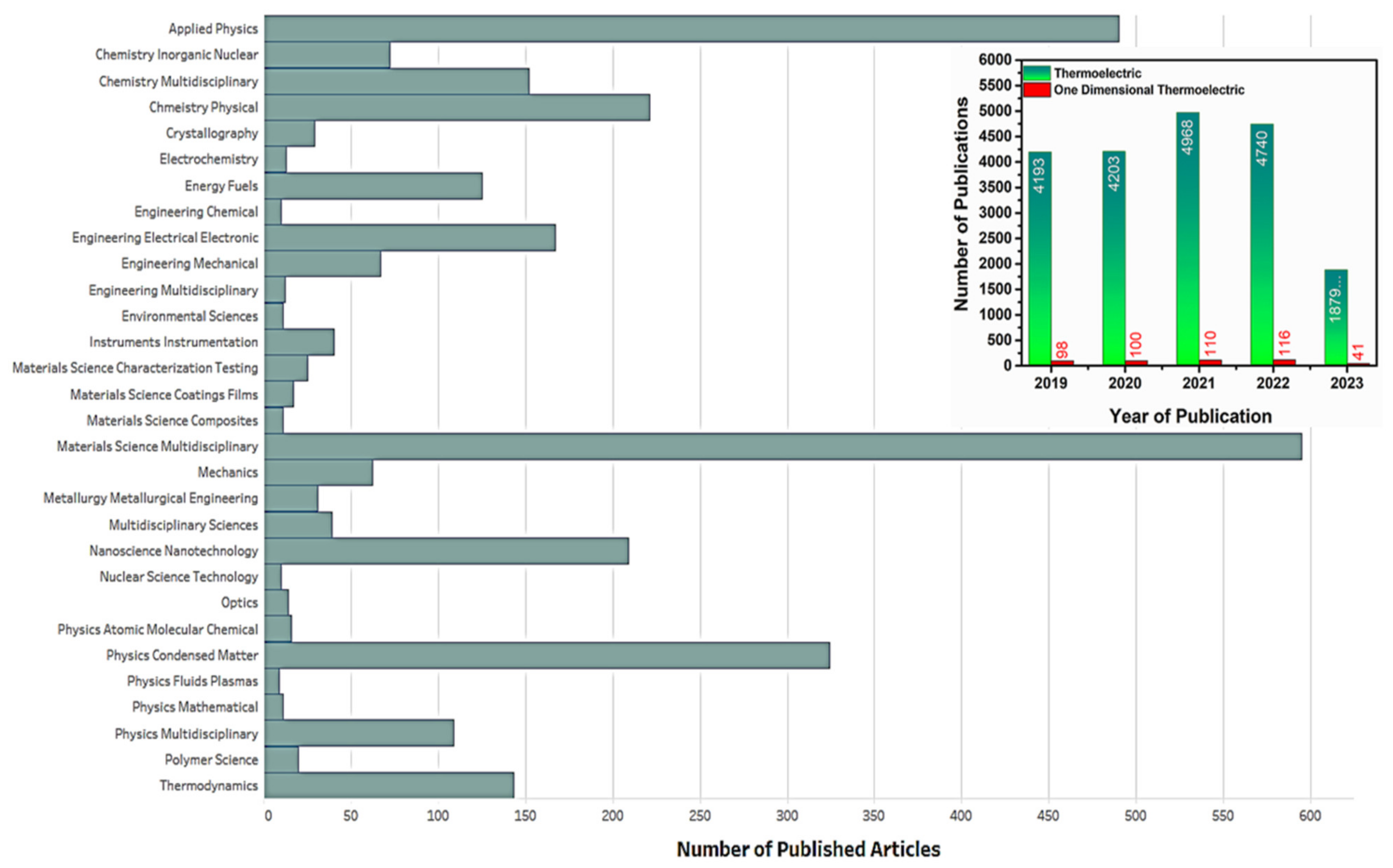
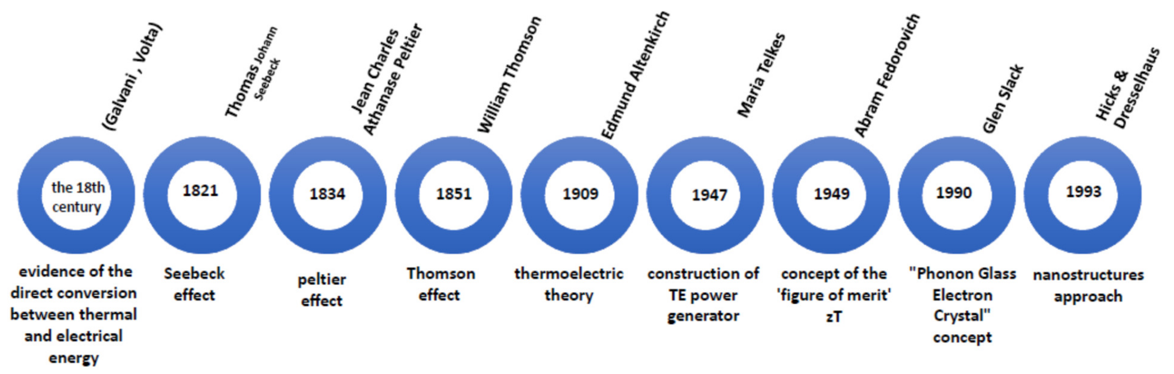
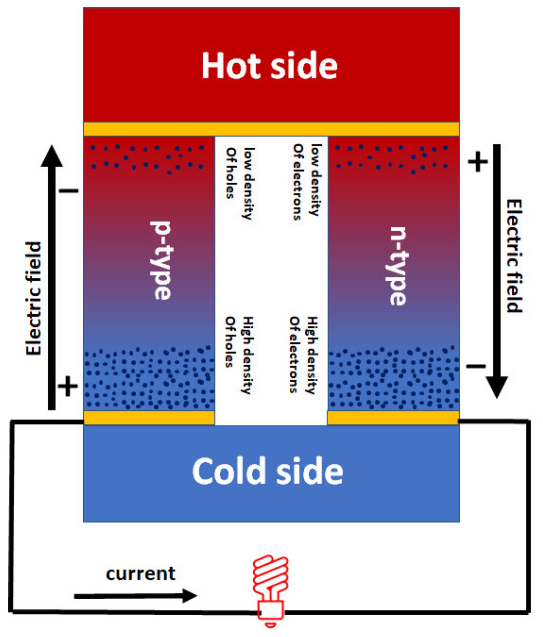
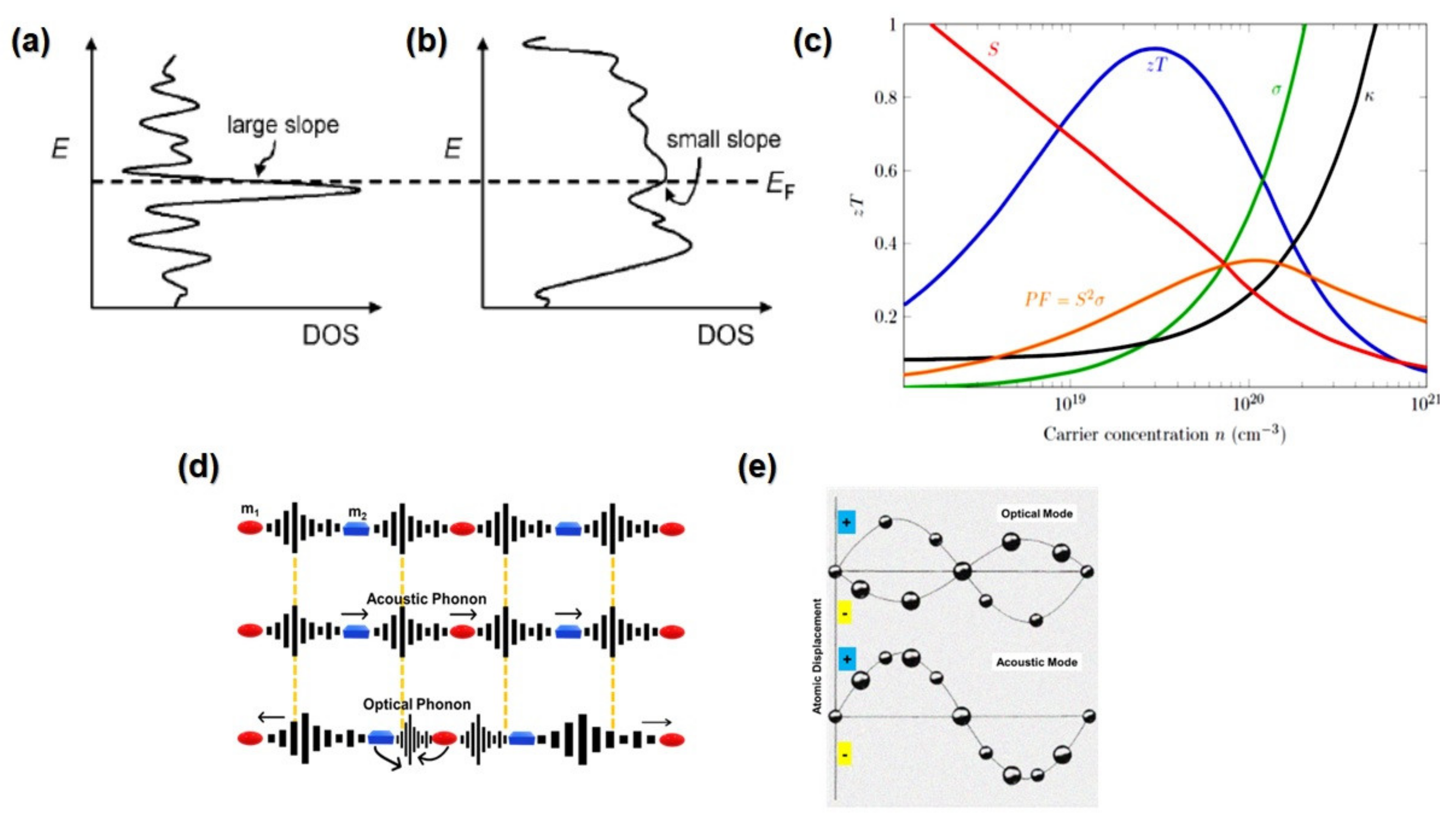
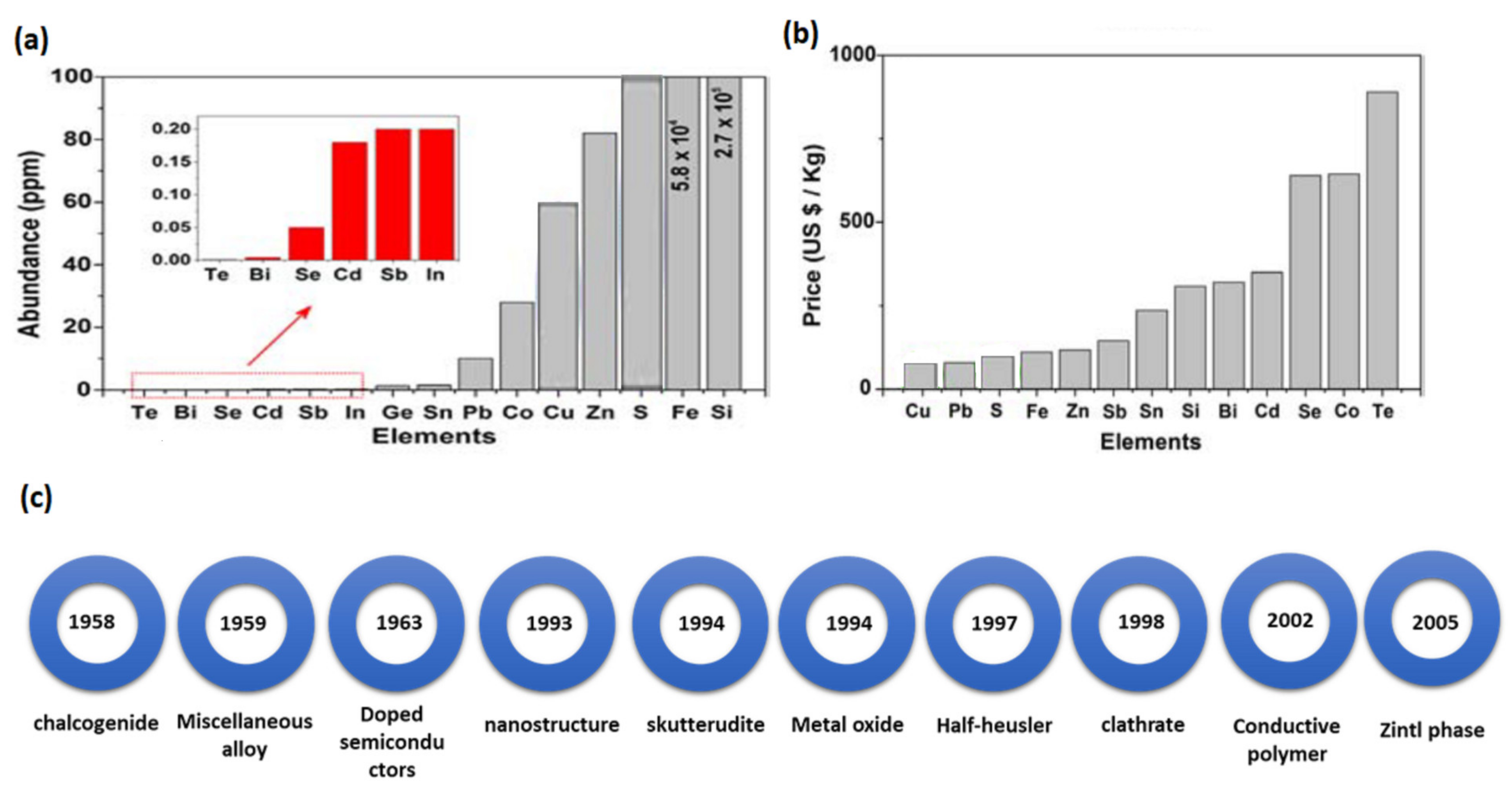
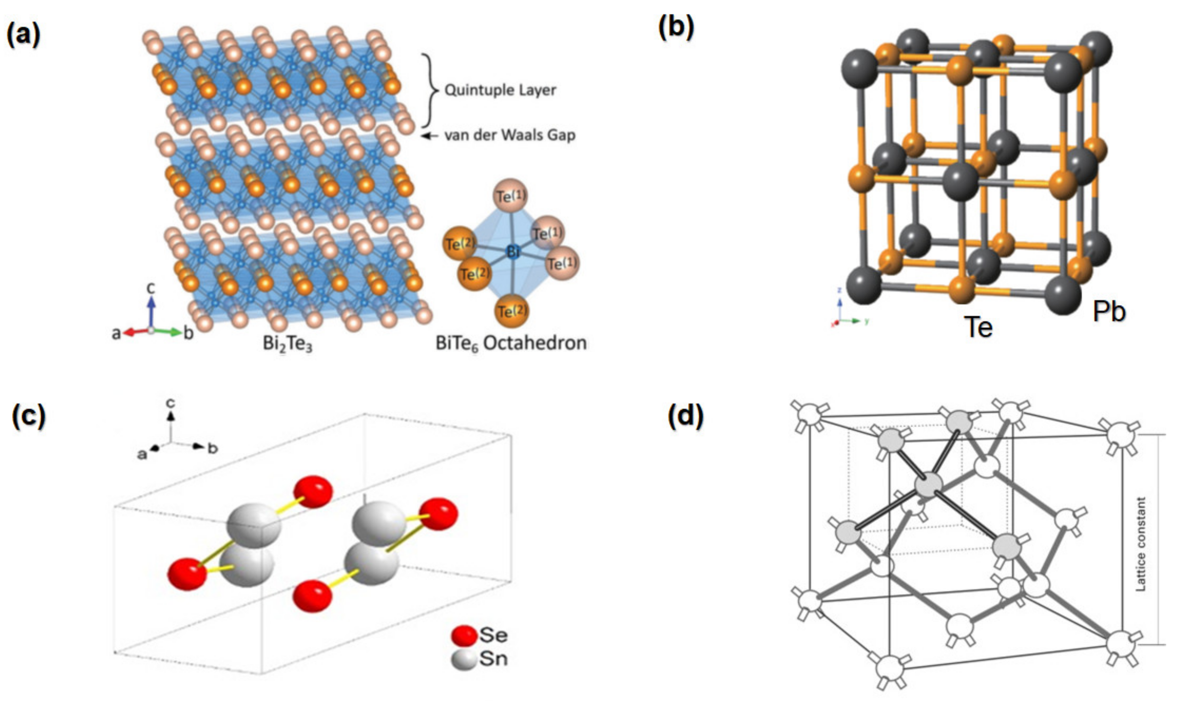
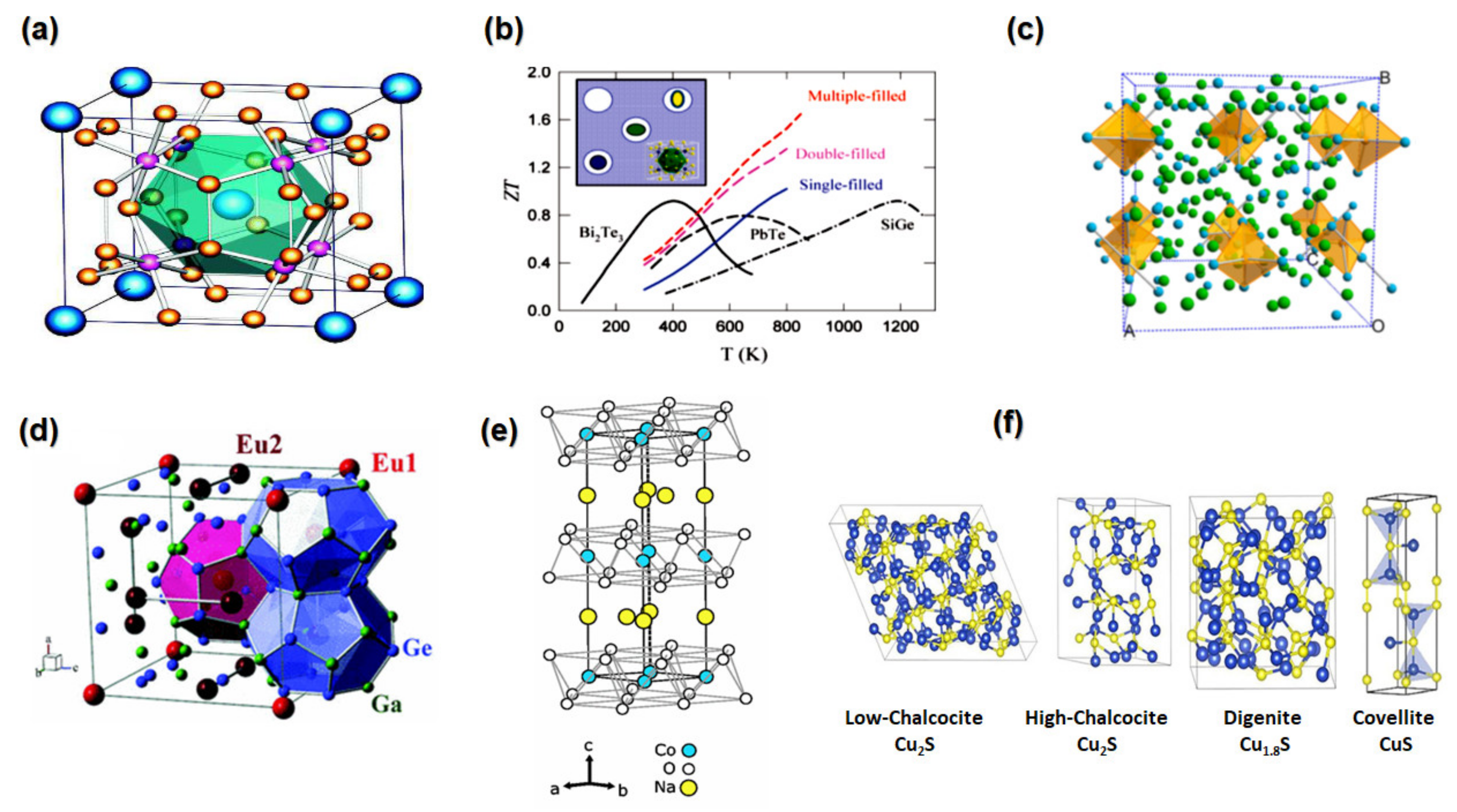
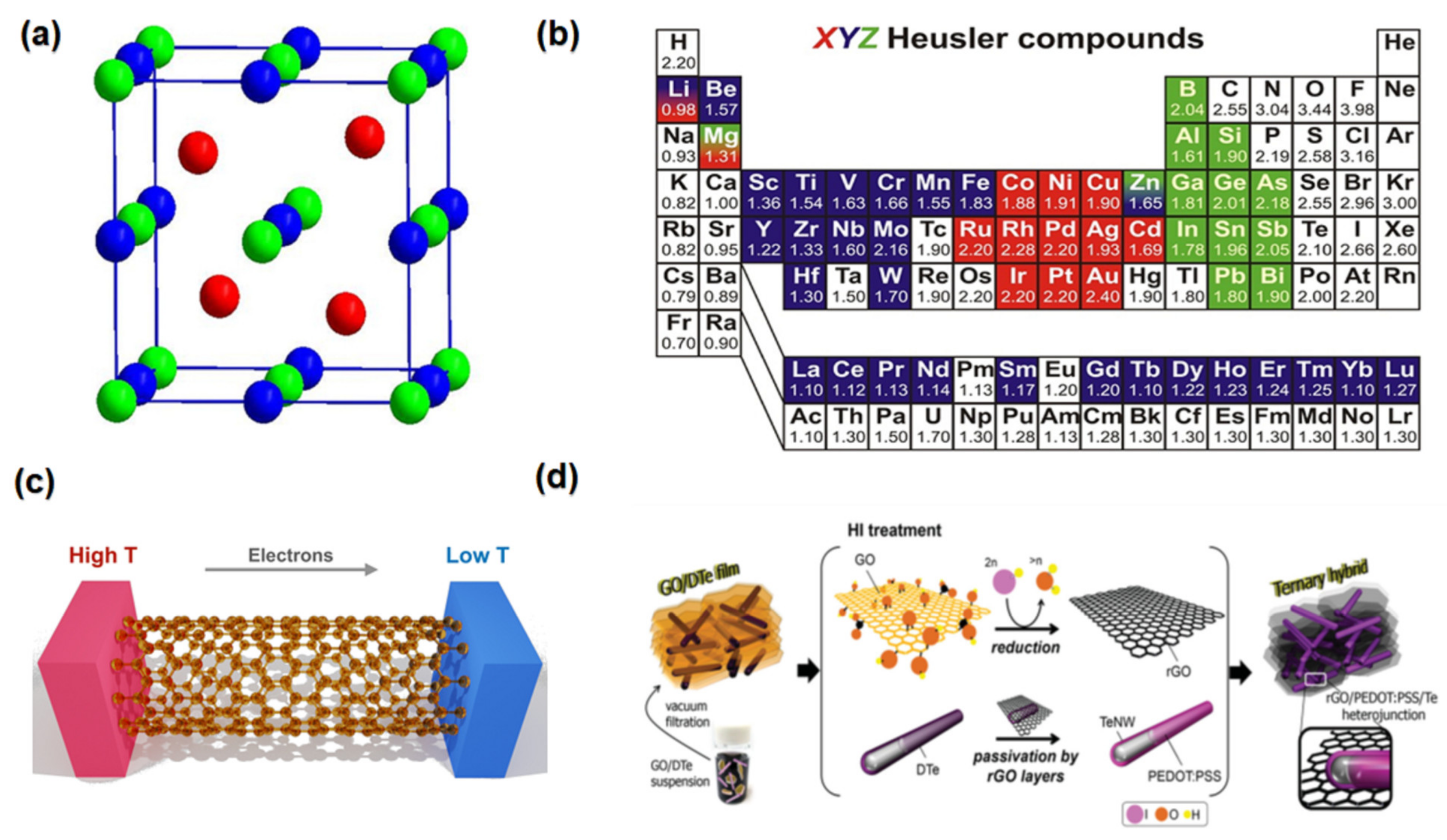
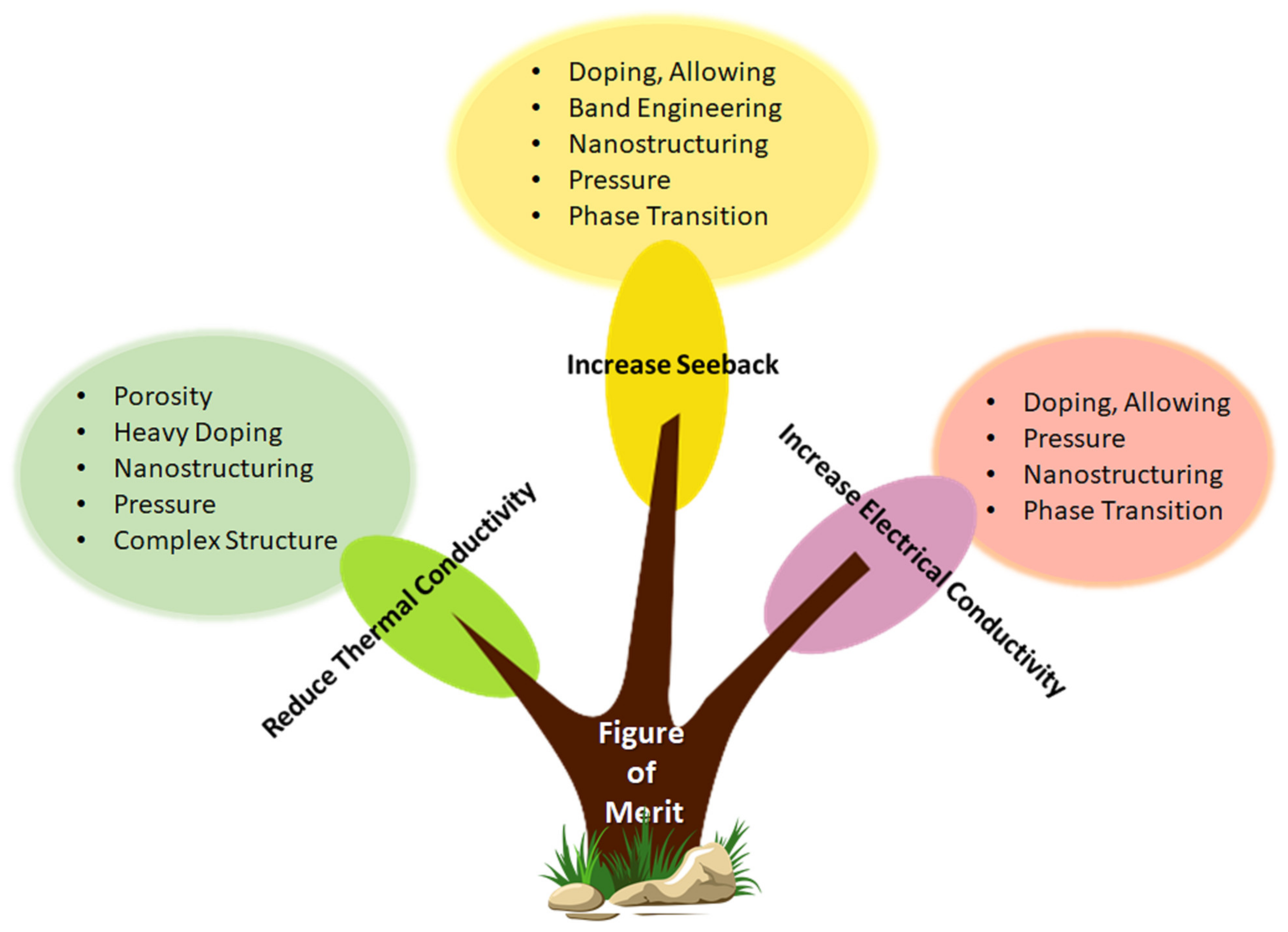
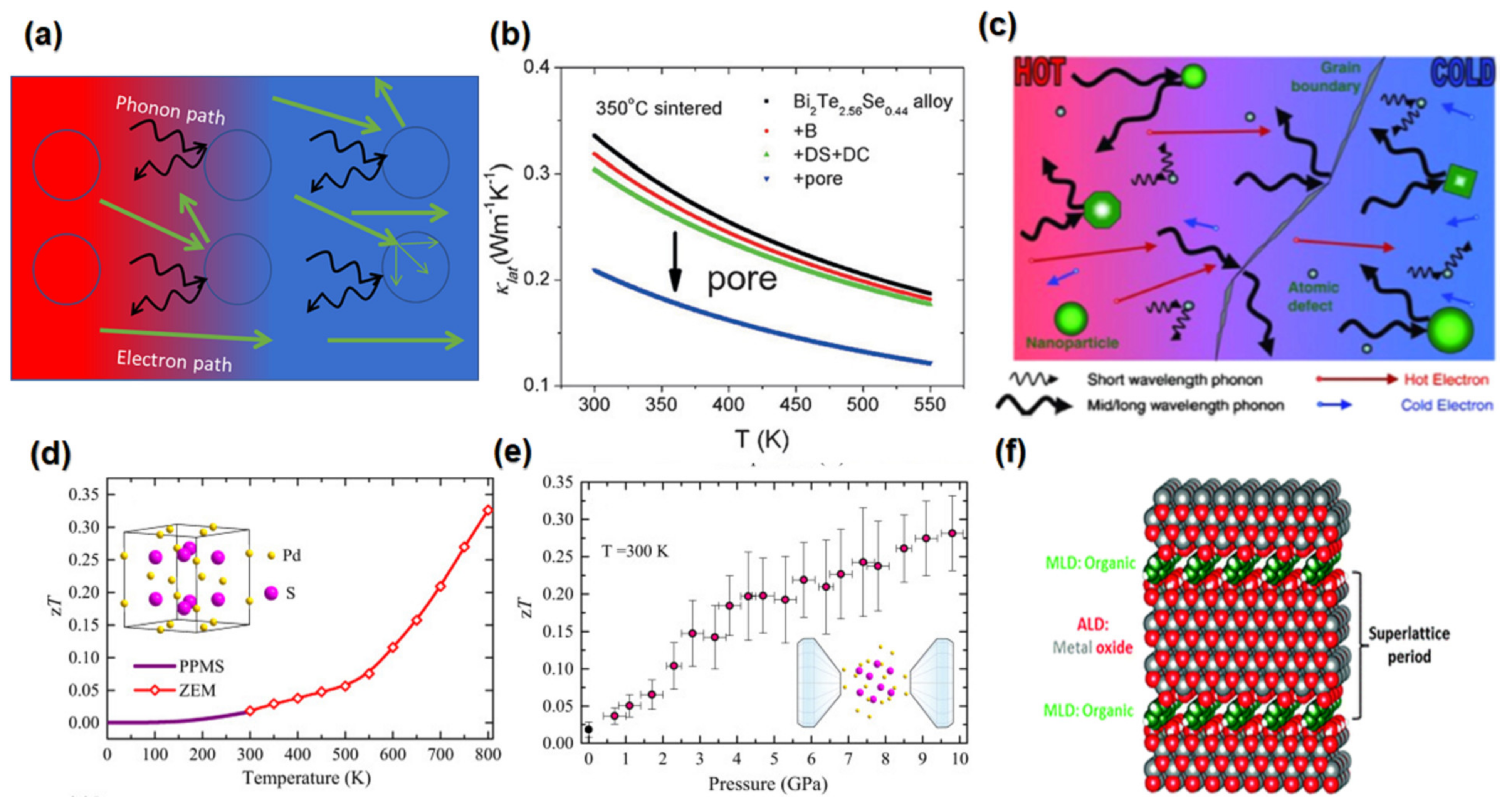
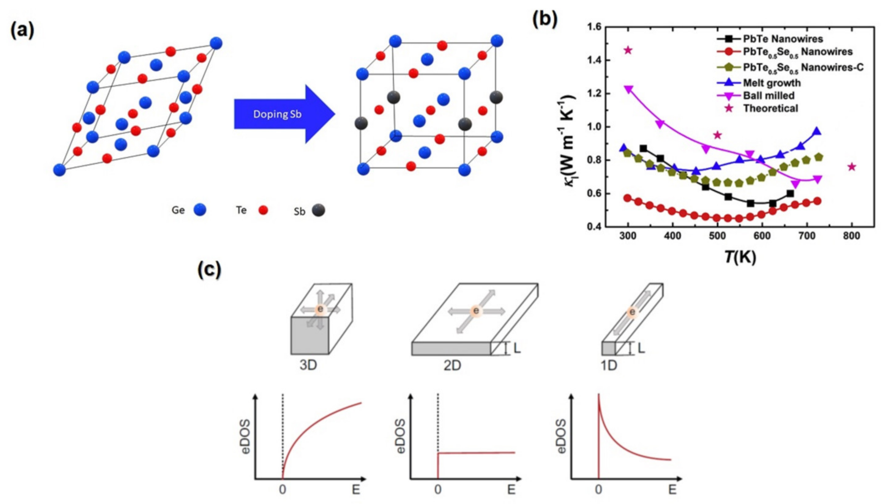
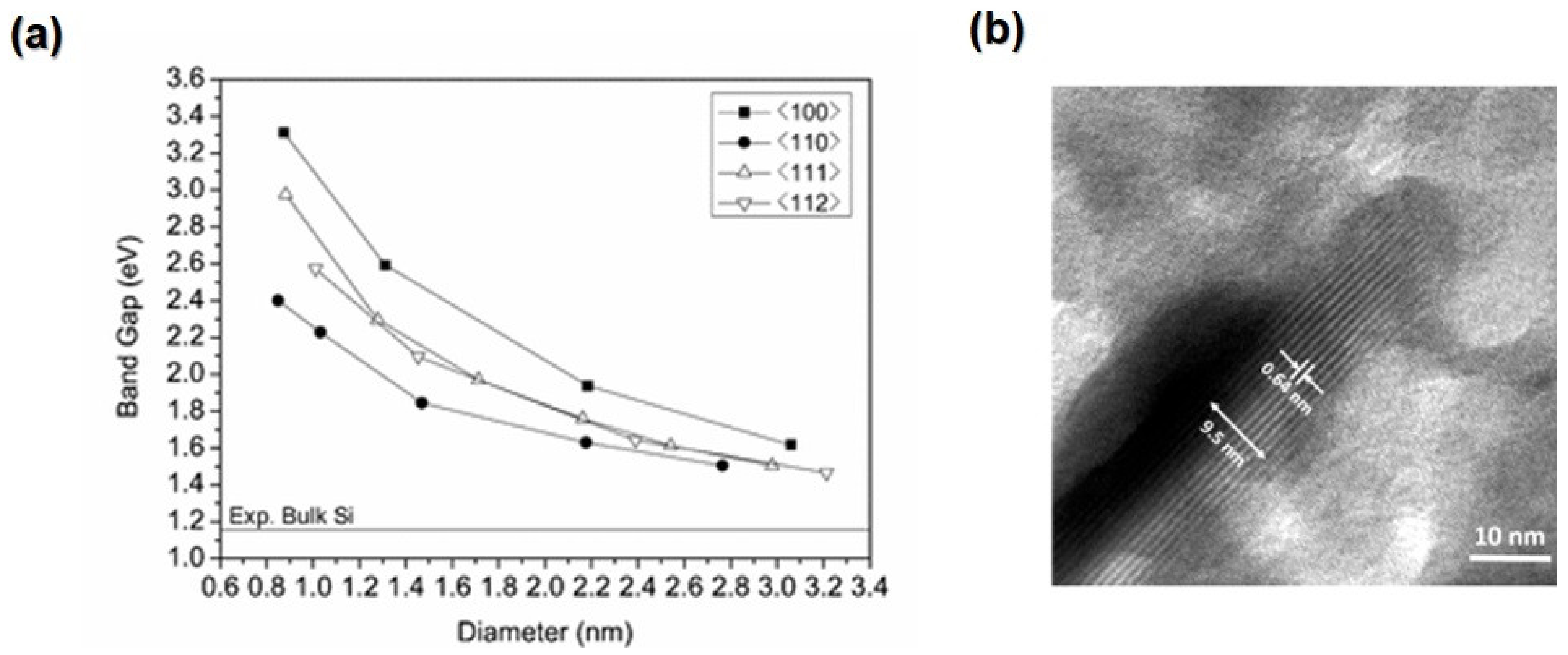
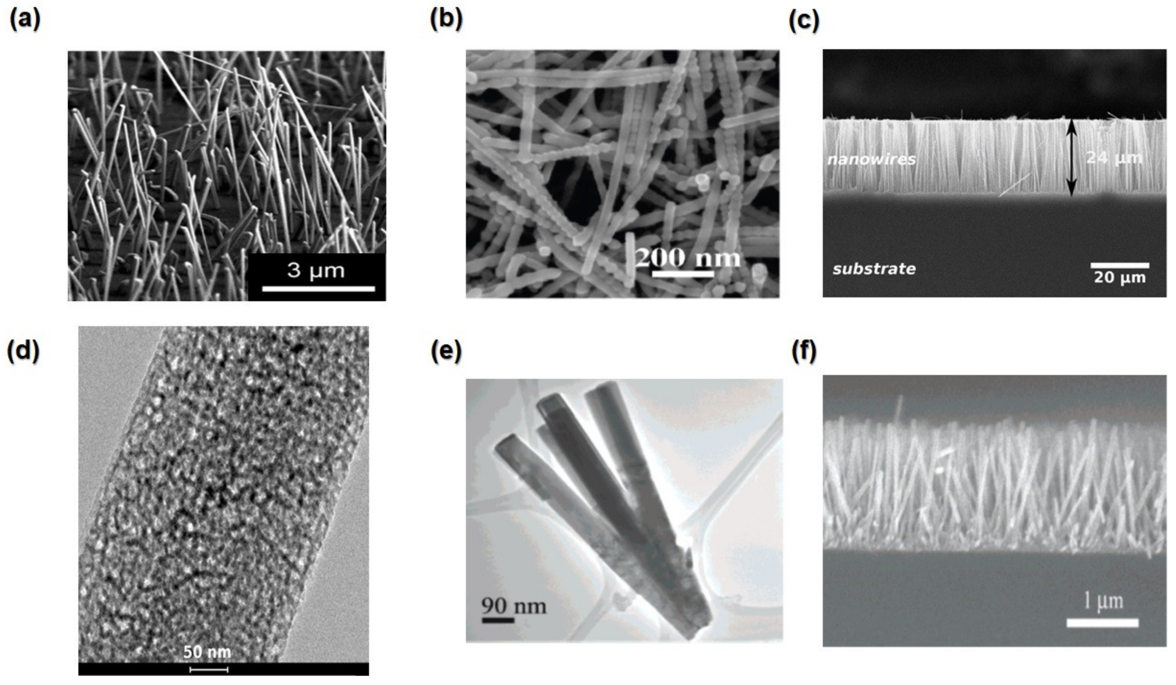
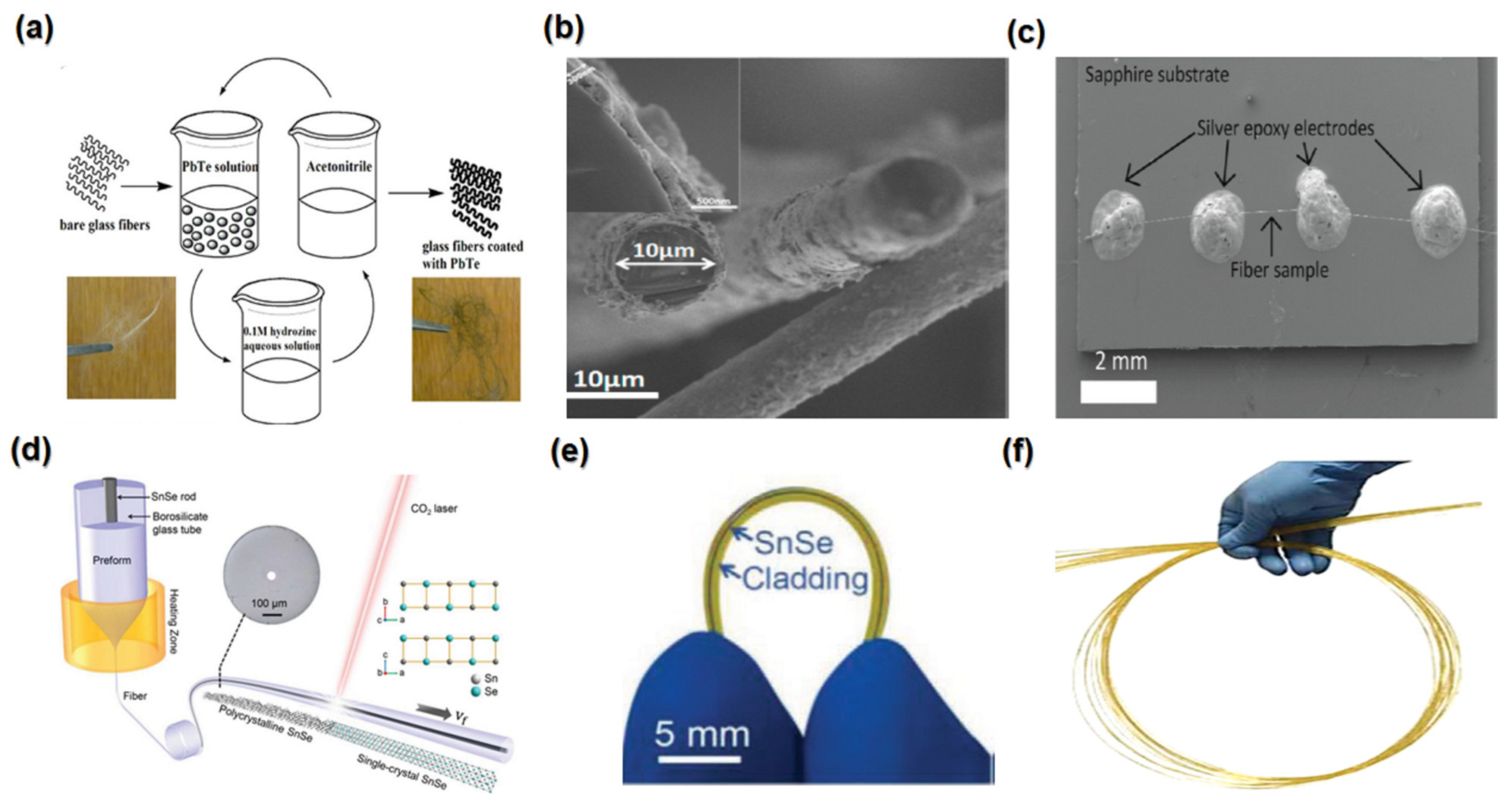
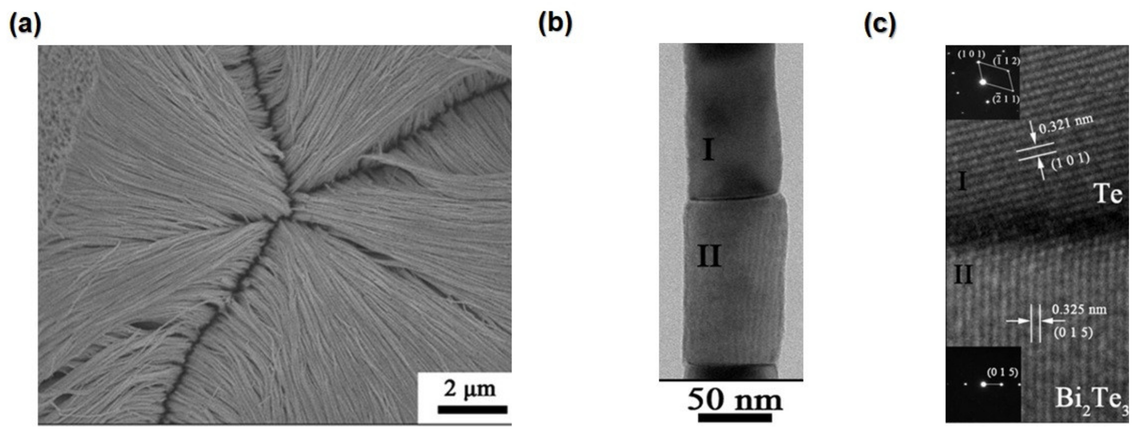
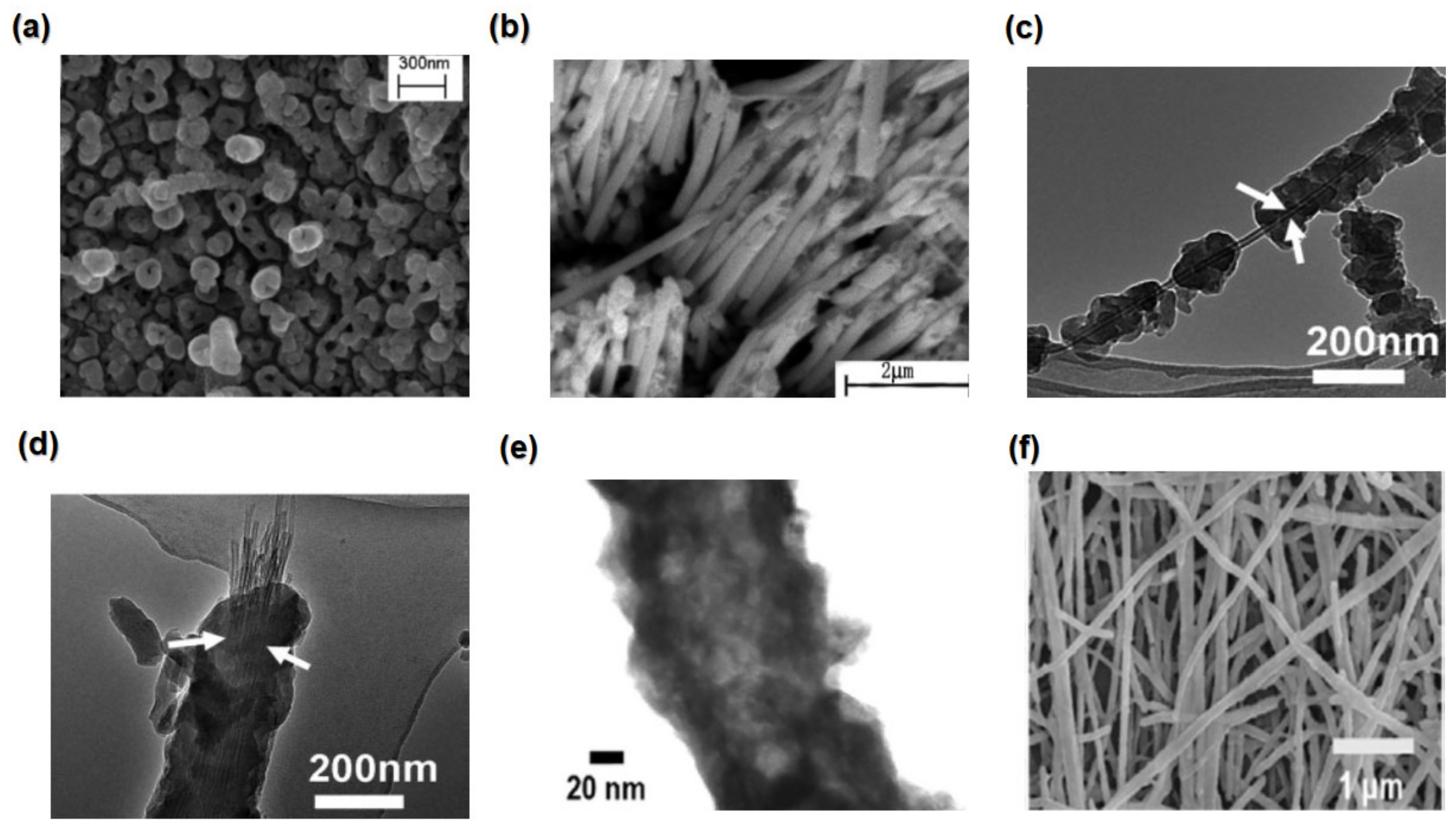
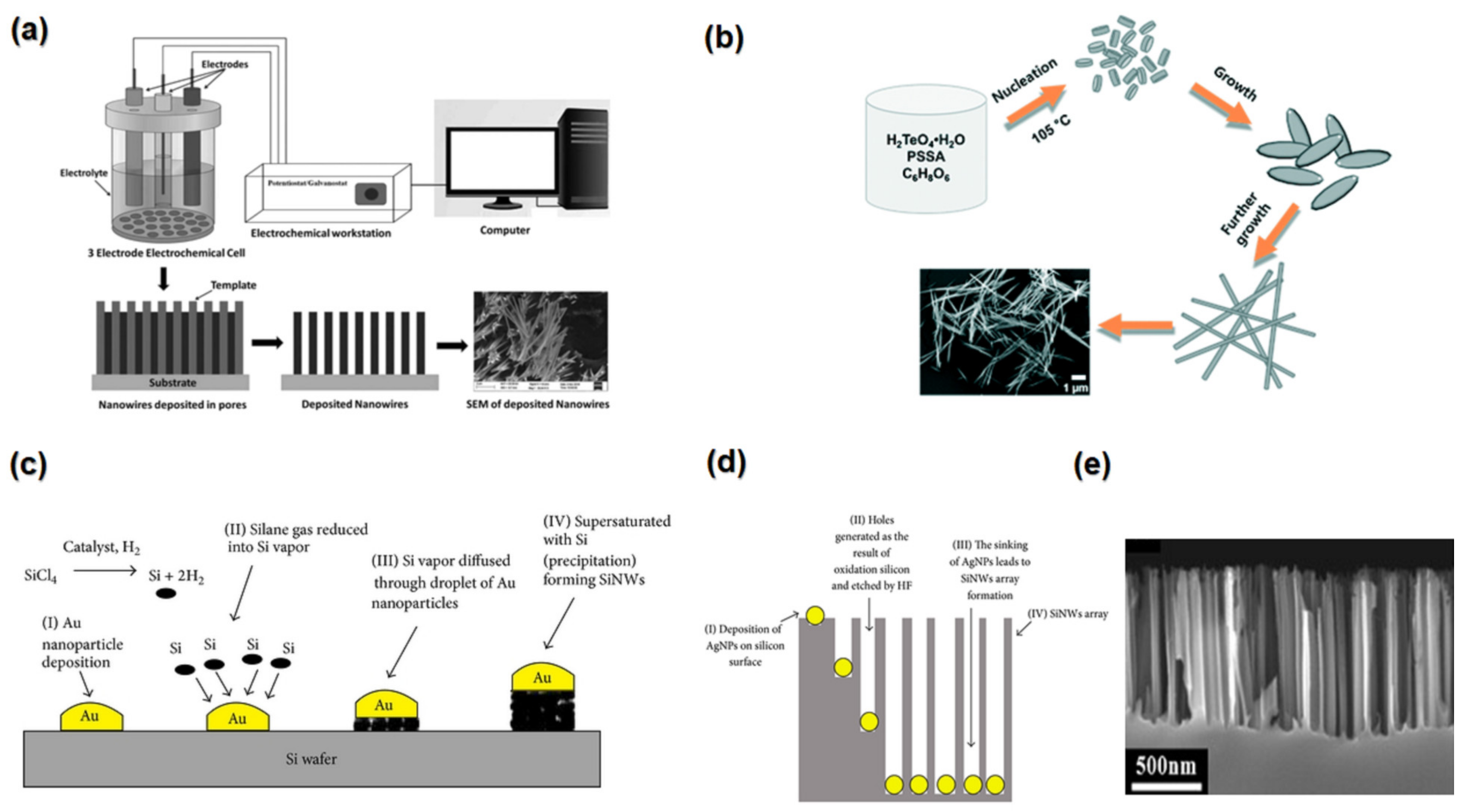
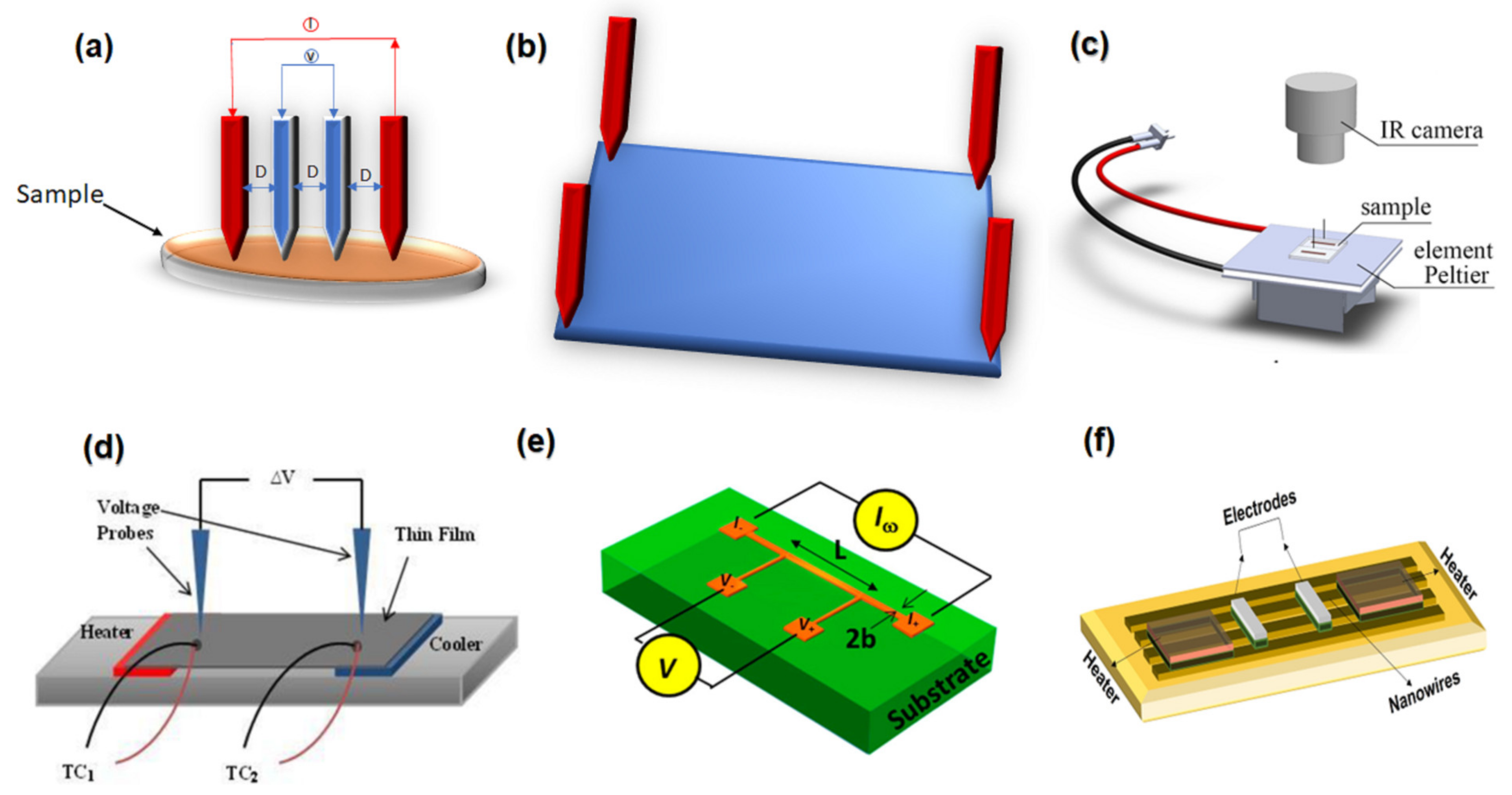
Figure 1. Comparison of publications on 1D TE and TE and application distribution across disciplines for 1D TE materials [15].
Nanomaterials 13 02011 g001
Figure 2. The key achievements in the evolution of the TE sector.
Nanomaterials 13 02011 g002
Figure 3. Schematic illustrating the working principle of TE materials.
Nanomaterials 13 02011 g003
Figure 4. The theoretical density of states (DOS) with (a) Large slope (b) Slight slope “Reproduced with permission from [36], WILEY-VCH, 2009”. (c) The effect of the carrier concentration on the Seebeck, electrical conductivity, thermal conductivity, TE power factor and ZT based on data from ref. [37]. (d) Acoustic and optical phonons in a 1D chain of atoms. Atoms with masses m1 (red) and m2 (blue) are arranged in an alternating configuration, while their displacements are represented by arrows [38]. (e) Different types of atomic displacement modes [39].
Nanomaterials 13 02011 g004
Figure 5. (a) The abundance of various elements on the earth’s crust. (b) Price of the common TE elements “Reproduced with permission from [49], WILEY-VCH, 2019”. (c) State of the art in TE materials discovery Cu and S (green) are the prevailing elements in terms of abundance and cost-effectiveness for the development of TE materials.
Nanomaterials 13 02011 g005
Figure 9. The most common methods for increasing the ZT value of thermoelements.
Nanomaterials 13 02011 g009
Table 1. Summaries the most well-known TE materials depend on their working temperature, their TE performance, and their properties.
NoState of Art MaterialMaterialConductivity TypeZTWorking Temperature
(K)
Seebeck Coefficient
(μVK−1)
Thermal Conductivity
(Wm−1K−1)
Electrical Conductivity
(S.cm−1)
StabilityToxic LevelCostRef.
1Bi2Te3Bi0.5Sb1.5Te3p-type1.863202420.65650 [165]
Te-embedded Bi2Te3n-type2.27375−2340.80825[166]
2Ternary CompositesSWNT/PANIp-type0.12300650.43769 [85]
CNTs/PEDOTn-type0.5300−12340.676.9[167]
3PbTePb0.98Na0.02Te–8%SrTep-type2.59233000.9250 [58]
PbTe0.996S0.001I0.003n-type1.7800−2251.25500[168]
4SnSeSnSep-type2.69233500.35100 [65]
SnSe0.97Br0.03n-type2.8773−4800.2541[169]
5PerovskiteLaCo0.92Ni0.08O2.9p-type0.23002200.3533.3 [170]
La-doped SrTiO3n-type0.271073−3003.180[111]
6SkutteruditesCe0.6Ni1.5Co2.5Sb12p-type0.45850 1531.62 600 [171]
Ba0.3In0.3Co4Sb12n-type1.4 850−1902.51300[172]
7Zintl PhaseYbCd1.85Mn0.15Sb2p-type1.146502500.4200 [173]
Mg3.15Mn0.05Sb1.5Bi0.49Te0.01n-type1.85723−3100.8220[174]
8clathratesBa8Au5.3Ge40.7p-type0.9680150150 [175]
Ba8Ni0.31Zn0.52Ga13.06Ge32.2n-type1.21000−2001.5400[102]
9Metal sulphidesCU1.97Sp-type1.710003000.5100 [123]
AgBiS2 n-type0.7820−3000.5120[176]
10Half-Heusler(Nb0.6Ta0.4)0.8Ti0.2p-type1.612002201.5550 [177]
Zr0.2Hf0.8NiSn0.985Sb0.015n-type1.11000−1905.51500[178]
11OxidesCa3Co4Op-type0.2910731554.4 (at room temp)151 [179]
ZnOn-type0.441000−3002100[114]
12Si-Ge alloysSi0.62Ge0.32Ni0.03B0.03p-type1.5610003211.47250 [180]
SiGe–Mg2Sin-type1.3950−3402.7240[79]
Green: favourable; Orange: neutral; Red: Unfavourable.
Table 2. Different types of 1d nanostructured configurations with their synthesis method and TE characterization.
1D Nanostructure ConfigurationSynthesis MethodDescriptionSeebeck Coefficient
(µV/K)
Electrical Conductivity
(S/cm)
Thermal Conductivity
(W/m·K)
Power Factor
(μW/K2.m)
ZTRef.
Quantum wires theoretically0.5 nm diameter of Bi2Te3 ----14[28]
EBD synthesis method 1D Te QWs formed locally in the aluminium oxide layer−800 at 300 K----[293]
Nanowires and nanorodsTheoreticallyBi NW----6 at 77 K[245]
Electrochemical
Deposition, AAO template
Bi0.5Sb1.5Te3 NWs with 67 nm diameter −150480-1080-[294]
Solution-grownBi2Te3 nanorods with 40 nm diameter −180----[295]
Nanofibers powder-processingBi0.5Sb1.5Te3 fibres−(207–268)153–189-0.3–0.4-[296]
Heterostructuresbench top solution methodBi2Te3/Sb2Te3 core-shell−110-0.4-0.4 at 480 K[297]
solution-phasePbTe/Bi2Te3 segments NWs achieve −3001100.5110001.2 at 600 K[298]
Nanotubeshydrothermal synthesisBi2Te3 nanotube--0.3--[285]
bottom-up synthesis and SPSAu-doped Bi2Te3 nanotube--0.4723000.95 at 480 K[299]
Disclaimer/Publisher’s Note: The statements, opinions and data contained in all publications are solely those of the individual author(s) and contributor(s) and not of MDPI and/or the editor(s). MDPI and/or the editor(s) disclaim responsibility for any injury to people or property resulting from any ideas, methods, instructions or products referred to in the content.

