

3D Magnonic Conduits by Direct Write Nanofabrication
 , , , , , , , and
Abstract
1. Introduction
2. Materials and Methods
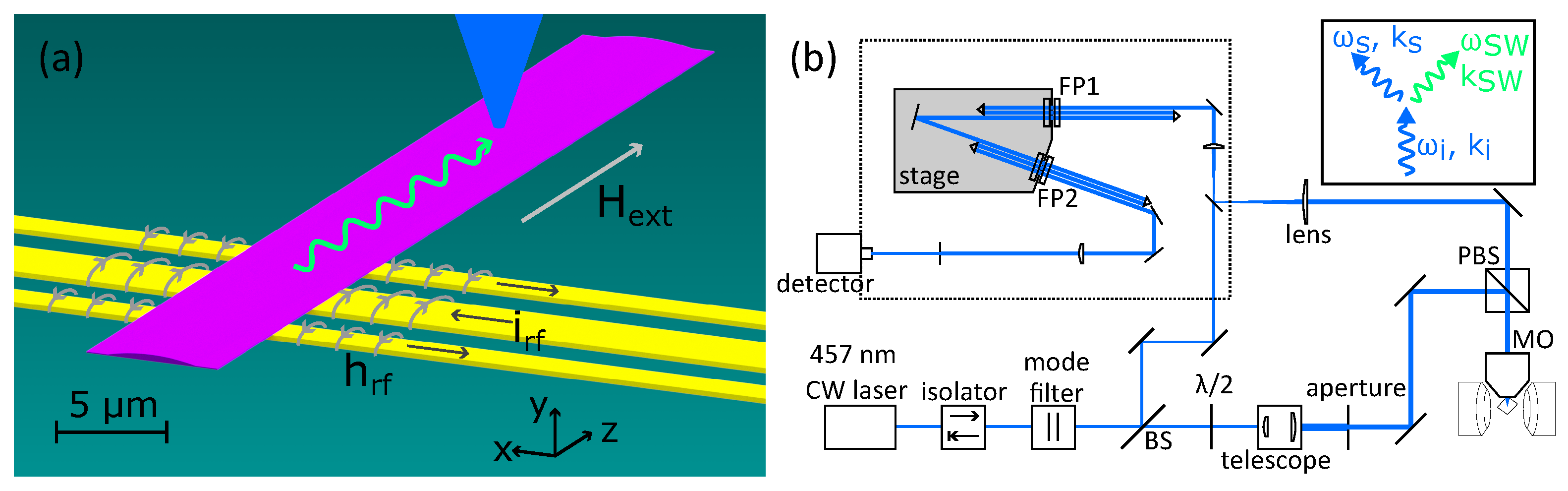
2.1. Fabrication
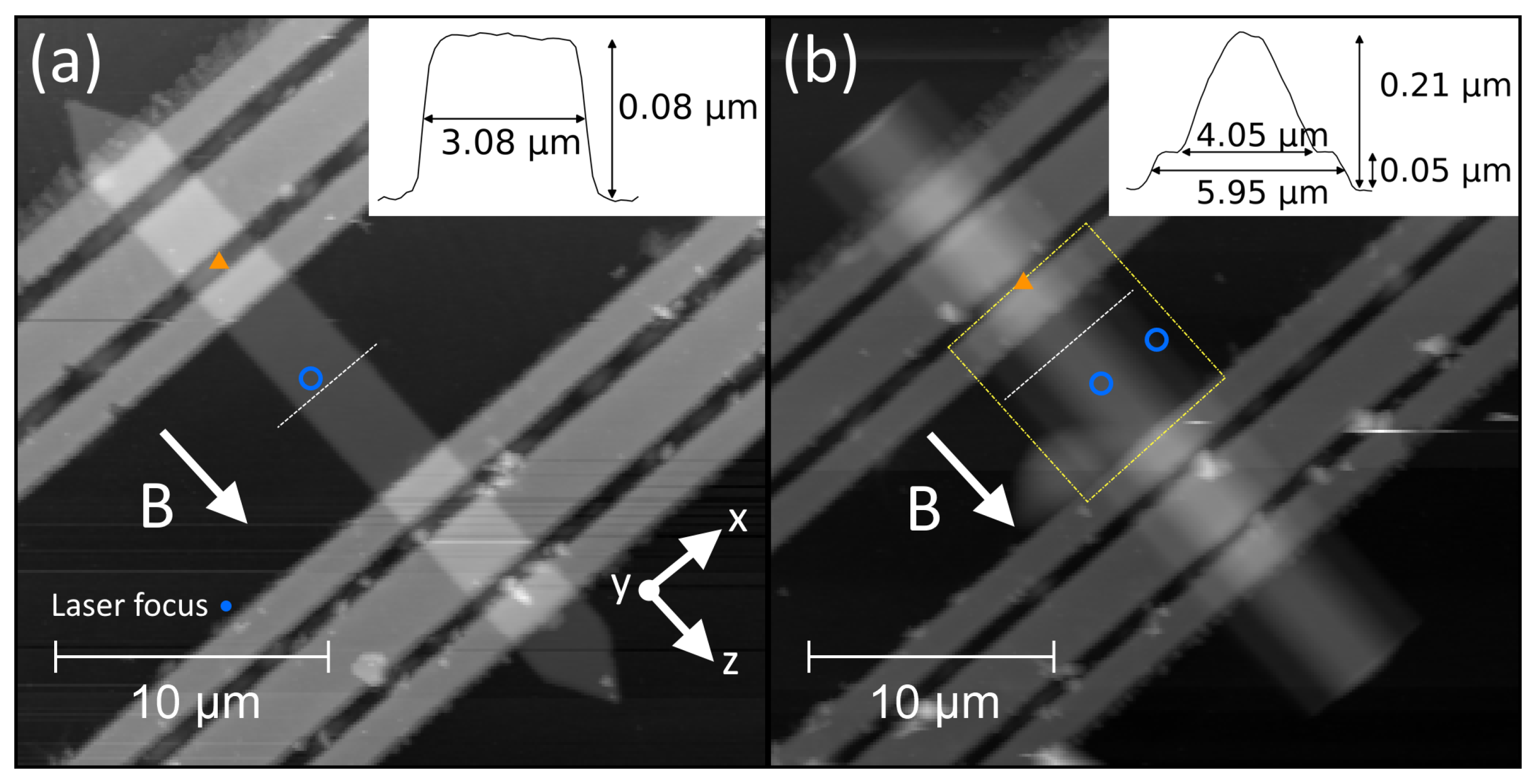
2.2. Characterisation
3. Results
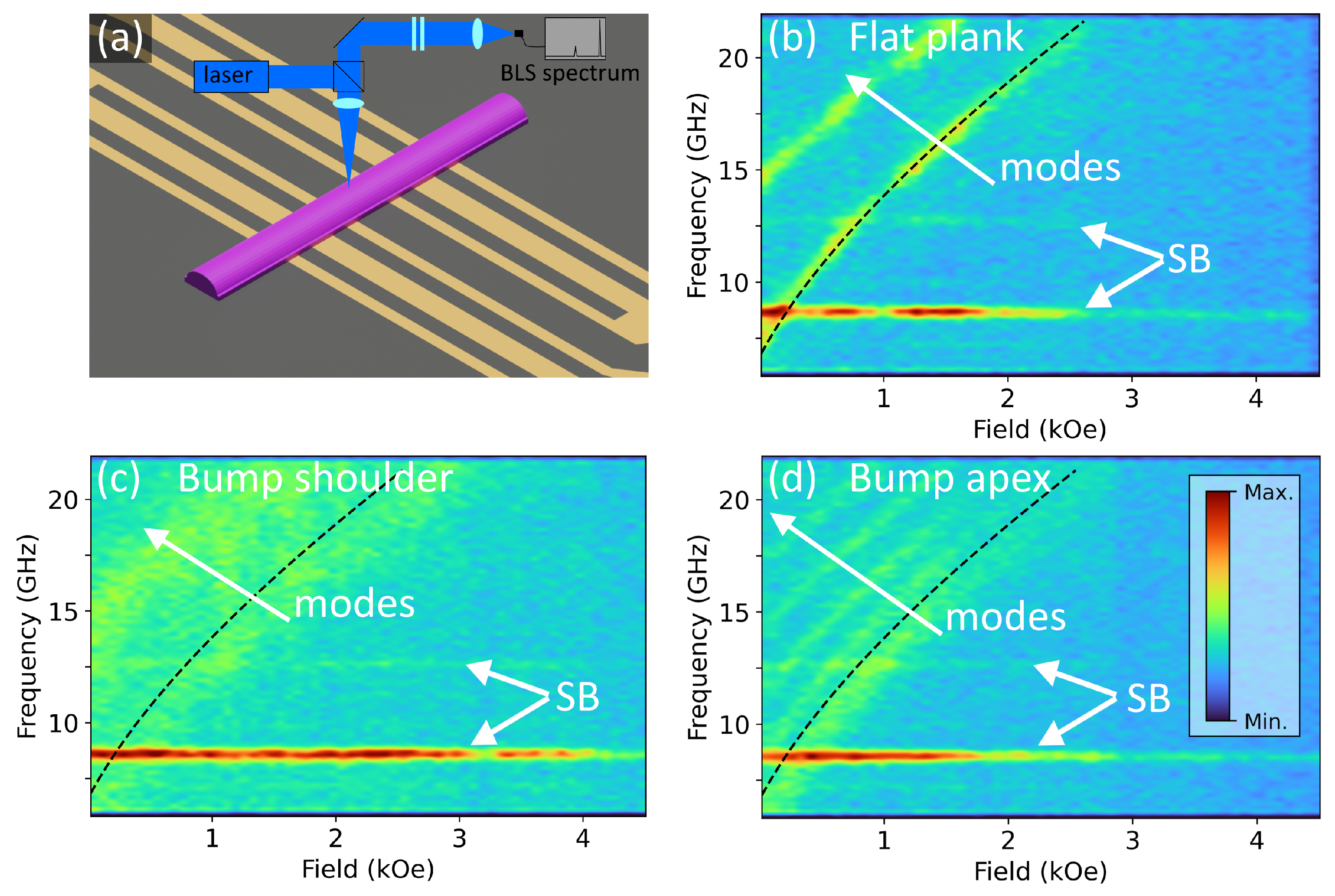
3.1. Thermal FMR
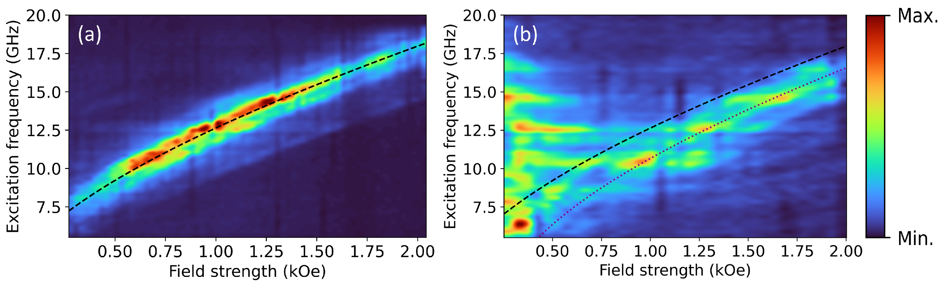
3.2. Microwave Excitation
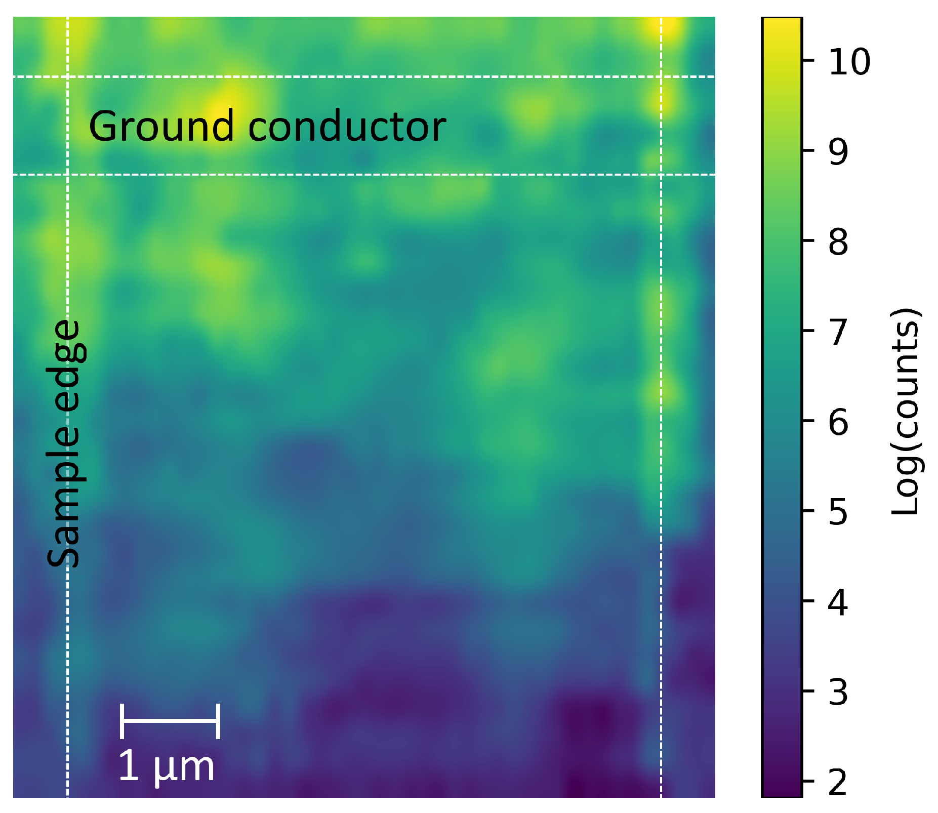
3.3. Area Scan
4. Discussion
5. Conclusions
Author Contributions
Funding
Data Availability Statement
Conflicts of Interest
References
- Barman, A.; Gubbiotti, G.; Ladak, S.; Adeyeye, A.O.; Krawczyk, M.; Grafe, J.; Adelmann, C.; Cotofana, S.; Naeemi, A.; Vasyuchka, V.I.; et al. The 2021 Magnonics Roadmap. J. Physics Condens. Matter 2021, 33, 413001. [Google Scholar] [CrossRef] [PubMed]
- Chumak, A.V.; Kabos, P.; Wu, M.; Abert, C.; Adelmann, C.; Adeyeye, A.O.; Akerman, J.; Aliev, F.G.; Anane, A.; Awad, A.; et al. Advances in Magnetics Roadmap on Spin-Wave Computing. IEEE Trans. Magn. 2022, 58, 3149664. [Google Scholar] [CrossRef]
- Wang, Q.; Kewenig, M.; Schneider, M.; Verba, R.; Kohl, F.; Heinz, B.; Geilen, M.; Mohseni, M.; Lägel, B.; Ciubotaru, F.; et al. A magnonic directional coupler for integrated magnonic half-adders. Nat. Electron. 2020, 3, 765–774. [Google Scholar] [CrossRef]
- Zakeri, K. Terahertz magnonics: Feasibility of using terahertz magnons for information processing. Phys. C Supercond. Appl. 2018, 549, 164–170. [Google Scholar] [CrossRef]
- Chumak, A.V.; Serga, A.A.; Hillebrands, B. Magnon transistor for all-magnon data processing. Nat. Commun. 2014, 5, 5700. [Google Scholar] [CrossRef] [PubMed]
- Dobrovolskiy, O.V.; Sachser, R.; Bunyaev, S.A.; Navas, D.; Bevz, V.M.; Zelent, M.; Śmigaj, W.; Rychły, J.; Krawczyk, M.; Vovk, R.V.; et al. Spin-Wave Phase Inverter upon a Single Nanodefect. ACS Appl. Mater. Interfaces 2019, 11, 17654–17662. [Google Scholar] [CrossRef] [PubMed]
- Fischer, T.; Kewenig, M.; Bozhko, D.A.; Serga, A.A.; Syvorotka, I.I.; Ciubotaru, F.; Adelmann, C.; Hillebrands, B.; Chumak, A.V. Experimental prototype of a spin-wave majority gate. Appl. Phys. Lett. 2017, 110, 152401. [Google Scholar] [CrossRef]
- Qin, H.; Holländer, R.B.; Flajšman, L.; Hermann, F.; Dreyer, R.; Woltersdorf, G.; van Dijken, S. Nanoscale magnonic Fabry-Pérot resonator for low-loss spin-wave manipulation. Nat. Commun. 2021, 12, 2293. [Google Scholar] [CrossRef]
- Yuan, H.Y.; Cao, Y.; Kamra, A.; Duine, R.A.; Yan, P. Quantum magnonics: When magnon spintronics meets quantum information science. Phys. Rep. 2022, 965, 1–74. [Google Scholar] [CrossRef]
- Mohseni, M.; Vasyuchka, V.I.; L’vov, V.S.; Serga, A.A.; Hillebrands, B. Classical analog of qubit logic based on a magnon Bose–Einstein condensate. Commun. Phys. 2022, 5, 196. [Google Scholar] [CrossRef]
- Andrianov, S.N.; Moiseev, S.A. Magnon qubit and quantum computing on magnon Bose–Einstein condensates. Phys. Rev. A At. Mol. Opt. Phys. 2014, 90, 042303. [Google Scholar] [CrossRef]
- Grollier, J.; Querlioz, D.; Camsari, K.Y.; Everschor-Sitte, K.; Fukami, S.; Stiles, M.D. Neuromorphic spintronics. Nat. Electron. 2020, 3, 360–370. [Google Scholar] [CrossRef] [PubMed]
- Demokritov, S.O.; Demidov, V.E.; Dzyapko, O.; Melkov, G.A.; Serga, A.A.; Hillebrands, B.; Slavin, A.N. Bose–Einstein condensation of quasi-equilibrium magnons at room temperature under pumping. Nature 2006, 443, 430–433. [Google Scholar] [CrossRef] [PubMed]
- Schneider, M.; Breitbach, D.; Serha, R.O.; Wang, Q.; Serga, A.A.; Slavin, A.N.; Tiberkevich, V.S.; Heinz, B.; Lägel, B.; Brächer, T.; et al. Control of the Bose–Einstein Condensation of Magnons by the Spin Hall Effect. Phys. Rev. Lett. 2021, 127, 237203. [Google Scholar] [CrossRef] [PubMed]
- Wang, Q.; Chumak, A.V.; Pirro, P. Inverse-design magnonic devices. Nat. Commun. 2021, 12, 2636. [Google Scholar] [CrossRef] [PubMed]
- Papp, A.; Porod, W.; Csaba, G. Nanoscale neural network using non-linear spin-wave interference. Nat. Commun. 2021, 12, 6422. [Google Scholar] [CrossRef] [PubMed]
- Vogel, M.; Chumak, A.V.; Waller, E.H.; Langner, T.; Vasyuchka, V.I.; Hillebrands, B.; Von Freymann, G. Optically reconfigurable magnetic materials. Nat. Phys. 2015, 11, 487–491. [Google Scholar] [CrossRef]
- Dobrovolskiy, O.V.; Sachser, R.; Brächer, T.; Böttcher, T.; Kruglyak, V.V.; Vovk, R.V.; Shklovskij, V.A.; Huth, M.; Hillebrands, B.; Chumak, A.V. Magnon–fluxon interaction in a ferromagnet/superconductor heterostructure. Nat. Phys. 2019, 15, 477–482. [Google Scholar] [CrossRef]
- Xu, M.; Yamamoto, K.; Puebla, J.; Baumgaertl, K.; Rana, B.; Miura, K.; Takahashi, H.; Grundler, D.; Maekawa, S.; Otani, Y. Nonreciprocal surface acoustic wave propagation via magneto-rotation coupling. Sci. Adv. 2020, 6, 1724. [Google Scholar] [CrossRef]
- Papp, A.; Kiechle, M.; Mendisch, S.; Ahrens, V.; Sahin, L.; Seitner, L.; Porod, W.; Csaba, G.; Becherer, M. Experimental demonstration of a concave grating for spin waves in the Rowland arrangement. Sci. Rep. 2021, 11, 14239. [Google Scholar] [CrossRef]
- Dobrovolskiy, O.V.; Vovk, N.R.; Bondarenko, A.V.; Bunyaev, S.A.; Lamb-Camarena, S.; Zenbaa, N.; Sachser, R.; Barth, S.; Guslienko, K.Y.; Chumak, A.V.; et al. Spin-wave eigenmodes in direct-write 3D nanovolcanoes. Appl. Phys. Lett. 2021, 118, 132405. [Google Scholar] [CrossRef]
- Körber, L.; Zimmermann, M.; Wintz, S.; Finizio, S.; Kronseder, M.; Bougeard, D.; Dirnberger, F.; Weigand, M.; Raabe, J.; Otálora, J.A.; et al. Symmetry and curvature effects on spin waves in vortex-state hexagonal nanotubes. Phys. Rev. B 2021, 104, 184429. [Google Scholar] [CrossRef]
- Li, X.; Labanowski, D.; Salahuddin, S.; Lynch, C.S. Spin wave generation by surface acoustic waves. J. Appl. Phys. 2017, 122, 043904. [Google Scholar] [CrossRef]
- Heinz, B.; Brächer, T.; Schneider, M.; Wang, Q.; Lägel, B.; Friedel, A.M.; Breitbach, D.; Steinert, S.; Meyer, T.; Kewenig, M.; et al. Propagation of Spin-Wave Packets in Individual Nanosized Yttrium Iron Garnet Magnonic Conduits. Nano Lett. 2020, 20, 4220–4227. [Google Scholar] [CrossRef] [PubMed]
- Wang, Q.; Heinz, B.; Verba, R.; Kewenig, M.; Pirro, P.; Schneider, M.; Meyer, T.; Lägel, B.; Dubs, C.; Brächer, T.; et al. Spin Pinning and Spin-Wave Dispersion in Nanoscopic Ferromagnetic Waveguides. Phys. Rev. Lett. 2019, 122, 247202. [Google Scholar] [CrossRef] [PubMed]
- Gubbiotti, G. (Ed.) Three-Dimensional Magnonics; Jenny Stanford Publishing: New York, NY, USA, 2019. [Google Scholar] [CrossRef]
- Garlando, U.; Wang, Q.; Dobrovolskiy, O.V.; Chumak, A.V.; Riente, F. Numerical Model for 32-bit Magnonic Ripple Carry Adder. arXiv 2023, arXiv:2109.12973. [Google Scholar] [CrossRef]
- May, A.; Saccone, M.; van den Berg, A.; Askey, J.; Hunt, M.; Ladak, S. Magnetic charge propagation upon a 3D artificial spin-ice. Nat. Commun. 2021, 12, 3217. [Google Scholar] [CrossRef] [PubMed]
- Ho, P.; Tan, A.K.; Goolaup, S.; Oyarce, A.L.; Raju, M.; Huang, L.S.; Soumyanarayanan, A.; Panagopoulos, C. Geometrically tailored skyrmions at zero magnetic field in multilayered nanostructures. Phys. Rev. Appl. 2019, 11, 024064. [Google Scholar] [CrossRef]
- Sheka, D.D. A perspective on curvilinear magnetism. Appl. Phys. Lett. 2021, 118, 230502. [Google Scholar] [CrossRef]
- Makarov, D.; Volkov, O.M.; Kákay, A.; Pylypovskyi, O.V.; Budinská, B.; Dobrovolskiy, O.V.; Makarov, D.; Volkov, O.M.; Kákay, A.; Pylypovskyi, O.V.; et al. New Dimension in Magnetism and Superconductivity: 3D and Curvilinear Nanoarchitectures. Adv. Mater. 2022, 34, 2101758. [Google Scholar] [CrossRef] [PubMed]
- Fernández-Pacheco, A.; Streubel, R.; Fruchart, O.; Hertel, R.; Fischer, P.; Cowburn, R.P. Three-dimensional nanomagnetism. Nat. Commun. 2017, 8, 15756. [Google Scholar] [CrossRef] [PubMed]
- Smith, E.J.; Makarov, D.; Sanchez, S.; Fomin, V.M.; Schmidt, O.G. Magnetic microhelix coil structures. Phys. Rev. Lett. 2011, 107, 097204. [Google Scholar] [CrossRef] [PubMed]
- Sanz-Hernández, D.; Hamans, R.F.; Osterrieth, J.; Liao, J.W.; Skoric, L.; Fowlkes, J.D.; Rack, P.D.; Lippert, A.; Lee, S.F.; Lavrijsen, R.; et al. Fabrication of Scaffold-Based 3D Magnetic Nanowires for Domain Wall Applications. Nanomaterials 2018, 8, 483. [Google Scholar] [CrossRef] [PubMed]
- Harinarayana, V.; Shin, Y.C. Two-photon lithography for three-dimensional fabrication in micro/nanoscale regime: A comprehensive review. Opt. Laser Technol. 2021, 142, 107180. [Google Scholar] [CrossRef]
- Fernández-Pacheco, A.; Skoric, L.; De Teresa, J.M.; Pablo-Navarro, J.; Huth, M.; Dobrovolskiy, O.V. Writing 3D Nanomagnets Using Focused Electron Beams. Materials 2020, 13, 3774. [Google Scholar] [CrossRef] [PubMed]
- Höflich, K.; Hobler, G.; Allen, F.I.; Wirtz, T.; Rius, G.; Krasheninnikov, A.V.; Schmidt, M.; Utke, I.; Klingner, N.; Osenberg, M. Roadmap for focused ion beam technologies. arXiv 2023, arXiv:2305.19631. [Google Scholar]
- Weitzer, A.; Huth, M.; Kothleitner, G.; Plank, H. Expanding FEBID-Based 3D-Nanoprinting toward Closed High-Fidelity Nanoarchitectures. ACS Appl. Electron. Mater. 2022, 4, 744–754. [Google Scholar] [CrossRef]
- Córdoba, R.; Orús, P.; Strohauer, S.; Torres, T.E.; De Teresa, J.M. Ultra-fast direct growth of metallic micro- and nano-structures by focused ion beam irradiation. Sci. Rep. X 2019, 9, 14076. [Google Scholar] [CrossRef]
- Dobrovolskiy, O.V.; Begun, E.; Bevz, V.M.; Sachser, R.; Huth, M. Upper Frequency Limits for Vortex Guiding and Ratchet Effects. Phys. Rev. Appl. 2020, 13, 024012. [Google Scholar] [CrossRef]
- Heil, T.; Waldow, M.; Capelli, R.; Schneider, H.; Ahmels, L.; Tu, F.; Schoneberg, J.; Marbach, H. Pushing the limits of EUV mask repair: Addressing sub-10 nm defects with the next generation e-beam-based mask repair tool. J. Micro/Nanopatterning Mater. Metrol. 2021, 20, 031013. [Google Scholar] [CrossRef]
- Bunyaev, S.A.; Budinska, B.; Sachser, R.; Wang, Q.; Levchenko, K.; Knauer, S.; Bondarenko, A.V.; Urbánek, M.; Guslienko, K.Y.; Chumak, A.V.; et al. Engineered magnetization and exchange stiffness in direct-write Co–Fe nanoelements. Appl. Phys. Lett. 2021, 118, 022408. [Google Scholar] [CrossRef]
- Urbánek, M.; Flajšman, L.; Křiáková, V.; Gloss, J.; Horký, M.; Schmid, M.; Varga, P. Research Update: Focused ion beam direct writing of magnetic patterns with controlled structural and magnetic properties. APL Mater. 2018, 6, 060701. [Google Scholar] [CrossRef]
- Davies, C.S.; Francis, A.; Sadovnikov, A.V.; Chertopalov, S.V.; Bryan, M.T.; Grishin, S.V.; Allwood, D.A.; Sharaevskii, Y.P.; Nikitov, S.A.; Kruglyak, V.V. Towards graded-index magnonics: Steering spin waves in magnonic networks. Phys. Rev. B Condens. Matter Mater. Phys. 2015, 92, 020408. [Google Scholar] [CrossRef]
- Gruszecki, P.; Krawczyk, M. Spin-wave beam propagation in ferromagnetic thin films with graded refractive index: Mirage effect and prospective applications. Phys. Rev. B 2018, 97, 094424. [Google Scholar] [CrossRef]
- Kiechle, M.; Papp, A.; Mendisch, S.; Ahrens, V.; Golibrzuch, M.; Bernstein, G.H.; Porod, W.; Csaba, G.; Becherer, M.; Kiechle, M.; et al. Spin-Wave Optics in YIG Realized by Ion-Beam Irradiation. Small 2023, 19, e2207293. [Google Scholar] [CrossRef]
- Lara, A.; Dobrovolskiy, O.V.; Prieto, J.L.; Huth, M.; Aliev, F.G. Magnetization reversal assisted by half antivortex states in nanostructured circular cobalt disks. Appl. Phys. Lett. 2014, 105, 182402. [Google Scholar] [CrossRef]
- Khitun, A.; Bao, M.; Wang, K.L. Magnonic logic circuits. J. Phys. D Appl. Phys. 2010, 43, 264005. [Google Scholar] [CrossRef]
- Vaňatka, M.; Szulc, K.; Wojewoda, O.; Dubs, C.; Chumak, A.V.; Krawczyk, M.; Dobrovolskiy, O.V.; Kłos, J.W.; Urbánek, M. Spin-Wave Dispersion Measurement by Variable-Gap Propagating Spin-Wave Spectroscopy. Phys. Rev. Appl. 2021, 16, 54033. [Google Scholar] [CrossRef]
- Porrati, F.; Pohlit, M.; Müller, J.; Barth, S.; Biegger, F.; Gspan, C.; Plank, H.; Huth, M. Direct writing of CoFe alloy nanostructures by focused electron beam induced deposition from a heteronuclear precursor. Nanotechnology 2015, 26, 475701. [Google Scholar] [CrossRef] [PubMed]
- Sebastian, T.; Schultheiss, K.; Obry, B.; Hillebrands, B.; Schultheiss, H. Micro-focused Brillouin light scattering: Imaging spin waves at the nanoscale. Front. Phys. 2015, 3, 35. [Google Scholar] [CrossRef]
- Kakazel, G.N.; Wigen, P.E.; Guslienko, K.Y.; Chantrell, R.W.; Lesnik, N.A.; Metlushko, V.; Shima, H.; Fukamichi, K.; Otani, Y.; Novosad, V. In-plane and out-of-plane uniaxial anisotropies in rectangular arrays of circular dots studied by ferromagnetic resonance. J. Appl. Phys. 2003, 93, 8418–8420. [Google Scholar] [CrossRef]
- Lendinez, S.; Taghipour Kaffash, M.; Jungfleisch, M.B. Observation of mode splitting in artificial spin ice: A comparative ferromagnetic resonance and Brillouin light scattering study. Appl. Phys. Lett. 2021, 118, 162407. [Google Scholar] [CrossRef]
- Kittel, C. Excitation of Spin Waves in a Ferromagnet by a Uniform rf Field. Phys. Rev. 1958, 110, 1295. [Google Scholar] [CrossRef]
- Kalarickal, S.S.; Krivosik, P.; Wu, M.; Patton, C.E.; Schneider, M.L.; Kabos, P.; Silva, T.J.; Nibarger, J.P. Ferromagnetic resonance linewidth in metallic thin films: Comparison of measurement methods. J. Appl. Phys. 2006, 99, 093909. [Google Scholar] [CrossRef]
- Schreiber, F.; Frait, Z. Spin-wave resonance in high-conductivity films: The Fe-Co alloy system. Phys. Rev. B 1996, 54, 6473. [Google Scholar] [CrossRef] [PubMed]
- Schoen, M.A.; Lucassen, J.; Nembach, H.T.; Silva, T.J.; Koopmans, B.; Back, C.H.; Shaw, J.M. Magnetic properties of ultrathin 3d transition-metal binary alloys. I. Spin and orbital moments, anisotropy, and confirmation of Slater-Pauling behavior. Phys. Rev. B 2017, 95, 134410. [Google Scholar] [CrossRef]


Disclaimer/Publisher’s Note: The statements, opinions and data contained in all publications are solely those of the individual author(s) and contributor(s) and not of MDPI and/or the editor(s). MDPI and/or the editor(s) disclaim responsibility for any injury to people or property resulting from any ideas, methods, instructions or products referred to in the content. |
© 2023 by the authors. Licensee MDPI, Basel, Switzerland. This article is an open access article distributed under the terms and conditions of the Creative Commons Attribution (CC BY) license (https://creativecommons.org/licenses/by/4.0/).
Share and Cite
Lamb-Camarena, S.; Porrati, F.; Kuprava, A.; Wang, Q.; Urbánek, M.; Barth, S.; Makarov, D.; Huth, M.; Dobrovolskiy, O.V. 3D Magnonic Conduits by Direct Write Nanofabrication. Nanomaterials 2023, 13, 1926. https://doi.org/10.3390/nano13131926
Lamb-Camarena S, Porrati F, Kuprava A, Wang Q, Urbánek M, Barth S, Makarov D, Huth M, Dobrovolskiy OV. 3D Magnonic Conduits by Direct Write Nanofabrication. Nanomaterials. 2023; 13(13):1926. https://doi.org/10.3390/nano13131926
Chicago/Turabian StyleLamb-Camarena, Sebastian, Fabrizio Porrati, Alexander Kuprava, Qi Wang, Michal Urbánek, Sven Barth, Denys Makarov, Michael Huth, and Oleksandr V. Dobrovolskiy. 2023. "3D Magnonic Conduits by Direct Write Nanofabrication" Nanomaterials 13, no. 13: 1926. https://doi.org/10.3390/nano13131926
APA StyleLamb-Camarena, S., Porrati, F., Kuprava, A., Wang, Q., Urbánek, M., Barth, S., Makarov, D., Huth, M., & Dobrovolskiy, O. V. (2023). 3D Magnonic Conduits by Direct Write Nanofabrication. Nanomaterials, 13(13), 1926. https://doi.org/10.3390/nano13131926