Abstract
In this paper, the heterostructure of MoS2/WS2 was prepared by a hydrothermal method; the n-n heterostructure was demonstrated using TEM combined with Mott-Schottky analysis. The valence and conduction band positions were further identified by the XPS valence band spectra. The NH3-sensing properties were assessed at room temperature by changing the mass ratio of the MoS2 and WS2 components. The 50 wt%-MoS2/WS2 sample exhibited the best performance, with a peak response of 23643% to NH3 at a concentration of 500 ppm, a minimum detection limit of 20 ppm, and a fast recovery time of 2.6 s. Furthermore, the composites-based sensors demonstrated an excellent humidity immune property with less than one order of magnitude in the humidity range of 11–95% RH, revealing the practical application value of these sensors. These results suggest that the MoS2/WS2 heterojunction is an intriguing candidate for fabricating NH3 sensors.
1. Introduction
Ammonia (NH3) is a colorless and strongly irritating odor gas that is among the most prevalent indoor pollutant gases that is lighter than air (specific gravity of 0.5), with a minimum perceptible concentration of 30 ppm [1]. The solubility of ammonia is so high that it has an irritating and corrosive effect, particularly on the upper respiratory tracts of animals or humans. Humans’ respiratory, pulmonary, and immune systems suffer severe damage when exposed to environments with NH3 concentrations above 50 ppm for more than 30 min [2,3]. Therefore, it is critical to effectively monitor low-concentration NH3 in real time.
When compared to semiconductor gas sensors, the methods typically employed for detecting gases are spectrophotometric [4], gas chromatography [5], and electrochemical sensors [6], but these have specific limitations, such as complicated operation, high costs, and inability to monitor in real-time, thereby restricting their practical applications. Semiconductor gas sensors are widely used in environmental monitoring and security systems due to their portability, simplicity of operation, and low detection costs [7,8].
Tungsten disulfide (WS2), a typical n-type semiconducting material, has been utilized in light-emitting diodes, energy storage devices, and semiconductor gas sensors [9,10]. WS2 with two-dimensional morphology generally exhibits a large specific surface area, high electron mobility, and excellent thermal stability. Shivani Sharma [11], and Xu [12] et al. reported that WS2 nanosheet-based ammonia (NH3) sensors exhibited an excellent performance. Li et al. [13] employed commercially available WS2 powder to construct a WS2 nanosheet-based NH3 sensor with a long response time. However, the response towards NH3 increased as the ambient humidity increased. The WS2 nanosheets were unstable due to the adsorption of water molecules in the air, and also their sensitivity to NH3 was deemed to be too low for practical applications [14,15,16,17,18,19,20]. Researchers have explored that the primary cause of this instability is weak van der Waals force interactions between the adjacent planes in WS2, which enable gas molecules to freely permeate and diffuse between the layers and ultimately cause changes in the conductivity of the WS2 material, which in turn induces the unstable gas-sensitive performance of gas sensors made from a pristine WS2 [21,22].
As a typical two-dimensional transition metal sulfide (TMD) material, MoS2 has been widely used in electrodes, energy storage devices, and catalysis [23,24,25]. Two-dimensional MoS2 is a direct bandgap semiconductor with an optical band gap of 1.8 eV [26], and both MoS2 and WS2 are common 2D TMD materials with excellent stability. It has previously been reported in the literature that compositing MoS2 with WS2 improves the unstable properties of WS2 as a sensitive substrate while also providing a high sensitivity. Their composites would integrate the benefits of both components and possess superior properties to any single one by producing a heterostructure between WS2 and MoS2 [27]. The high separation and transfer efficiency of carriers induced by the heterojunction is of great significance to the high response speed of the sensors.
In this study, we developed an NH3 sensor based on MoS2/WS2 heterostructures, which was previously demonstrated theoretically. The introduction of such heterostructures increase the baseline resistance of sensors, thus improving the sensing response at room temperature, which is of great significance for the real-time monitoring of ammonia gas. Then, the response behavior of MoS2/WS2 to NH3 was systematically investigated. As predicted, the gas sensor based on the MoS2/WS2 heterostructure exhibited an enhanced NH3-sensing performance, significantly lower detection limits, fast recovery, reliable resistance to moisture interference, and excellent stability. Thus, this work provides a practical approach for developing high-performance NH3 gas sensors at room temperature.
2. Materials and Methods
2.1. Materials
Thioacetamide (C2H5NS), thiourea (CH4N2S), tungsten chloride (WCl6), and sodium molybdate (Na2MoO4·2H2O) were all purchased from Shanghai Maclean, Shanghai, China. Standard gases, HCHO, C2H6O, C3H6O, H2O2, and NH3 were purchased from Aladdin, Seattle, WA, USA. All reagents used in the experiments were of analytical grade.
2.2. Preparation of WS2
WS2 nanosheets were synthesized by a hydrothermal method. A total of 5 mmol of WCl6 and 25 mmol of C2H5NS were dissolved in 30 mL of deionized water, stirred magnetically for 1 h, transferred to a 50 mL autoclave, and kept at 160 °C for 10 h. The residuals were washed and centrifuged 3–5 times with deionized water and ethanol until a neutral pH was obtained and treated with ultrasound for 15 min. Finally, the products were treated in a vacuum drying oven at 60 °C for 24 h.
2.3. Preparation of MoS2
A total of 2.5 mmol of CH4N2S and 0.545 mmol of Na2MoO4·2H2O were weighed and mixed with 70 mL of deionized water. After that, the mixture was completely dissolved by magnetic stirring, transferred to an autoclave lined with PTFE and placed in a constant temperature oven at 200 °C for 12 h. Then, it was removed and cooled naturally. The reaction products were washed with deionized ethanol and water alternately, centrifuged, and dried at 70 °C for 10 h. Finally, MoS2 powders were obtained.
2.4. Preparation of MoS2/WS2 Composites
The obtained MoS2 and WS2 samples were mixed at 30 wt%: 70 wt%, 50 wt%: 50 wt%, and 70 wt%: 30 wt%, respectively, with 50 mL of deionized water, and these solutions were added to an autoclave lined with PTFE. The autoclave was kept at 200 °C for 10 h, cooled to room temperature, and washed several times with ethanol and water. Finally, it was vacuum dried at 60 °C for 10 h to obtain MoS2/WS2 nanocomposites containing different relative mass ratios, which were later named as 3 MW, 5 MW, and 7 MW, respectively.
2.5. Characterization
The crystal structure of the prepared sensing materials was analyzed using X-ray diffraction (XRD, D8 Advance, Cu-Kα) at an operating voltage of 60 kV. To assess the Raman spectra of the prepared samples in the range of 200–700 cm−1, a Raman microscope with a 532 nm laser source was used. The band-gap of the samples was tested using a UV-visible spectrophotometer (UV-visible spectrophotometer, Lambda 650, PerkinElmer, Waltham, MA, USA). X-ray photoelectron spectroscopy (XPS) analysis was performed using a ThermoEscalab 250 (Thermo Fisher Scientific, Waltham, MA, USA) equipped with a monochromatic Al Ka source (hv = 1486.6 eV) to collect the formation of surface elemental assemblages and elemental states. The morphology and elements of the products were observed using a field emission scanning electron microscope (SEM, Apreo S, FEI, Hillsboro, OR, USA) equipped with an energy-dispersive X-ray spectrometer (EDX, Bruker, German). The internal microstructure of the material was observed with high resolution transmission electron microscopy (HR-TEM, FEI-Tecnai G2T20, FEI Company, Hillsboro, OR, USA). The surface functional groups of the samples were evaluated using FTIR spectroscopy (Bruker, Billerica, MA, USA) in the wavelength range of 500–4000 cm−1. The capacitance-voltage (C-V) relationship curves of the samples were measured with an electrochemical workstation (CHI660E model) and valence band XPS tests were performed using a Thermo Scientific ESCALAB Xi+ multifunctional electron spectrometer.
2.6. Gas Detection
First, the prepared WS2, MoS2 and MoS2/WS2 samples were placed in a mortar and then a small amount of deionized water was added and ground for 3 min. The Ag-Pd electrode with the ceramic substrate was then adopted, being 13.4 mm long and 7 mm wide, with a minimum width and spacing of 0.2 mm. After grinding, they were pasted on the Ag-Pd electrode sheet with a small brush and dried in a vacuum drying oven at 50 °C for 10 h. After drying, the gas-sensitive characteristics of all the samples were tested at 1 V using a comprehensive photoelectric test bench (CGS-MT). The level of the sensing response of the sensor is determined by the relative value of the current change in gas and in air, i.e., R = (I − I0)/I0, where I0 is the current of the device in the air, and I is the current in the gas atmosphere to be measured. When the device is transferred from air to the gas to be detected, the time required for the current to reach a steady state is the response time, and when the device is removed from the gas to the air, the time required for the current to reach a steady state is determined as the recovery time.
2.7. Moisture Resistance Measurement
In moisture resistance testing, different relative humidity environments are obtained by formulating different saturated salt solutions. Different humidity levels (11–95% RH) were obtained by preparing LiCl, MgCl2, K2CO3, Mg(NO3)2, CuCl2, NaCl, KCl, and KNO3 saturated salt solutions with the relative humidity of 11%, 33%, 43%, 54%, 64%, 75%, 85%, and 95%, respectively. The air humidity was 30%RH at the time of testing, with the test voltage set at AC 1 V, and a frequency of 100 Hz, respectively. The device was sequentially placed into chambers of different relative humidity for 6 min to obtain the resistance response. The manufacturing process and testing process of the WS2/MoS2 sensor was shown in Figure 1.
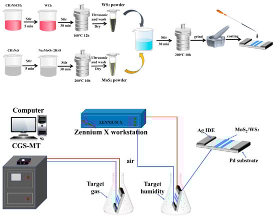
Figure 1.
The manufacturing process and testing process of the WS2/MoS2 sensor.
3. Results
Figure 2a,b illustrates the XRD analysis of the crystal structures of WS2 and MoS2, where 2θ is the diffraction angle. The spectrum of WS2 exhibits more distinct characteristic peaks at approximately 14.44° (002), 32.77° (100), 33.58° (101), 43.90° (103), and 58.42° (110), respectively, indicating that the WS2 sample belongs to 2H-WS2 (JCPDS:08-0237) [28]. The wide full width at half maxima and the weak peak intensity of WS2 implies the poor crystallinity of the sample. MoS2 peaks were located at 59.4° for the (110) plane, 32.7° for the (100) plane, and 14.44° for the (002) plane, respectively, corresponding to the 2H phase MoS2 (JCPDS:37-1492) [29] with good crystallinity. Furthermore, the MoS2/WS2 composites were analyzed through XRD analysis. In the composite samples, three distinct peaks were observed; the diffraction peak of the (002) (100) (110) crystal planes originated from MoS2, and (101) (103) (110) from WS2, respectively. This analysis demonstrated that the phase composition of the composite samples is a mixture of WS2 and MoS2 [30]. It has been observed that the peaks of the (002) crystal plane in the MoS2/WS2 composites exhibited a high intensity. The diffraction peak intensity of the composites gradually increased as the MoS2 composition increased, and the full width at half maxima narrowed, indicating that crystallinity improved as the relative concentration of MoS2 in the composites increased. At the same time, no other impurity peaks were detected in the XRD patterns, revealing that WS2 and MoS2 are chemically compatible [31].
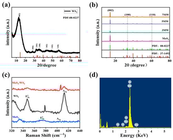
Figure 2.
(a,b) The XRD patterns of the prepared WS2, MoS2, and MoS2 /WS2 composites. (c) The Raman spectra of WS2, MoS2, and 5 MW. (d) The corresponding energy dispersive X-ray spectrum (EDS) of the 5 MW sample.
Figure 2c depicts the Raman spectra of WS2, MoS2, and 5 MW samples. Both WS2 and MoS2 have a hexagonal structure [32], and two main Raman resonance modes: E12g (in-plane phonons) and A1g (out-of-plane phonons). The resonance signals at 350.4, and 418.8 cm−1 in WS2 correspond to the E12g and A1g modes, whereas the signals at 376.6 cm−1 and 404.8 cm−1 in MoS2 correspond to the E12g and A1g modes, respectively. The XRD analysis and Raman spectra of the WS2 and MoS2 resonance signals confirmed the successful synthesis of the MoS2/WS2 composites [33]. The energy dispersive spectral analysis of the 5 MW sample depicted in Figure 2d reveals the presence of the elements S, Mo, and W.
The surface composition and chemical state of the MoS2/WS2 composite were determined using XPS analysis, and the results are shown in Figure 3. We used the C 1s peak of 284.8 eV as a reference for the binding energy. The characteristic peaks of S 2p, Mo 3d, Mo 3p, and W 4f were observed in the MoS2/WS2 composites from the broad scan spectrum (Figure 3a). High-resolution XPS spectra were employed to scan the orbital peaks of Mo 3d, W 4f, and S 2p, as demonstrated in Figure 3b–d. The S2 p3/2 and S2 p1/2 states in Figure 3b appeared at 162.8 and 164.2 eV binding energy, respectively. The Mo 3d5/2 and Mo 3d3/2 peaks in Figure 3c are located at 229.9 and 233 eV, respectively, and are attributed to the Mo4+ in MoS2 [34]. In addition, there was no Mo6+3d3/2 orbital peak at 236 eV in this spectra, indicating that the Mo element was not oxidized, but was converted to complete sulfide [35,36]. The W 4f spectrum in Figure 3d contains W 4f7/2, W 4f5/2, and W 5p3/2 peaks with binding energies at 33.4, 35.5, and 39.6 eV, respectively [37]. Colors that appearing in subfigures b–d are just to differentiate different fit peaks. The aforementioned results indicate that the 5 MW composite comprises the elements Mo, W, and S, implying the successful formation of this composite.
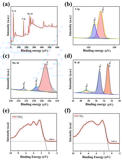
Figure 3.
The XPS spectra of the 5 MW sample: (a) the survey spectrum, (b) high-resolution S 2p, (c) high-resolution Mo 3d, (d) high-resolution W 4f of the 5 MW sample, and (e,f) the VB-XPS spectra of MoS2 and WS2.
In order to determine the valence band positions of MoS2 and WS2, first we assessed the Mott-Schottky curves of the materials to determine the positions of the Fermi energy levels, and the energies between the valence bands to the Fermi energy levels were determined by VB-XPS [38]. The XPS valence band scan depicted in Figure 3e,f revealed that the energy gaps between the maximum valence band (VBM) and the Fermi energy levels are 1.04 eV for MoS2 and 1.03 eV for WS2, respectively. The dashed lines in Figures e,f are background fit lines of VB-XPS, which is to obtain the energy between valence band and the Fermi level.
SEM images of WS2 in Figure 4a,b display a flake morphology with a thick and aggregated structure containing several grains attached to the surface. Figure 4c,d demonstrates that compared to the WS2 samples, MoS2 samples were less agglomerated and exhibited a flower-like morphology. Figure 4e–g displays the surface morphology of the 5 MW composite at different magnifications; the flower-like morphology can be observed more clearly in Figure 4g. Under high magnification SEM, the composite material displayed a lamellar structure. Figure 4f reveals that the 5 MW composite with a more uniform distribution exhibited a multilayer structure similar to that of the WS2 flakes, thereby providing more active sites for the desired gas absorption [39]. Figure 4h–j depicts the elemental mapping of the 5 MW composite, with a selected area shown in Figure 4g. In the 5 MW composites, S, Mo, and W were uniformly distributed, and no other elements were found.
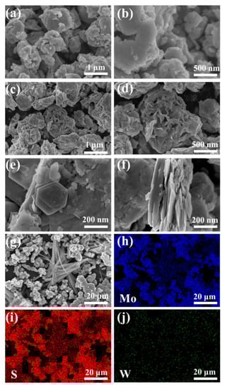
Figure 4.
The SEM images of (a,b) WS2. (c,d) MoS2, and (e–g) 5 MW. (h–j) The elemental mapping of the 5 MW sample.
The formation of MoS2/WS2 heterogeneous structures was confirmed using TEM. Figure 5a,b displays the 5 MW composite with a distinct ductile laminate structure. Figure 5c reveals a low-magnification TEM image of the heterostructure, where the light contrast outer layer was MoS2, while the inner layer was WS2. In addition, the magnified TEM image in Figure 5d depicts the interface between WS2 and MoS2, in which G, H, I are selected regions to progress further HRTEM analysis. Figure 5e,f represent the fast Fourier transform (FFT) patterns generated from the MoS2 and WS2, respectively (regions G and H in Figure 5). The same orientation and alignment of these diffraction points indicate an epitaxial relationship existing between MoS2 and WS2. However, the thickness of the MoS2 varies with the amount of MoS2 precursors utilized during the synthesis. HRTEM images of Figure 5g–i corresponds to the region depicted in the (G,H,I) region of Figure 5d, where uniform lattices with a spacing of 0.174 nm and 0.282 nm are observed, corresponding to the (100) and (010) planes of MoS2. The dotted stripe of 0.612 nm corresponds to the WS2 (002) plane (Figure 5e). The clear interface observed between WS2 and MoS2 in Figure 5d indicates a semiconductor heterojunction structure formation. The semiconductor heterojunction structure improves the electron-hole separation and transport properties, thereby enhancing the response speed of the gas sensors [40].
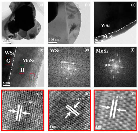
Figure 5.
TEM images (a–d) and HRTEM images (g–i) of the 5 MW nanosheets; (e,f) are the FFT diffraction patterns of the dashed boxes (G,H region in (d)), which corresponds to the MoS2 and WS2 components, respectively.
The UV-Vis absorption spectra and Tauc plots of the WS2, MoS2, 3 MW, 5 MW, and 7 MW samples are depicted in Figure 6a–d. The MoS2 and 3 MW, 5 MW, and 7 MW samples jumped at 320 nm due to the inhomogeneous surface of MoS2, but this effect is very weak for the material forbidden band width. The composite samples exhibited strong light absorption near 310–600 nm in the visible and ultraviolet spectra. It is evident that increasing the MoS2 content improves the absorption of the 3 MW, 5 MW, and 7 MW samples in the 400–760 nm range. Furthermore, the absorption edge of WS2 shifted to the visible region (500–700 nm) after modification by MoS2, which may be caused by the coupling band between WS2 and MoS2 and leads to a reduction in the exciton recombination time [41]. Figure 6b,d demonstrate the energy band gaps for the samples; the energy band gap Eg was calculated using the well-known Tauc plot. The calculation is performed as follows [42]:
where hv, α, k, and λ represent the photoelectron energy, absorption coefficient, absorption index, and wavelength of the photon, respectively, while n denotes the semiconductor type. In this work, the indirect transition was allowed [43]; therefore, n = 2. The calculated bandgaps of MoS2 and WS2 were 1.32 and 1.39 eV, respectively. It can also be determined according to the absorption edge, which was consistent with the bandgap calculated through the tangent. The bandgap of MoS2/WS2 composites became narrower as the MoS2 content increased, which facilitates the excitation of electrons from the valence band to the conduction band.
(αhv)1/n = A(hv − Eg)
α = 4πk/λ
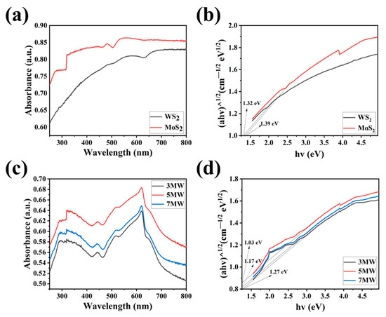
Figure 6.
(a,c) The UV-Vis absorption spectra of the WS2, MoS2, 3 MW, 5 MW, and 7 MW samples. (b,d) Tauc plots showing the band gaps of the WS2, MoS2, 3 MW, 5 MW, and 7 MW samples.
The capacitance–voltage (C-V) relationship curves of the samples were measured with an electrochemical workstation (CHI-660E). The Mott-Schottky (M-S) curve was plotted with C−2 as the vertical axis and swept voltage as the horizontal axis. The slope of the most extended straight-line part of the curve determines the type of conductivity of the semiconductor [44]. Figure 7 depicts the Mott-Schottky curves for the pure-phase WS2, MoS2, and MoS2/WS2 composite solid powder samples. The Mott-Schottky slopes for the WS2 and MoS2 samples were positive, indicating that they are n-type semiconductors. The flat-band potentials (Fermi energy levels) were determined to be −0.16 V and −0.12 V, respectively (vs. NHE, pH = 7), by extending the linear part of the Mott-Schottky curve to the potential axis. The Mott-Schottky slope was also found to be positive in the MoS2/WS2 composite, indicating that it is an n-type semiconductor, and the flat-band potential (Fermi energy level) was −0.02 V (vs. NHE, pH = 7). An n-n heterojunction at the MoS2 and WS2 contact interface was confirmed using TEM analysis. This is consistent with the measurement results of the gas-sensing properties. When the VB-XPS result was combined with the Fermi energy levels of −0.16 V and −0.12 V, determined by Mott-Schottky analysis, the valence band positions for MoS2 and WS2 were calculated to be 0.88 V and 0.91 V, respectively. According to the UV-Vis absorption spectra, the band gap of WS2 was 1.39 eV, and that of MoS2 was 1.32 eV, respectively. The conduction bands of MoS2 and WS2 were located at −0.44 V and −0.48 V, respectively.
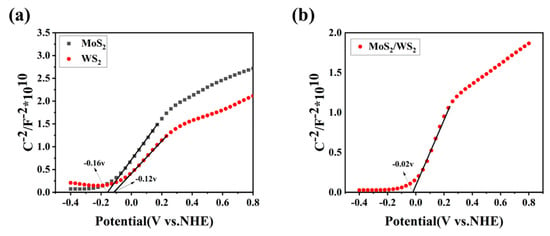
Figure 7.
(a,b) The Mott-Schottky curves for the MoS2, WS2, and 5 MW samples.
FT-IR spectral analysis reveals the surface chemical information and the vibrational modes of the chemical bonds present in the samples. Figure 8a–e depicts the IR spectra of MoS2, WS2, and their composite samples with varying relative mass ratios, revealing the surface functional groups. For WS2, the stretching vibrations of the W-S bond peak were located at approximately 2950 and 582 cm−1, respectively. Additionally, the S-S bond was at 1051 and 876 cm−1, respectively [45,46]. MoS2 exhibited typical Mo-S bond vibrations, with an absorption peak at 465 cm−1 [47]. The H-O-H bending motion and the O-H stretching vibrations of the adsorbed water on the surface of the composite were reflected at the peaks of 1626 and 3430 cm−1, respectively [48,49]. The broad peak at 3430 cm−1 was attributed to the symmetric and asymmetric O-H bond stretching patterns, which was more obvious in the composite material compared to the pure phases of WS2 and MOS2. This is advantageous for the detection of NH3, as the hydroxyl group has gas adsorption capacity, and improves the selectivity in the detection of NH3 due to the hydroxyl group's ability to hydrogen bond and weakly interact with ammonia, where the hydrogen molecules of ammonia combine with the oxygen molecules on the hydroxyl group to form a new chemical bond, thus allowing the ammonia to stay on the surface of the material for a longer period of time, which in turn improves the response of the material to NH3 [50]. The peaks of the W-S, S-S, Mo-S, O-H, and H-O-H bonds in MoS2/WS2 composites were derived from the MoS2 and WS2 components. Furthermore, the slight variation in the spectral shape (Figure 8c–e) indicates that the same groups were observed in different composite samples. The increased number of hydroxyl groups indicates that the composites possess better NH3 sensitivity properties than the pure phase.
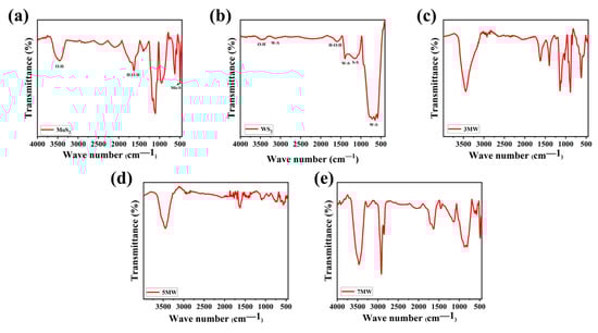
Figure 8.
The FT-IR spectra of the (a) MoS2, (b) WS2, (c) 3 MW, (d) 5 MW, (e) 7 MW samples.
The dynamic responses of the WS2, MoS2, and MoS2/WS2 composites to formaldehyde (HCHO), ethanol (C2H6O), ammonia (NH3), acetone (C3H6O), and hydrogen peroxide (H2O2) at room temperature are illustrated in Figure 9. The baseline current corresponds to an ambient test curve at approximately 30% RH (relative air humidity). The gas-sensing properties were obtained after three complete testing cycles, with the concentrations of all gases having been set to 500 ppm. Figure 9 demonstrates that the current response of the gas sensor increased rapidly when exposed to the vapors of HCHO, C2H6O, NH3, C3H6O, and H2O2. The response time is the time required to reach 90% of the maximum response current when the sensor is placed in the target gas, whereas the recovery is defined as the period of time when the sensor current changes to 10% of the response after removing the target gas. The response recovery curve in the figure reflects the n-type semiconductor’s characteristics. In our tests we found that MoS2 sometimes shows a negative response. This is because MoS2 is an n-type semiconductor, which is inevitably disturbed by ambient humidity during the performance test, and the adsorption of water molecules on the MoS2 surface equates to a p-type doping. As a result, the electrical properties change accordingly, and thus these samples show a response similar to the p-type semiconductor-based gas sensor in the reducing gas [51]. The responses of the pristine MoS2 and WS2-based sensors to NH3 were approximately 320% and 90%, respectively; while both WS2 and MoS2 exhibited a low NH3 response. The performance of composite-based sensors to HCHO, C2H6O, NH3, and C3H6O was also investigated at room temperature. The 5 MW samples outperformed WS2 and MoS2 in terms of detection performance to 500 ppm NH3 at a test voltage of 1 V, with a response of 23643%, enhanced by two orders of magnitude. Additionally, the 5 MW samples exhibited 2200%, 2310%, 672%, and 120% responses for other gases such as H2O2, C3H6O, HCHO, and C2H6O, respectively, indicating a good selectivity for the detection of targeted NH3 gases. The recovery time of the composite samples was particularly fast, with a relatively long response time for the detection of these five gases. The 5 MW composite exhibited a response time of 30 s and a recovery time of 2.6 s. The 5 MW samples demonstrated a good reproducibility for NH3 detection after consecutive test cycles. These results reveal that the prepared 5 MW samples are excellent for NH3 detection at room temperature, and that the introduction of composite components improves the gas-sensing properties of pristine WS2 or MoS2 samples.
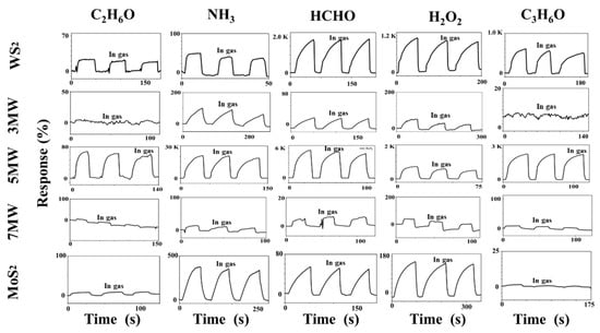
Figure 9.
Responses of MoS2, WS2, and their composites to different gases (C2H6O, NH3, HCHO, H2O2, and C3H6O, respectively) of 500 ppm, 30% RH at room temperature.
The selectivity plots of WS2, MoS2 and MoS2/WS2 composites for HCHO, C2H6O, NH3, C3H6O, and H2O2 gases are depicted in Figure 10a. When compared to other composite samples, the response of the 5 MW sample to NH3 reached nearly four orders of magnitude higher, demonstrating that the 5 MW samples exhibit a high selectivity for NH3 detection. The histogram of response/recovery time is shown in Figure 10b. Compared with other samples, the 5 MW composite had a response time of about 30 s and a recovery time of only 2.6 s, revealing an efficient detection performance and a fast recovery for NH3 detection. Figure 10c,d depicts the response versus different concentrations of NH3 at room temperature. The current response of the 5 MW gas sensor increases with increasing NH3 concentration, which can be attributed to the increased possibility of gas adsorption at the active sites on the sample surface. In addition, the 5 MW gas sensor exhibits a highly linear relationship for NH3 detection in the concentration range of 20–500 ppm. The linear relation was as follows: R = 0.39287C + 15.60856 (R2 = 0.98137 in Figure 10e). Figure 10f exhibits a six-month response comparison of the 5 MW sensor to 500 ppm NH3 at room temperature. The response reaches four orders of magnitude both before and after six months, confirming the excellent long-term stability of the 5 MW gas sensor.
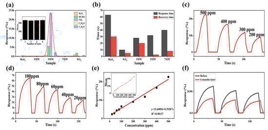
Figure 10.
(a) Selectivity of MoS2, WS2, and composite samples for different gases of 500 ppm at room temperature. (b) Response and recovery time of the 5 MW-based gas sensor to 500 ppm NH3 at room temperature. (c,d) Responses of the 5 MW sample to different concentrations of NH3 at room temperature. (e) Linear response of the 5 MW sensor to varying concentrations of NH3. (f) Long-term stability of the 5 MW sensor for six months.
Humidity immunity tests were performed to eliminate humidity interference with the gas sensor. The prepared sensors were placed in chambers with different humidity levels (11–95% RH) by rapidly switching the sensors from one chamber to another. Impedance versus humidity curves for the pristine MoS2 and WS2 at 100 Hz, AC 1 V are displayed in Figure 11a. The response was less than one order of magnitude for MoS2 and one order of magnitude for WS2 over the humidity range of 11–95% RH. Figure 11b reveals that the 5 MW composite exhibited excellent humidity immunity, and the moisture-sensitive response was less than an order of magnitude. These results indicate that both the pure-phase and composite samples had a high humidity resistance.
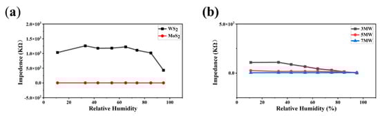
Figure 11.
(a) Response curves of the MoS2, WS2 samples to 11–95% RH; (b) Response curves of the MoS2/WS2 composites to 11–95% RH.
Table 1 summarizes the performance of NH3 sensors reported in the literature in recent years. Compared to the previous studies, the 5 MW composite prepared in this work exhibits a shorter recovery time (2.6 s), and a higher response of 23643% to 500 ppm NH3.

Table 1.
Comparison of sensing parameters of the 5 MW sensor with previously reported sensors.
4. Discussion
The energy band was determined by combining the Mott-Schottky curve, XPS valence band spectrum, and UV-visible absorption spectrum, as illustrated in Figure 12. As demonstrated through the previous analysis, the slopes of Mott-Schottky curves of WS2, MoS2 and MoS2/WS2 samples were all positive, implying that the prepared samples are n-type semiconductors, while the TEM analysis demonstrated that heterostructures were formed between the two components. In particular, n-n-type MoS2/WS2 heterostructures were developed in this study, which are commensurate with the adsorption–desorption curve characteristics of WS2, MoS2, and MoS2/WS2 sensors. The electrons would be transferred between MoS2 and WS2 until the Fermi energy level reaches equilibrium.
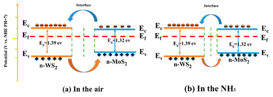
Figure 12.
The sensing mechanism of the MoS2/ WS2 gas sensor in (a) air and (b) NH3.
The NH3 gas-sensitive mechanism of the MoS2/WS2 sensor was explained using a surface resistance control model, which included the change in the sensor resistance due to the redox reaction between the chemisorbed oxygen and the target gas molecules [57]. When the MoS2/WS2 composite was exposed to air at room temperature, O2 molecules were adsorbed on the sample surface, and free electrons on the composite surface were captured by O2 to produce surface adsorbed species (O2−, O−, O2−), as illustrated in Figure 12a. The corresponding reaction processes are described in Equations (1) and (2) [58].
O2 (gas) → O2 (adsorption)
O2 (adsorption) + e− → O2− (adsorption) (<100 °C)
At this point, a wide depletion layer has been formed on the sample surface due to a severe lack of electrons, while the sensor’s resistance is high. When the MoS2/WS2 composite is exposed to NH3, the reducing gas interacts with the adsorbed O2− to produce H2O, N2, and free electrons, according to Equations (3) and (4).
NH3 (gas) ↔ NH3 (adsorption)
4NH3 (adsorption) + 3O2− (adsorption) → 6H2O + 2N2 + 3e−
The captured electrons are subsequently returned to the sample surface. This process significantly reduces the thickness of the electron depletion layer. As a result, the electron depletion layer narrows, and the resistance reduces (Figure 12b).
The development of the heterojunction was deemed to be the main reason for the enhanced gas-sensitive response. As previously demonstrated, WS2 and MoS2 are n-type semiconductors with electrons as the main charge carriers. The Fermi energy level of MoS2 was higher than that of WS2, as illustrated by the Mott-Schottky curves. Electrons would be transported in the air from MoS2 to WS2 until the Fermi energy levels reached equilibrium. In contrast, carriers (holes) leaving the valence band would diffuse in the opposite direction to achieve effective charge-carrier separation. Consequently, the energy band bends, creating a barrier that impedes electron transport. Therefore, the baseline resistance of the WS2/MoS2 sensors significantly increased. The resistance was further reduced when the sensor was placed in NH3 since the electrons released by the reaction with O2− lowered the potential barrier in the heterojunction region. Therefore, the sensing performance of MoS2/WS2 composites to NH3 was enhanced due to the substantial change in device resistance [59,60].
On the other hand, the superior sensing performance of the MoS2/WS2 composites over pristine WS2 and MoS2 can be attributed to the flower-like morphology of the WS2/MoS2 composites compared to the homogeneous sheet-like morphology of pure-phase WS2 and MoS2, which provides more active sites for surface reactions and promotes gas adsorption and desorption, thus improving the gas-sensing response.
In short, the excellent gas-sensing properties of MoS2/WS2 composites are attributed to the gain effect of the n-n heterojunction and unique surface morphology.
5. Conclusions
In this study, MoS2/WS2 composites were prepared using a one-step hydrothermal method that is highly adaptable, affordable, and accessible. A heterostructure was successfully formed by controlling the relative mass ratio of WS2 and MoS2, revealing carrier movement and transformation at the MoS2/WS2 interface. The positions of the valence and conduction bands of the two-component semiconductors were determined by the Mott-Schottky curves, UV-Vis spectra, and XPS valence band spectra. Afterward, WS2-MoS2 heterojunction-based gas-sensitive sensors were fabricated. The 5 MW sample exhibited good gas-sensitive characteristics when the relative mass ratio of MoS2 and WS2 was 50 wt% with a response of 23643% for 500 ppm NH3 gas, a fast recovery time of 2.6 s, a detection limit of 20 ppm, and long-term stability for six months. The humidity immune test demonstrated that the 5 MW sample possesses good moisture resistance in the humidity range of 11–95% RH. This work provides an approach for the simple and low-cost preparation of two-dimensional gas-sensing materials with heterostructures. It also provides a facile way to obtain NH3 gas sensors working at room temperature.
Author Contributions
M.Z. and J.Z. conceived and designed the experiments, J.Z. performed the experiments, M.Z. and J.Z. analyzed the data and wrote the paper. All authors have read and agreed to the published version of the manuscript.
Funding
This research was funded by the National Natural Science Foundation of China (Grant Nos. 22262033), and the Natural Science Foundation of Xinjiang Uygur Autonomous Region (2021D01C031).
Data Availability Statement
The data presented in this study are available on request from the corresponding author.
Conflicts of Interest
The authors declare no conflict of interest.
References
- Krupa, S.V. Effects of atmospheric ammonia (NH3) on terrestrial vegetation: A review. Environ. Pollut. 2003, 124, 179–221. [Google Scholar] [CrossRef] [PubMed]
- Boron, W.F.; De Weer, P. Intracellular pH transients in squid giant axons caused by CO2, NH3, and metabolic inhibitors. J. Gen. Physiol. 1976, 67, 91–112. [Google Scholar] [CrossRef] [PubMed]
- Li, J.; Chang, H.; Ma, L.; Hao, J.; Yang, R.T. Low-temperature selective catalytic reduction of NOx with NH3 over metal oxide and zeolite catalysts—A review. Catal. Today 2011, 175, 147–156. [Google Scholar] [CrossRef]
- Sufriadi, E.; Meilina, H.; Munawar, A.A.; Muhammad, S.; Idroes, R. Identification of β-Caryophyllene (BCP) in Aceh Patchouli Essential Oil (PEO) using Gas Chromatography-Mass Pectrophotometry (GC-MS), IOP Conference Series: Earth and Environmental Science, 2021; IOP Publishing: Bristol, UK, 2021; p. 12032. [Google Scholar]
- Bartle, K.D.; Myers, P. History of gas chromatography. TrAC Trends Anal. Chem. 2002, 21, 547–557. [Google Scholar] [CrossRef]
- Bakker, E.; Telting-Diaz, M. Electrochemical sensors. Anal. Chem. 2002, 74, 2781–2800. [Google Scholar] [CrossRef]
- Fine, G.F.; Cavanagh, L.M.; Afonja, A.; Binions, R. Metal oxide semi-conductor gas sensors in environmental monitoring. Sensors-Basel 2010, 10, 5469–5502. [Google Scholar] [CrossRef]
- Nikolic, M.V.; Milovanovic, V.; Vasiljevic, Z.Z.; Stamenkovic, Z. Semiconductor gas sensors: Materials, technology, design, and application. Sensors 2020, 20, 6694. [Google Scholar] [CrossRef]
- Gu, J.; Chakraborty, B.; Khatoniar, M.; Menon, V.M. A room-temperature polariton light-emitting diode based on monolayer WS2. Nat. Nanotechnol. 2019, 14, 1024–1028. [Google Scholar] [CrossRef]
- Kim, J.; Mirzaei, A.; Kim, H.W.; Kim, S.S. Realization of Au-decorated WS2 nanosheets as low power-consumption and selective gas sensors. Sens. Actuators B Chem. 2019, 296, 126659. [Google Scholar] [CrossRef]
- Sharma, S.; Saini, R.; Gupta, G.; Late, D.J. Room-temperature highly sensitive and selective NH3 gas sensor using vertically aligned WS2 nanosheets. Nanotechnology 2022, 34, 45704. [Google Scholar] [CrossRef]
- Xu, P.; Cheng, Z.; Pan, Q.; Xu, J.; Xiang, Q.; Yu, W.; Chu, Y. High aspect ratio In2O3 nanowires: Synthesis, mechanism and NO2 gas-sensing properties. Sens. Actuators B Chem. 2008, 130, 802–808. [Google Scholar] [CrossRef]
- Qin, Z.; Song, X.; Wang, J.; Li, X.; Wu, C.; Wang, X.; Yin, X.; Zeng, D. Development of flexible paper substrate sensor based on 2D WS2 with S defects for room-temperature NH3 gas sensing. Appl. Surf. Sci. 2022, 573, 151535. [Google Scholar] [CrossRef]
- Yu, S.M.; Kim, J.H.; Yoon, K.R.; Jung, J.W.; Oh, J.H.; Kim, I.D. Single Layers of WS2 Nanoplates Anchored to Hollow N-Doped Carbon Nanofibers as Efficient Electrocatalysts for Hydrogen Evolution, 2015 Fall MRS, 2015; Materials Research Society: Warrendale, PA, USA, 2015. [Google Scholar]
- Zhao, F.; Li, Z.; Fu, Y.; Wang, Q. Gas-Sensitive Characteristics of Graphene Composite Tungsten Disulfide to Ammonia. Sensors 2022, 22, 8672. [Google Scholar] [CrossRef] [PubMed]
- Järvinen, T.; Lorite, G.S.; Peräntie, J.; Toth, G.; Saarakkala, S.; Virtanen, V.K.; Kordas, K. WS2 and MoS2 thin film gas sensors with high response to NH3 in air at low temperature. Nanotechnology 2019, 30, 405501. [Google Scholar] [CrossRef] [PubMed]
- Late, D.J.; Kanawade, R.V.; Kannan, P.K.; Rout, C.S. Atomically thin WS2 nanosheets based gas sensor. Sens. Lett. 2016, 14, 1249–1254. [Google Scholar] [CrossRef]
- Perrozzi, F.; Emamjomeh, S.M.; Paolucci, V.; Taglieri, G.; Ottaviano, L.; Cantalini, C. Thermal stability of WS2 flakes and gas sensing properties of WS2/WO3 composite to H2, NH3 and NO2. Sens. Actuators B Chem. 2017, 243, 812–822. [Google Scholar] [CrossRef]
- Luo, H.; Shi, J.; Liu, C.; Chen, X.; Lv, W.; Zhou, Y.; Zeng, M.; Yang, J.; Wei, H.; Zhou, Z. Design of p–p heterojunctions based on CuO decorated WS2 nanosheets for sensitive NH3 gas sensing at room temperature. Nanotechnology 2021, 32, 445502. [Google Scholar] [CrossRef]
- Ouyang, C.; Chen, Y.; Qin, Z.; Zeng, D.; Zhang, J.; Wang, H.; Xie, C. Two-dimensional WS2-based nanosheets modified by Pt quantum dots for enhanced room-temperature NH3 sensing properties. Appl. Surf. Sci. 2018, 455, 45–52. [Google Scholar] [CrossRef]
- Singh, S.; Saggu, I.S.; Chen, K.; Xuan, Z.; Swihart, M.T.; Sharma, S. Humidity-tolerant room-temperature selective dual sensing and discrimination of NH3 and no using a WS2/MWCNT Composite. ACS Appl. Mater. Inter. 2022, 14, 40382–40395. [Google Scholar] [CrossRef]
- Paolucci, V.; Emamjomeh, S.M.; Ottaviano, L.; Cantalini, C. Near room temperature light-activated WS2-decorated rGO as NO2 gas sensor. Sensors 2019, 19, 2617. [Google Scholar] [CrossRef]
- Yadav, A.A.; Hunge, Y.M.; Kang, S. Visible Light-Responsive CeO2/MoS2 Composite for Photocatalytic Hydrogen Production. Catalysts 2022, 12, 1185. [Google Scholar] [CrossRef]
- Hunge, Y.M.; Yadav, A.A.; Kang, S.; Lim, S.J.; Kim, H. Visible light activated MoS2/ZnO composites for photocatalytic degradation of ciprofloxacin antibiotic and hydrogen production. J. Photochem. Photobiol. A Chem. 2023, 434, 114250. [Google Scholar] [CrossRef]
- Hunge, Y.M.; Yadav, A.A.; Kang, S. Photocatalytic Degradation of Eriochrome Black-T Using BaWO4/MoS2 Composite. Catalysts 2022, 12, 1290. [Google Scholar] [CrossRef]
- Zhang, J.; Wang, J.; Chen, P.; Sun, Y.; Wu, S.; Jia, Z.; Lu, X.; Yu, H.; Chen, W.; Zhu, J. Observation of strong interlayer coupling in MoS2/WS2 heterostructures. Adv. Mater. 2016, 28, 1950–1956. [Google Scholar] [CrossRef] [PubMed]
- Vikraman, D.; Hussain, S.; Akbar, K.; Truong, L.; Kathalingam, A.; Chun, S.; Jung, J.; Park, H.J.; Kim, H. Improved hydrogen evolution reaction performance using MoS2–WS2 heterostructures by physicochemical process. ACS Sustain. Chem. Eng. 2018, 6, 8400–8409. [Google Scholar] [CrossRef]
- Yu, Y.; Hu, S.; Su, L.; Huang, L.; Liu, Y.; Jin, Z.; Purezky, A.A.; Geohegan, D.B.; Kim, K.W.; Zhang, Y. Equally efficient interlayer exciton relaxation and improved absorption in epitaxial and nonepitaxial MoS2/WS2 heterostructures. Nano Lett. 2015, 15, 486–491. [Google Scholar] [CrossRef] [PubMed]
- Chen, H.; Wen, X.; Zhang, J.; Wu, T.; Gong, Y.; Zhang, X.; Yuan, J.; Yi, C.; Lou, J.; Ajayan, P.M. Ultrafast formation of interlayer hot excitons in atomically thin MoS2/WS2 heterostructures. Nat. Commun. 2016, 7, 12512. [Google Scholar] [CrossRef]
- Chen, S.; Pan, Y. Enhancing catalytic properties of noble metal@ MoS2/WS2 heterojunction for the hydrogen evolution reaction. Appl. Surf. Sci. 2022, 591, 153168. [Google Scholar] [CrossRef]
- Deilmann, T.; Thygesen, K.S. Interlayer trions in the MoS2/WS2 van der Waals heterostructure. Nano Lett. 2018, 18, 1460–1465. [Google Scholar] [CrossRef]
- Kaushik, V.; Ahmad, M.; Agarwal, K.; Varandani, D.; Belle, B.D.; Das, P.; Mehta, B.R. Charge transport in 2D MoS2, WS2, and MoS2–WS2 heterojunction-based field-effect transistors: Role of ambipolarity. J. Phys. Chem. C 2020, 124, 23368–23379. [Google Scholar] [CrossRef]
- Chiappe, D.; Asselberghs, I.; Sutar, S.; Iacovo, S.; Afanas’ Ev, V.; Stesmans, A.; Balaji, Y.; Peters, L.; Heyne, M.; Mannarino, M. Controlled sulfurization process for the synthesis of large area MoS2 films and MoS2/WS2 heterostructures. Adv. Mater. Interfaces 2016, 3, 1500635. [Google Scholar] [CrossRef]
- Sharma, A.; Mahlouji, R.; Wu, L.; Verheijen, M.A.; Vandalon, V.; Balasubramanyam, S.; Hofmann, J.P.; Kessels, W.E.; Bol, A.A. Large area, patterned growth of 2D MoS2 and lateral MoS2–WS2 heterostructures for nano-and opto-electronic applications. Nanotechnology 2020, 31, 255603. [Google Scholar] [CrossRef] [PubMed]
- Hong, X.; Kim, J.; Shi, S.; Zhang, Y.; Jin, C.; Sun, Y.; Tongay, S.; Wu, J.; Zhang, Y.; Wang, F. Ultrafast charge transfer in atomically thin MoS2/WS2 heterostructures. Nat Nanotechnol 2014, 9, 682–686. [Google Scholar] [CrossRef] [PubMed]
- Xiong, Y.F.; Chen, J.H.; Lu, Y.Q.; Xu, F. Broadband optical-fiber-compatible photodetector based on a graphene-MoS2-WS2 heterostructure with a synergetic photogenerating mechanism. Adv. Electron. Mater. 2019, 5, 1800562. [Google Scholar] [CrossRef]
- Tang, M.; Zhang, D.; Wang, D.; Deng, J.; Kong, D.; Zhang, H. Performance prediction of 2D vertically stacked MoS2-WS2 heterostructures base on first-principles theory and Pearson correlation coefficient. Appl. Surf. Sci. 2022, 596, 153498. [Google Scholar] [CrossRef]
- Zhao, X.; Tang, G.; Li, Y.; Zhang, M.; Nie, Y. Biaxial strain improving the thermoelectric performance of a two-dimensional MoS2/WS2 heterostructure. ACS Appl. Electron. Ma 2021, 3, 2995–3004. [Google Scholar] [CrossRef]
- Zhang, X.; Huangfu, L.; Gu, Z.; Xiao, S.; Zhou, J.; Nan, H.; Gu, X.; Ostrikov, K. Controllable Epitaxial Growth of Large-Area MoS2/WS2 Vertical Heterostructures by Confined-Space Chemical Vapor Deposition. Small 2021, 17, 2007312. [Google Scholar] [CrossRef]
- Choudhary, N.; Park, J.; Hwang, J.Y.; Chung, H.; Dumas, K.H.; Khondaker, S.I.; Choi, W.; Jung, Y. Centimeter scale patterned growth of vertically stacked few layer only 2D MoS2/WS2 van der Waals heterostructure. Sci. Rep. 2016, 6, 1–7. [Google Scholar] [CrossRef]
- Pesci, F.M.; Sokolikova, M.S.; Grotta, C.; Sherrell, P.C.; Reale, F.; Sharda, K.; Ni, N.; Palczynski, P.; Mattevi, C. MoS2/WS2 heterojunction for photoelectrochemical water oxidation. ACS Catal. 2017, 7, 4990–4998. [Google Scholar] [CrossRef]
- Wang, L.; Tahir, M.; Chen, H.; Sambur, J.B. Probing charge carrier transport and recombination pathways in monolayer MoS2/WS2 heterojunction photoelectrodes. Nano Lett. 2019, 19, 9084–9094. [Google Scholar] [CrossRef]
- Lin, Z.; Luo, P.; Zeng, W.; Lai, H.; Xie, W.; Deng, W.; Luo, Z. Improvement of photoelectric properties of MoS2/WS2 heterostructure photodetector with interlayer of Au nanoparticles. Opt. Mater. 2020, 108, 110191. [Google Scholar] [CrossRef]
- Zhang, X.; Xiao, S.; Nan, H.; Mo, H.; Wan, X.; Gu, X.; Ostrikov, K.K. Controllable one-step growth of bilayer MoS2–WS2/WS2 heterostructures by chemical vapor deposition. Nanotechnology 2018, 29, 455707. [Google Scholar] [CrossRef] [PubMed]
- Kang, J.; Sahin, H.; Peeters, F.M. Tuning carrier confinement in the MoS2/WS2 lateral heterostructure. J. Phys. Chem. C 2015, 119, 9580–9586. [Google Scholar] [CrossRef]
- Xue, Y.; Zhang, Y.; Liu, Y.; Liu, H.; Song, J.; Sophia, J.; Liu, J.; Xu, Z.; Xu, Q.; Wang, Z. Scalable production of a few-layer MoS2/WS2 vertical heterojunction array and its application for photodetectors. ACS Nano 2016, 10, 573–580. [Google Scholar] [CrossRef]
- Shan, J.; Li, J.; Chu, X.; Xu, M.; Jin, F.; Fang, X.; Wei, Z.; Wang, X. Enhanced photoresponse characteristics of transistors using CVD-grown MoS2/WS2 heterostructures. Appl. Surf. Sci. 2018, 443, 31–38. [Google Scholar] [CrossRef]
- Zeng, Y.; Dai, W.; Ma, R.; Li, Z.; Ou, Z.; Wang, C.; Yu, Y.; Zhu, T.; Liu, X.; Wang, T. Distinguishing Ultrafast Energy Transfer in Atomically Thin MoS2/WS2 Heterostructures. Small 2022, 18, 2204317. [Google Scholar] [CrossRef]
- Wang, F.; Wang, J.; Guo, S.; Zhang, J.; Hu, Z.; Chu, J. Tuning coupling behavior of stacked heterostructures based on MoS2, WS2, and WSe2. Sci. Rep. 2017, 7, 1–10. [Google Scholar] [CrossRef]
- Wang, J.; Li, Z.; Zhang, S.; Yan, S.; Cao, B.; Wang, Z.; Fu, Y. Enhanced NH3 gas-sensing performance of silica modified CeO2 nanostructure based sensors. Sens. Actuators B Chem. 2018, 255, 862–870. [Google Scholar] [CrossRef]
- Zhao, J.; Li, N.; Yu, H.; Wei, Z.; Liao, M.; Chen, P.; Wang, S.; Shi, D.; Sun, Q.; Zhang, G. Highly sensitive MoS2 humidity sensors array for noncontact sensation. Adv. Mater. 2017, 29, 1702076. [Google Scholar] [CrossRef]
- Kim, T.; Lee, T.H.; Park, S.Y.; Eom, T.H.; Cho, I.; Kim, Y.; Kim, C.; Lee, S.A.; Choi, M.; Suh, J.M. Drastic Gas Sensing Selectivity in 2-Dimensional MoS2 Nanoflakes by Noble Metal Decoration. Acs Nano 2023, 17, 4404–4413. [Google Scholar] [CrossRef]
- Lee, E.; VahidMohammadi, A.; Prorok, B.C.; Yoon, Y.S.; Beidaghi, M.; Kim, D. Room temperature gas sensing of two-dimensional titanium carbide (MXene). ACS Appl. Mater. Inter. 2017, 9, 37184–37190. [Google Scholar] [CrossRef] [PubMed]
- Rabchinskii, M.K.; Sysoev, V.V.; Glukhova, O.E.; Brzhezinskaya, M.; Stolyarova, D.Y.; Varezhnikov, A.S.; Solomatin, M.A.; Barkov, P.V.; Kirilenko, D.A.; Pavlov, S.I. Guiding Graphene Derivatization for the On-Chip Multisensor Arrays: From the Synthesis to the Theoretical Background. Adv. Mater. Technol. 2022, 7, 2101250. [Google Scholar] [CrossRef]
- Zhang, H.; Wang, L.; Zou, Y.; Li, Y.; Xuan, J.; Wang, X.; Jia, F.; Yin, G.; Sun, M. Enhanced ammonia sensing response based on Pt-decorated Ti3C2Tx/TiO2 composite at room temperature. Nanotechnology 2023, 34, 205501. [Google Scholar] [CrossRef]
- Liu, Z.; Han, D.; Liu, L.; Li, D.; Han, X.; Chen, Y.; Liu, X.; Zhuo, K.; Cheng, Y.; Sang, S. Ultrasensitive ammonia gas sensor based on Ti3C2Tx/Ti3AlC2 planar composite at room temperature. Sens. Actuators B Chem. 2023, 378, 133149. [Google Scholar] [CrossRef]
- Wang, L.; Meng, W.; He, Z.; Meng, W.; Li, Y.; Dai, L. Enhanced selective performance of mixed potential ammonia gas sensor by Au nanoparticles decorated CeVO4 sensing electrode. Sens. Actuators B Chem. 2018, 272, 219–228. [Google Scholar] [CrossRef]
- Rigosi, A.F.; Hill, H.M.; Li, Y.; Chernikov, A.; Heinz, T.F. Probing interlayer interactions in transition metal dichalcogenide heterostructures by optical spectroscopy: MoS2/WS2 and MoSe2/WSe2. Nano Lett. 2015, 15, 5033–5038. [Google Scholar] [CrossRef] [PubMed]
- Bogaert, K.; Liu, S.; Chesin, J.; Titow, D.; Gradecak, S.; Garaj, S. Diffusion-mediated synthesis of MoS2/WS2 lateral heterostructures. Nano Lett. 2016, 16, 5129–5134. [Google Scholar] [CrossRef]
- He, X.; Li, H.; Zhu, Z.; Dai, Z.; Yang, Y.; Yang, P.; Zhang, Q.; Li, P.; Schwingenschlogl, U.; Zhang, X. Strain engineering in monolayer WS2, MoS2, and the WS2/MoS2 heterostructure. Appl. Phys. Lett. 2016, 109, 173105. [Google Scholar] [CrossRef]


Disclaimer/Publisher’s Note: The statements, opinions and data contained in all publications are solely those of the individual author(s) and contributor(s) and not of MDPI and/or the editor(s). MDPI and/or the editor(s) disclaim responsibility for any injury to people or property resulting from any ideas, methods, instructions or products referred to in the content. |
© 2023 by the authors. Licensee MDPI, Basel, Switzerland. This article is an open access article distributed under the terms and conditions of the Creative Commons Attribution (CC BY) license (https://creativecommons.org/licenses/by/4.0/).