1. Introduction
With the increasing demands for implantable, wearable, portable electronics and Internet of Things (IoTs), miniature energy storage capacitors are essential for self-powered systems and instantaneous high-power output applications through monolithic three-dimensional (3D) integration with the back-end-of-line (BEOL) of integrated circuits, or system-in-package (SiP). Compared with electrochemical capacitors and micro-batteries, solid-state electrostatic capacitors can offer additional advantages, including a smaller volume, a higher power density and more charge/discharge cycles, especially under various extreme conditions, which makes them more suitable for miniaturized energy autonomous systems [
1,
2,
3]. So far, various dielectric materials such as inorganic perovskites, polymers and glass have been studied for electrostatic capacitors, but these materials encounter severe challenges for on-chip or 3D integrated capacitors due to their complex fabrication processes and poor compatibility with standard complementary metal–oxide–semiconductor (CMOS) technology [
4].
In recent years, various element-doped HfO
2 antiferroelectric (AFE) thin films such as Hf
xZr
1−xO
2 (0.1 ≤
x ≤ 0.4), HfAlO
x and HfSiO
x have been explored for the usage of on-chip electrostatic capacitors, showing high energy storage density (ESD) comparable or even superior to conventional perovskite materials [
5,
6,
7]. Meanwhile, the doped HfO
2 thin films can be grown via mature atomic layer deposition (ALD) processes at low temperatures of <350 °C. This guarantees its process compatibility with the BEOL of CMOS technology and processibility over 3D structures. Further, in combination with good reliability, excellent thermal stability and eco-friendly properties, the doped HfO
2 AFE dielectrics are considered to be very promising materials for on-chip energy storage applications [
8]. To improve the ESD of capacitors, our recent studies indicate that the employment of a 1 nm Hf
0.5Zr
0.5O
2 underlying layer between the bottom electrode and the AFE Hf
0.25Zr
0.75O
2 layer can promote the generation of the AFE tetragonal (T)-phase in the AFE layer [
9]. In addition, Yang et al. reported a HfO
2/ZrO
2 nanolaminate with a 2.2 nm HfO
2 thin film as the insertion layer between the TiN bottom electrode and ZrO
2 AFE thin film and achieved an ESD of up to 49.9 J cm
−3 [
10]. Therefore, the introduction of a dielectric layer between the AFE layer and the metal electrode is an effective way to increase the ESD. However, an undesired compromise between the ESD and energy storage efficiency (ESE) usually exists for most doped HfO
2 AFE capacitors [
8,
11,
12]. For example, the HfAlO
x AFE thin film demonstrated a maximal ESD of 63.7 J cm
−3, with an ordinary ESE of 64.2% at 6.5 MV cm
−1 [
6]. Moreover, an ESE as high as 93% was achieved for the Al:Hf
0.5Zr
0.5O
2 thin film, but the ESD was only 22 J cm
−3 [
13]. Thus, it has always been an ambitious goal to achieve doped HfO
2 AFE capacitors that simultaneously possess a high ESD and a high ESE. To enhance the ESE of the capacitors, it is reported that the stability of the T-phase can be improved by decreasing the free energy of the T-phase by reducing the deposition temperature of the Hf
xZr
1−xO
2 thin film to 210 °C [
11]. Moreover, the trace Al doping in HfO
2 thin films can improve the AFE behavior because of the enhanced electric field stability of the T-phase [
13]. In addition, Das et al. demonstrated an effective way to enrich the energy storage performance of single layer Hf
xZr
1−xO
2 capacitors by inserting an Al
2O
3 interlayer in the middle of the Hf
xZr
1−xO
2 thin films [
14]. However, there is still a relatively big room for improvement in the energy storage performance of doped HfO
2 AFE capacitors.
In this work, by doping the Al element in the Hf0.25Zr0.75O2 AFE layer accompanied by a 1 nm Hf0.5Zr0.5O2 underlying layer, an ultra-high ESD of 81.4 J cm−3 and a perfect ESE of 82.9% were achieved simultaneously, accompanied by a robust thermal stability and excellent electric field cycling endurance.
2. Materials and Methods
Capacitors consisting of W/Hf
0.5Zr
0.5O
2/Al-doped Hf
0.25Zr
0.75O
2 (HfZrO:Al)/W were fabricated on 300 nm SiO
2/Si substrates. The W top and bottom electrodes were deposited via direct current (DC) magnetron sputtering (ACS-4000-C4, ULVAC, Chigasaki, Japan) with a 100 W DC power at room temperature, a high purity tungsten target (>99.95%, ZhongNuo Advanced Material, Beijing, China) and an argon (Ar) gas flow of 20 sccm. The deposited W thin film was about 50 nm. Various nanostacks of 1 nm Hf
0.5Zr
0.5O
2/9 nm HfZrO:Al thin films were deposited via plasma-enhanced ALD (R-200 Advanced, Picosun, Masala, Finland) at 220 °C. The Hf[N(C
2H
5)CH
3]
4 (TEMAH, >99.99%, J&K Scientific, Beijing, China), Zr[N(CH
3)
2]
4 (TDMAZ, >99.99%, J&K Scientific) and Al(CH
3)
3 (TMA, >99.99%, J&K Scientific) were used as the precursors of Hf, Zr and Al, which were kept at 100 °C, 80 °C and 20 °C, respectively. The O
2 plasma served as the oxygen source, which was generated by a plasma generator integrated within the ALD equipment under 2500 W. In detail, one ALD cycle of HfO
2 or ZrO
2 included a 1.6 s vapor pulse of Hf or Zr precursor via an N
2 carrier gas (80 sccm) and a 10 s O
2 plasma pulse (130 sccm). Meanwhile, each pulse was followed by a 10 s N
2 (150 sccm) purging step to remove the excess precursors and post-reaction byproducts. For one ALD cycle of Al
2O
3, a 0.1 s TMA pulse via N
2 carrier gas (100 sccm) and a 0.1 s H
2O vapor pulse by means of N
2 carrier gas (150 sccm) were used. In this case, the growth rates of HfO
2 and ZrO
2 were both about 0.81 Å/cycle and the growth rate of Al
2O
3 was about 0.83 Å/cycle. The Hf
0.5Zr
0.5O
2 and Hf
0.25Zr
0.75O
2 thin films were deposited by fixing the ALD cycle ratios of HfO
2/ZrO
2 at 1:1 and 1:3, respectively. Therefore, according to the growth rates of HfO
2 and ZrO
2 thin films, a 1 nm Hf
0.5Zr
0.5O
2 thin film was fabricated by alternate deposition of 1 cycle of HfO
2 and 1 cycle of ZrO
2 for 6 times, and a 9 nm Hf
0.25Zr
0.75O
2 thin film was prepared by alternate growth of 1 cycle of HfO
2 and 3 cycles of ZrO
2 for 27 times. It deserves to be mentioned that the doping of Al in the AFE layer was controlled by super-cycles consisting of Al
2O
3 and Hf
0.25Zr
0.75O
2 ALD sub-cycles, and each cycle of Al
2O
3 was sandwiched by several sub-cycles of Hf
0.25Zr
0.75O
2. For example, as shown in
Figure 1, a super-cycle for the HfZrO:Al thin film consisted of four sub-cycles of Hf
0.25Zr
0.75O
2 and one cycle of Al
2O
3, and the relative content of Al in the AFE layer was defined as the ALD cycle ratio of Al
2O
3 to (HfO
2 + ZrO
2), abbreviated as Al/(Hf + Zr). Therefore, the Al doping content in this sample was defined as 1/16. The Al doping content in other samples, which varied from 1/40 to 1/12, was also defined like this. The Al
2O
3 deposition in each super-cycle was inserted in the middle, except for the sample with the cycle ratio of Al/(Hf + Zr) = 1/12, in which the Al
2O
3 was sandwiched between 1 and 2 sub-cycles of Hf
0.25Zr
0.75O
2. Then, different super-cycles were repeated for several times until the HfZrO:Al thin films reached their target thicknesses. The capacitor dimensions (square pattern) with an 80 μm side length and a 100 μm distance were determined via photolithography process using a mask alignment system (NXQ4006, N&Q, Morgan Hill, CA, USA). The exposed Hf
1−xZr
xO
2 thin films were etched via reactive ion etching system (RIE, SI500, SENTECH, Berlin, Germany) with boron trichloride (BCl
3) and Ar mixed gas until the W bottom electrode was exposed. The etching process was carried out for 300 s with a source power of 800 W, and the BCl
3 and Ar gas flow rates were set to 100 sccm and 20 sccm, respectively. Finally, the fabricated capacitors were annealed via the vacuum tube furnace (SKGL-1200, SIOMM, Shanghai, China) in the forming gas (96% N
2/4% H
2) at 450 °C for 30 min in order to generate antiferroelectricity. The capacitors with Al/(Hf + Zr) = 1/16 were annealed in the forming gas (96% N
2/4% H
2) at 380~480 °C for 30 min in order to investigate the effect of the annealing temperature on the
P–E hysteresis loops and energy storage performance.
The crystal structures of the Hf1−xZrxO2 thin films were analyzed by a grazing-angle incidence X-ray diffractometer (GIXRD, D8 Advance, Bruker AXS GmbH, Karlsruhe, Germany) with an incidence angle of 0.5°. The measurements of polarization–electric field (P–E), current density–electric field (J–E), thermal stability and electric field cycling endurance of the devices were carried out using a ferroelectric test system (Precision Premier II, Radiant Technologies, Albuquerque, NM, USA) connected to a heating probe station (Summit12000, FormFactor, Livermore, CA, USA). The experiment of thermal stability was performed by raising the temperature of the probe station from 25 to 225 °C. The endurance characteristics were subjected to bipolar square-wave field pulse of 5~6 MV cm−1 at a frequency of 50 kHz, and the reading pulses were subjected to triangular-wave field pulse of 5~6 MV cm−1 at a frequency of 10 kHz. The leakage current and breakdown electric field of the samples was measured using a semiconductor device analyzer (B1500A, Keysight, Santa Rosa, CA, USA). The capacitance–voltage (C–V) curves of the capacitors were measured using a precision impedance analyzer (4294A, Keysight, Santa Rosa, CA, USA).
3. Results and Discussion
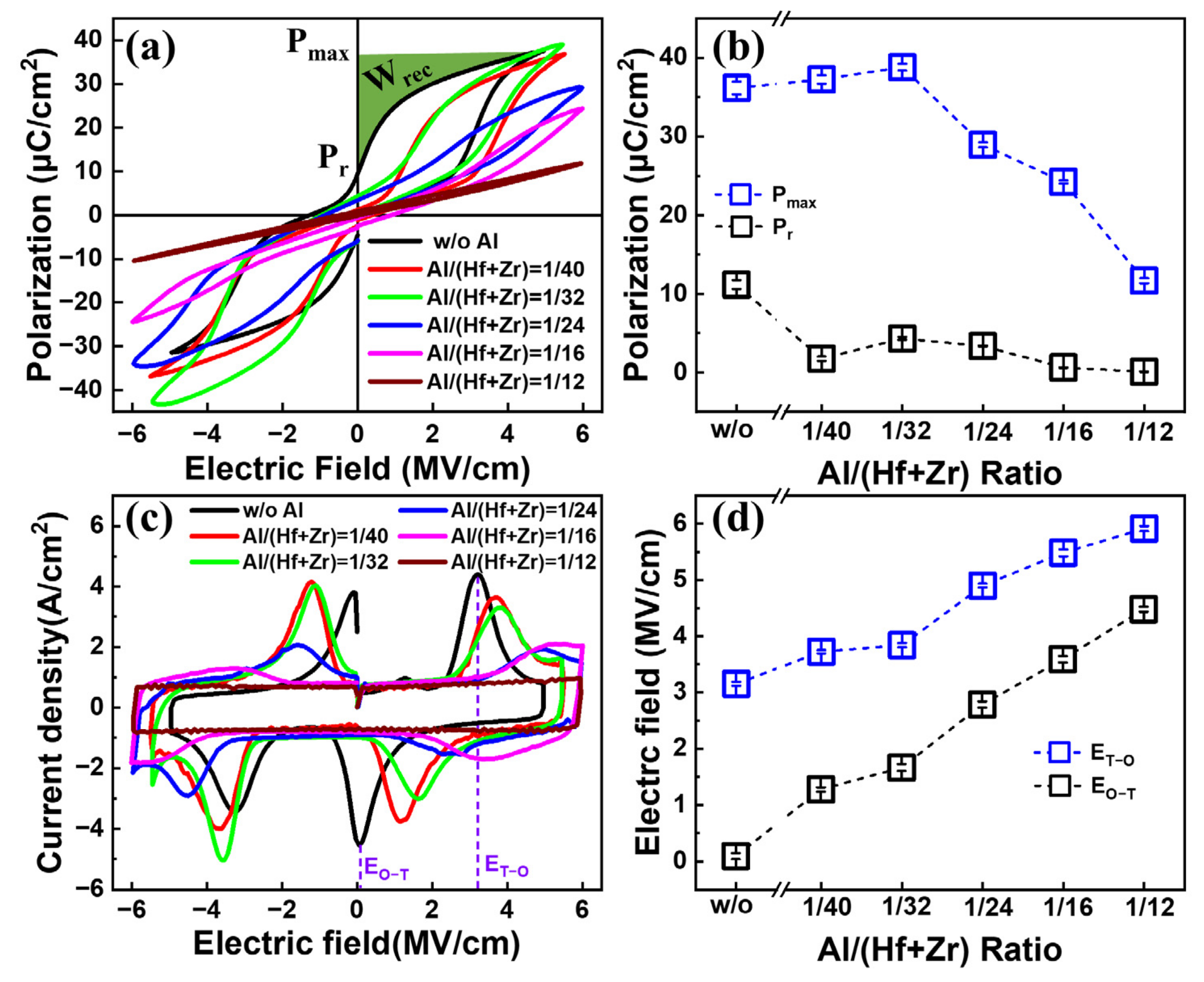
Figure 2a shows the
P–E characteristics of the fabricated capacitors with various Al/(Hf + Zr) ratios under a triangle pulse train with a frequency of 10 kHz. By increasing the Al concentration, the maximum polarization (
Pmax) and remanent polarization (
Pr) show a downward trend, accompanied by more and more pinched hysteresis loops. In detail, as shown in
Figure 2b, the
Pmax value increases slowly from 36.17 to 38.81 μC cm
−2, and then drops sharply to 11.68 μC cm
−2. Moreover, the
Pr value decreases from 11.1 to 0.04 μC cm
−2. This may be due to an increasing concentration of the T-phase in the AFE layer, which can cause a small
Pr value. The corresponding
J–E curves are shown in
Figure 2c. Four discrete peaks located in four different quadrants of the
J–E curves indicate the AFE properties of the Hf
0.5Zr
0.5O
2/HfZrO:Al nanostacks, and each current peak corresponds to a transition field (E
T-O) from the T-phase to the orthorhombic (O)-phase, or E
O-T from the O-phase to the T-phase. As the Al doping concentration increases, both E
T-O and E
O-T exhibit an increasing trend. More specifically, the E
T-O increases from 3.15 to 5.92 MV cm
−1 and the E
O-T increases from 0.1 to 4.49 MV cm
−1, as shown in
Figure 2d. However, the peak current densities show a decreasing trend. This should be ascribed to the enhanced stability of the T-phase in the Al-doped AFE thin film, leading to weak phase transitions between the T- and O-phases [
13].
Figure 3a–f depicts the C–V characteristics of the capacitors with different Al/(Hf + Zr) ratios in order to demonstrate the evolution of the capacitance density in the Hf
0.5Zr
0.5O
2/HfZrO:Al nanostacks enabled by increasing the Al doping concentration. It is found that four discrete capacitance peaks appear for the sample without Al doping, revealing the formation of antiferroelectricity [
15]. When the ratio of Al/(Hf + Zr) increases from 1/40 to 1/24, the two capacitance peaks around 0 V tend to merge into a new peak, and the maximum capacitance density is obtained near V = 0, implying an enhancement of the antiferroelectricity [
15]. However, by continuously increasing the Al concentration, the capacitance peaks vanish, and finally, the C–V curves become linear dielectric characteristics, which are consistent with the
P–E curves that become linear when the Al/(Hf + Zr) ratio increases to 1/12. This may be attributed to a change in the crystallization of the HfZrO:Al nanofilms [
6]. Therefore, it is clear that the evolution of the capacitance density is achieved by increasing the Al doping concentration.
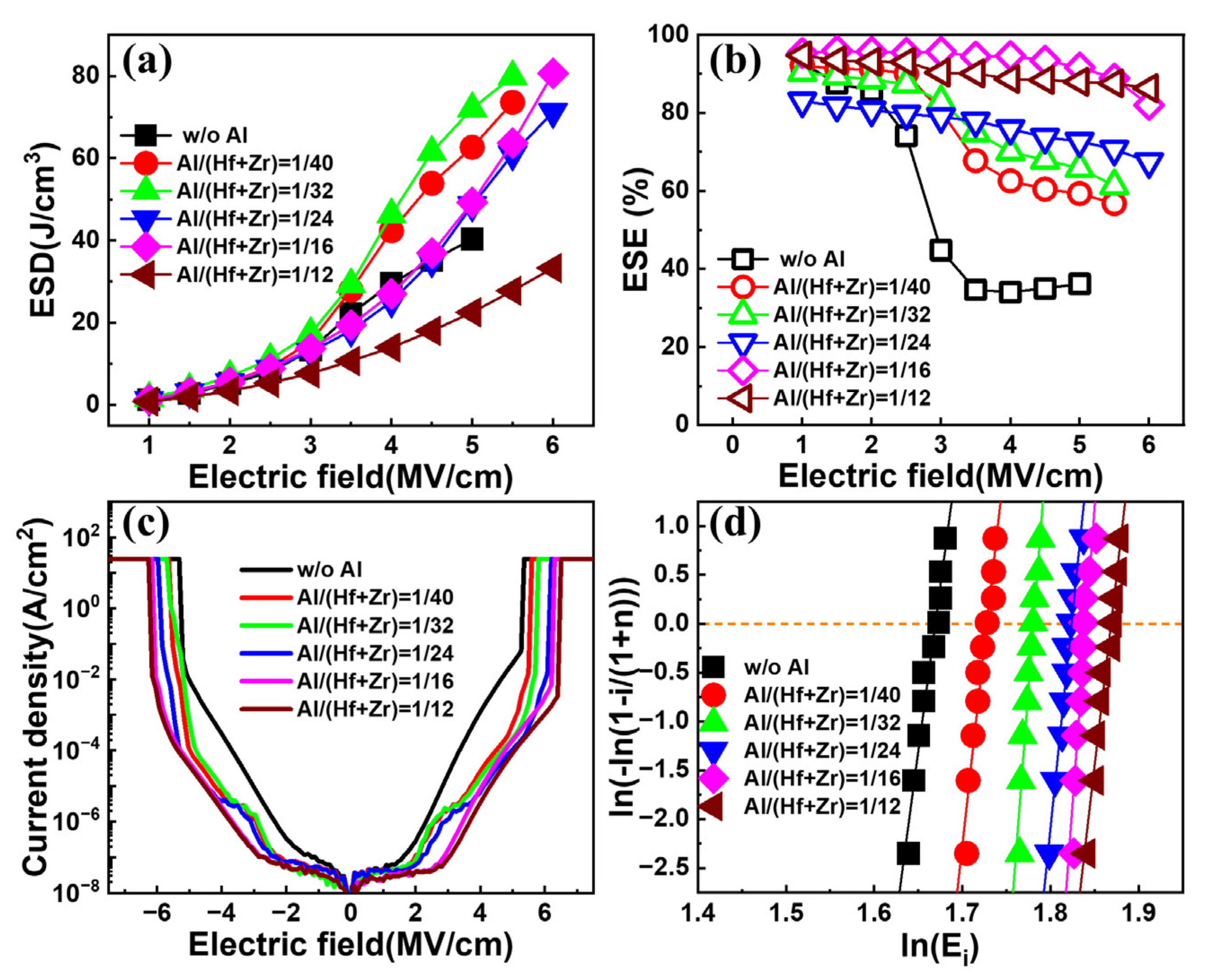
The ESD of an energy storage capacitor is usually calculated via an integral of the applied electric field (E) with respect to polarization (see a representative case in
Figure 2a), which is expressed as follows [
16].
Furthermore, the ESE can be defined as the percentage of the ESD in relation to the total stored energy density, which can be calculated according to the following formula [
16]:
Figure 4a,b show the extracted ESDs and ESEs of the fabricated capacitors with various Al/(Hf + Zr) ratios as a function of the electric field, respectively. All the capacitors exhibit an increasing ESD with the enhancing electric field. In terms of the sample without Al doping, the resulting ESD shows a gradual rise with the electric field until it reaches a near-maximum of ~40.3 J cm
−3 at 5 MV cm
−1. However, when the electric field increases slightly, the capacitor encounters an electrical breakdown. For the samples with an Al/(Hf + Zr) ratio range of 1/40~1/16, the resulting maximum ESDs are much higher than that for the undoped sample. However, when the Al/(Hf + Zr) ratio increases to 1/12, the ESD deteriorates badly. As shown in
Figure 4b, the corresponding ESE decreases gradually with the increasing electric field for all the capacitors. However, the undoped sample shows a sharp drop in the ESE when the applied electric field exceeds 2 MV cm
−1, demonstrating a very poor ESE of 36.2% at 5 MV·cm
−1. Fortunately, Al doping in the AFE layer remarkably improves the ESE, especially under high electric fields. The above results indicate that suitable Al doping in Hf
0.25Zr
0.75O
2 can obviously enhance the breakdown electric field and suppress the energy loss of the capacitor. In order to exclude that the extraction of ESDs under a high electric field are interfered by the leakage current, the I–V characteristics until the electrical breakdown are measured under DC biases. The current density–electric field curves of the capacitors with different Al/(Hf + Zr) ratios are shown in
Figure 4c, and the maximum current densities are in the range of 1~20 mA cm
−2 for the capacitors under the highest
P–E measurement electric field of 5~6 MV cm
−1. Even if the above maximum current is flown through the energy storage capacitor during the
P–E measurement within ten percent of the duration, i.e., ~10 μs, only 0.01~0.2 μC cm
−2 of the polarization would be overestimated, which is negligible compared with the
Pmax of the capacitors. The Weibull distribution of the breakdown electric field (E
B) of the capacitors with different Al/(Hf + Zr) ratios is shown in
Figure 4d. The E
B is extracted from the intersection of the fitting line and the X axis when Y = 0. Compared with the sample without Al doping, the Al-doped samples generate higher E
B. Meanwhile, the resulting E
B gradually increases with the increasing Al/(Hf + Zr) ratio of the AFE layer, i.e., from 5.63 to 6.48 MV cm
−1, which is helpful to improve the ESD.
Figure 5 shows the maximum ESDs and the corresponding ESEs of the capacitors associated with diverse Al concentrations in the AFE layer. When the ratio of Al/(Hf + Zr) is in the range of 1/40~1/16, the fabricated capacitors exhibit quite high maximum ESDs, and the highest ESD is as large as 81.4 J·cm
−3 for the Al/(Hf + Zr) ratio of 1/16. Furthermore, the corresponding ESE increases gradually up to 86.4% with increasing the ratio of Al/(Hf + Zr) to 1/12 in the AFE layer. An ideal ESE of 82.9%, corresponding to the largest ESD, is achieved at the Al/(Hf + Zr) ratio of 1/16.
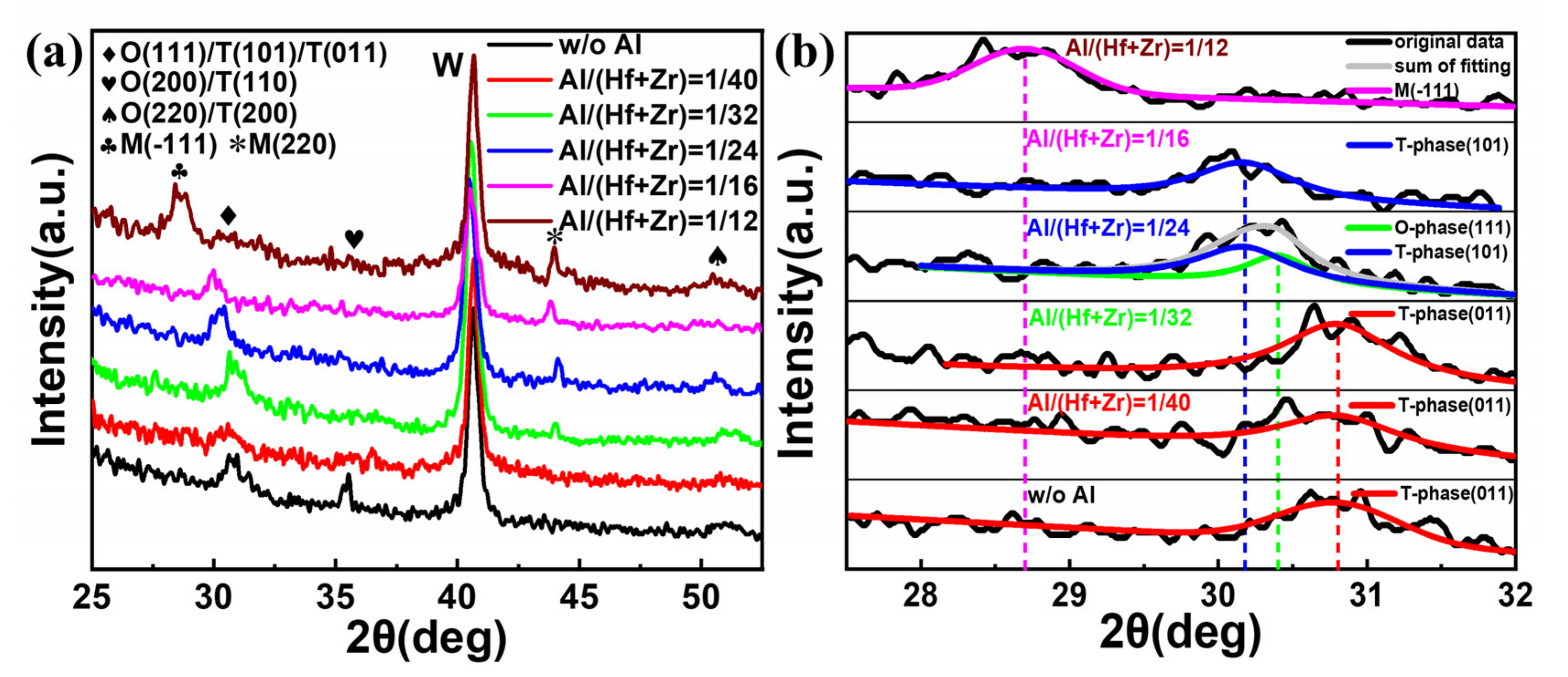
To find out the influence of the different Al/(Hf + Zr) ratios on the crystallization characteristics of the investigated dielectrics, the W top electrodes were removed using the RIE etching process after post-annealing at 450 °C for 30 min. Then, the resulting samples with W bottom electrodes and Hf
0.5Zr
0.5O
2/HfZrO:Al nanostacks were analyzed via GIXRD, and the obtained results are shown in
Figure 6a. It is clear that all the Hf
0.5Zr
0.5O
2/HfZrO:Al nanostacks with Al/(Hf + Zr) ratios from 1/40 to 1/12 as well as without Al are crystallized well, and the strong peak located at around 30°, resulting from the mixed M-, O- and T-phases in the Hf
0.5Zr
0.5O
2/HfZrO:Al nanostacks, gradually shifts from 30.8° to 28.6°. In addition, three weak diffraction peaks at 35.6°, 44.1° and 51.1° result from O- (200)/T- (110), M- (220) and O- (220)/T- (200) phases, respectively, and the strongest diffraction peak originates from the bottom W thin films [
6,
17,
18]. Moreover, the diffraction peak of O (200)/T (110) disappears and the peak of M (220) appears when the Al element is doped in the AFE layer, and the intensity of the M (220) diffraction peaks gradually increases when the Al/(Hf + Zr) ratio rises from 1/32 to 1/12. Since the diffraction peaks at 2
θ = ~30° for the Hf
1−xZr
xO
2 thin films are superimposed peaks, and the corresponding O- (111), T- (101), (011) and M- (220) phases are very close due to their structural similarities [
19,
20], the relative phases are also further analyzed to monitor the phase transition, as shown in
Figure 6b. Regarding the sample without Al doping, the resulting peak is located at 30.8°, corresponding to the T- (011) phase, and the position of the resulting peaks have no change, as the Al/(Hf + Zr) ratio rises from 1/40 to 1/32. When the Al/(Hf + Zr) ratio is 1/24, the resulting two peaks appear at 30.4° and 30.17°, which are related to the O- (111) and T- (101) phases, respectively. However, when the Al/(Hf + Zr) ratio rises to 1/16, the resulting peak is only located at 30.17°, corresponding to the T- (101) phase. When the Al/(Hf + Zr) ratio further rises to 1/12, both of the O- and T-phase disappear, and the resulting peak is located at 28.6°, corresponding to the M- (-111) phase. The aforesaid results indicate that the doping Al element in the AFE layer prevents the Hf
0.5Zr
0.5O
2/HfZrO:Al nanostacks from forming the O- (200)/T- (110) phase, and generates a new non-ferroelectric M- (220) phase. Moreover, the proportion of the M-phase gradually increases with the increasing Al/(Hf + Zr) ratio. Such an increase in the proportion of the M-phase is unfavorable to the AFE behavior, thus causing the
Pmax to decrease with the increasing Al/(Hf + Zr) ratios [
12]. In addition, the formation of the extra O- (111) phase may be responsible for the decrease in the ESD in the sample with the Al/(Hf + Zr) ratio of 1/24 due to the reduction in the relative proportion of the T-phase.
Moreover,
Table 1 compares our work with other HfO
2-based AFE capacitors [
5,
6,
7,
9,
10,
13,
14,
21,
22]. It is observed that our capacitor with the Al/(Hf + Zr) ratio of 1/16 demonstrates the highest ESD at 6 MV cm
−1 together with a perfect ESE.
In order to investigate the influence of the annealing temperature on the energy storage performance, an additional post-annealing process under various annealing temperatures is carried out for the capacitors with Al/(Hf + Zr) = 1/16.
Figure 7a shows the influence of the annealing temperature on the
P–E hysteresis loops. When the annealing temperature increases from 380 to 480 °C while fixing the annealing time of 30 min, the
Pmax value increases from 15.7 to 26.8 μC cm
−2 and the
Pr value increases from 0.36 to 4 μC cm
−2, accompanied by more and more outspread hysteresis loops. The maximum ESD and ESE of the capacitors with different annealing temperatures are shown in
Figure 7b; the obtained maximum ESD initially increases from 52.4 to 81.4 J cm
−3, and then decreases to 76.1 J cm
−3 at the annealing temperature of 480 °C. Additionally, the corresponding ESE demonstrates a decreasing tendency, reaching a value of 82.9% after annealing at 450 °C. These results indicate that 450 °C can be considered as the optimized annealing temperature for the capacitors with Al/(Hf + Zr) = 1/16. It should be noted that when the annealing temperature is ≤420 °C, it is compatible with the BEOL process. Meanwhile, the capacitors with Al/(Hf + Zr) = 1/16 still have excellent energy storage performance, and the maximum ESD and corresponding ESE are 65.7 J cm
−3 and 75%, respectively.
Further, the temperature reliabilities of our interested capacitors annealed at 450 °C are evaluated.
Figure 8a shows the typical
P–E curves at different temperatures for the Al/(Hf + Zr) ratio of 1/16. A gradual expansion of the
P–E loops can be observed as the measurement temperature increases from 25 to 225 °C, followed by a sharp expansion at 225 °C. This is because a large leakage current occurs when the temperature increases to 225 °C, as shown in the inset in
Figure 8a.
Figure 8b shows the extracted ESD and ESE at various temperatures. It is found that the maximum ESD shows a robust thermal stability until 200 °C, with a slight degradation of 2.8%. Meanwhile, the corresponding ESE also reveals a small decrease by 6.8% at 200 °C. However, the ESD and ESE decreased by 14% and 32.4% at 225 °C, respectively, which is attributed to the increased
Pr value and the outspread
P–E hysteresis loop caused by the increasing leakage current.
Figure 9a shows the typical
P–E curves for the Al/(Hf + Zr) ratio of 1/16 at various electric field cycles with a pulse field amplitude of 5~6 MV cm
−1 at 50 kHz. It is observed that no significant change can be seen for the electric field cycle-dependent
P–E curves until 10
9 cycles, when the pulse field amplitude is 5 or 5.5 MV cm
−1. When a higher pulse electric field of 6 MV cm
−1 is applied, the
P–E curve is slightly degraded after 10
8 cycles, and an increased number of pulse cycles may lead to the electrical breakdown of the device. Moreover, as shown in
Figure 9b, both the ESD and ESE exhibit negligible degeneration after 10
9 cycles at 5.5 MV cm
−1 or 10
8 cycles even at 6 MV cm
−1, demonstrating excellent electric field cycling endurance.


 ,
, 


