Abstract
Herein, titanium-dioxide-decorated organic formamidinium lead bromide perovskite thin films grown by the one-step spin-coating method are studied. TiO2 nanoparticles are widespread in FAPbBr3 thin films, which changes the optical properties of the perovskite thin films effectively. Obvious reductions in the absorption and enhancements in the intensity of the photoluminescence spectra are observed. Over 6 nm, a blueshift of the photoluminescence emission peaks is observed due to 5.0 mg/mL TiO2 nanoparticle decoration in the thin films, which originates from the variation in the grain sizes of the perovskite thin films. Light intensity redistributions in perovskite thin films are measured by using a home-built confocal microscope, and the multiple scattering and weak localization of light are analyzed based on the scattering center of TiO2 nanoparticle clusters. Furthermore, random lasing emission with sharp emission peaks is achieved in the scattering perovskite thin films with a full width at the half maximum of 2.1 nm. The multiple scattering of light, the random reflection and reabsorption of light, and the coherent interaction of light within the TiO2 nanoparticle clusters play important roles in random lasing. This work could be used to improve the efficiency of photoluminescence and random lasing emissions, and it is promising in high-performance optoelectrical devices.
1. Introduction
Halide lead perovskite thin films have been witnessed to be one of the most promising candidates in the applications of light-emitting diodes [1,2,3], photovoltaic solar cells [4,5,6], high-resolution photodetectors and displays [7,8,9], low-threshold lasers [10,11,12], and optoelectrical devices [13,14,15], owing to their high conductivity [16], long carrier diffusion lengths [17], high defect tolerances [18,19,20], and good solution processabilities [21,22,23]. Among all these APbX3 perovskite thin films, methylammonium lead tribromide (MAPbBr3), formamidinium lead tribromide (FAPbBr3), and their mixtures have attracted great attention since the certified power conversion efficiency of solar cells improved from 3.8% (MAPbBr3) to 25.7% (MAxFA1−xPbBr3) within the past few years [24,25,26,27,28,29,30]. Meanwhile, the key parameters of perovskite devices, for example the photoluminescence quantum yield (PLQY), the photoresponsivity/detectivity and external quantum efficiency (EQE) of the photodetectors, and the thresholds of vertical-cavity surface-emitting lasers (VCSEL) and random lasers (RL), showed a development trend beyond expectations, which was ascribed to the advanced high-quality thin film growth techniques, interface engineering, surface texture processing, and electron and hole transport layer materials selection [31,32,33,34,35]. Recently, good linear and nonlinear optical properties were shown in FAPbBr3 thin films, and single-photon- and multiphoton-pumped micro/nanolasers and random lasers were all explored owing to their high gain, long carrier diffusion lengths, and good bandgap tuning ability [36,37,38,39,40]. To fulfill high-Q-factor and low-threshold micro- and nanolasers in FAPbBr3 thin films, ideal nanowires, triangular, square, hexagonal, or circular micro- and nanocrystals need to be grown or fabricated, and high-performance lasers could be realized by using the total internal reflection of the boundaries [41,42,43,44,45]. Unlike the former ones, random lasers in FAPbBr3 thin films do not require an internal reflection cavity, and they are generated by the random scattering of light, the coherent interaction of light, and the stimulated radiation light amplification in irregular disordered scattering media [46,47,48,49,50]. Along this line, Xu and coworkers realized two photon-pumped random lasers in FAPbBr3/polyethylene oxide (PEO)-composited thin films with good moisture and temperature stability, where PEO worked as a coagulant to form disordered islands, and as a spacer to isolate them from the humid air outside at the same time [51]. High-efficiency up-conversion random lasing from formamidinium lead bromide/amino-mediated silica sphere composites at room temperature with a high-quality (Q) factor of 1307 and a low threshold of 413.7 µJ cm−2 was studied by Tang and coworkers [52], which originated from the multiple random scattering of light and photon recycling of the silica spheres and the high optical gain of the perovskite quantum dots. Wang and coworkers obtained low-threshold green and red random lasing emission in inorganic halide lead perovskite microcrystals with plasmonic and interferential enhancement, in which gold and silver nanoparticles and patterned sapphire substrates were used to reduce the threshold of random lasers effectively [53]. Strong scattering structures, excellent gain media, and effective coherent resonance regions played key roles in improving the random lasing action performance in FAPbBr3 thin films [54,55].
Herein, enhanced photoluminescence and random lasing emission in titanium dioxide (TiO2)-decorated organic FAPbBr3 perovskite thin films grown by using the one-step spin-coating method were studied. An obvious reduction in absorption and over 8.5 nm blueshift of the photoluminescence emission were observed along with more TiO2 nanoparticle decoration in the thin films. The reabsorption and recycling of photons and grain size changes were attributed to the photoluminescence position shift. Multiple random scattering of light and weak localization were analyzed by using a home-built confocal microscope. Low-threshold random lasing emission with sharp emission peaks in the thin films were achieved in the scattering perovskite thin films. This work is promising in developing cavity-free nanolasers and optoelectrical devices.
2. Materials and Methods
The precursor solutions of FAPbBr3 were anhydrous CH5N2Br bought from Sigma Aldrich (purity > 99.0%) and PbBr2 bought from 3A Materials (purity > 99.999%, Shanghai, China), which were dissolved in N,N-dimethylformamide (DMF, Alfa Aesar, purity > 99.8%, Shanghai, China) at a concentration ratio of 1.5:1, which was prepared in the glove box (water and oxygen component < 0.1 ppm). TiO2 rutile nanoparticle suspensions (Sigma-Aldrich, purity > 99.7%, average particle size around 25 nm, Shanghai, China) were added into the precursor solutions with concentrations of 0 mg/mL, 0.5 mg/mL, 1.0 mg/mL, 1.5 mg/mL, 2.0 mg/mL, 2.5 mg/mL, 3.0 mg/mL, 4.0 mg/mL, and 5.0 mg/mL. Then, 40 wt% FAPbBr3 solutions with TiO2 nanoparticle decoration in DMF were obtained after stirring the solution for more than 12 h by using a magnetic stirrer at room temperature. Before growing the perovskite thin films, ITO-coated glass substrates were cleaned by an ultrasonic cleaner where deionized water, acetone, ethanol, and then acetone were used, respectively. After that, the cleaned substrates were heated in a drying oven at 120 degrees to remove chemical residues and then treated with ultraviolet ozone for 15 min to improve the quality of the thin films grown by using solution-processed method. As seen in Figure 1a, Poly(3,4-ethylenedioxythiophene)/poly(styrenesulfonate) (PEDOT: PSS, 3A Materials, Shanghai, China) thin film was first coated on the cleaned ITO glass substrates by using the spin coater (4500 round/min, 60 s) to improve the morphology and quality of the active perovskite layers and annealed at 120 °C for 20 min. Finally, FAPbBr3 solutions with different concentrations of TiO2 nanoparticle decoration were grown by using the spin coater (2500 r/min, 60 s) with a thickness of around 60 nm, and the thin films were annealed at 80 °C for 20 min, as shown in Figure 1b. After completing the above operations, FAPbBr3 perovskite thin films with and without TiO2 nanoparticle decoration were prepared on the ITO glass substrate with the PEDOT:PSS buffer layer, as illustrated in Figure 1c.
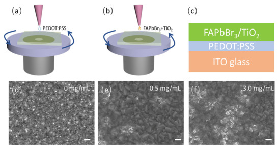
Figure 1.
(a) Schematic of the growth of PEDOT:PSS buffer layer by using one-step spin-coating method; (b) schematic of the growth of FAPbBr3(TiO2) active layer by using one-step spin-coating method; (c) the structure of the prepared FAPbBr3/TiO2 thin films on ITO-coated glass; the surface appearance of (d) FAPbBr3 thin films; (e) 0.5 mg/mL and (f) 3.0 mg/mL TiO2-nanoparticle-decorated FAPbBr3 thin films measured by using a scanning electron microscope (the scale bar is 1 µm).
3. Results and Discussion
The morphology of the FAPbBr3 perovskite thin films was analyzed by using a scanning electron microscope (SEM, JEOL JSM-7100F, Tokyo, Japan), as seen in Figure 1d,e. Without TiO2 nanoparticle decoration, the surface of the FAPbBr3 perovskite thin films is evenly and uniformly distributed. However, the surface of the FAPbBr3 perovskite thin films became more undulated, and the grain size became smaller with TiO2 nanoparticle decoration. The grain sizes might be important in the peak position and photoluminescence efficiency of the FAPbBr3 thin films. TiO2 nanoparticles disperse onto the surface of the film, and randomly distributed scattering centers are formed, spreading across the whole thin film. As the concentration of TiO2 increases, more scattering centers are obtained, which is conducive to improving the luminescence efficiency of the material and realizing low-threshold random lasing.
The granularity of the TiO2 nanoparticles and the perovskite thin films were analyzed by using a particle size analyzer (Zetasizer Nano ZS90, Malvern Panalytical Ltd., Malvern, United Kingdom). As seen in Figure 2a, the particle sizes of TiO2 nanoparticles vary from 25 nm to 27 nm, which are close to the parameters from the raw material supplier. As seen in 2b, the particle size distribution of the FAPbBr3 perovskite grains changes from 1480 nm to 294 nm, and the number of grains decreases with the increasing concentration of TiO2 nanoparticles. The optical properties of the FAPbBr3 perovskite thin films may be affected by the scattering of the grain boundaries, the reabsorption and recycling of light, and multiple scattering of light along with the varied grain sizes, which might be used to modulate the photoluminescence peak position and random lasing modes and thresholds in the FAPbBr3 perovskite thin films using TiO2 nanoparticle decoration.
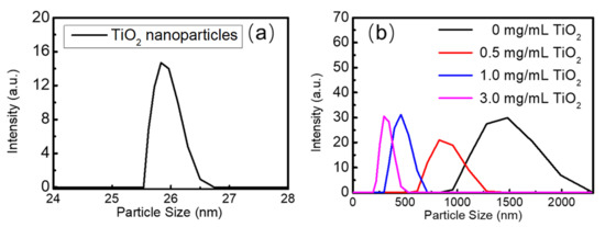
Figure 2.
(a) The particle size distribution of TiO2 nanoparticles; (b) the particle size distribution of FAPbBr3 crystals with concentrations of TiO2 at 0 mg/mL, 0.5 mg/mL, 1.0 mg/mL, and 3.0 mg/mL.
The unit structure of the FAPbBr3/TiO2 thin films was characterized by using an X-ray diffractometer (D/MAX-rB, Rigaku, Japan). As seen in Figure 3a, three prominent diffraction peaks located at 15.22°, 21.40°, and 30.26° could be seen in the X-ray diffraction spectra, which correspond to the (001), (110), and (002) peaks of the typical ABX3 perovskite structure that was determined by using the database in the JCPSD database. The room-temperature absorption spectra were measured using a UV-VIS-NIR spectrometer (Shimadzu, UV-2600, Guangzhou, China), as shown in Figure 3b. The bandgaps of the FAPbBr3 and FAPbBr3/TiO2 thin films were calculated by using the Tauc-plotted curves of the absorption spectra as 2.313 eV, 2.322 eV, 2.325 eV, 2.329 eV, and 2.330 eV, respectively, which related to the hybrid Br 4p and Pb 6s orbitals on the valence band and the Pb 6p orbitals on the conduction bands [56]. A noticeable reduction in the absorption spectra is observed above the bandgap. The photoluminescence was excited by a continuous-wave laser centered at 405 nm that was focused using a lens with a diameter of 1.0 mm, and the pumping power of the laser was set as 100 mW. The photoluminescence emission spectra were collected using an optical fiber that was connected to a spectrometer (Ocean Optics Inc., QE65Pro, Shanghai, China). As shown in Figure 3c, the photoluminescence emission spectra around 530 nm could be observed, which originate from the PbBr6 octahedra in the ABX3 perovskite structure, and are the typical spontaneous emission from the exciton recombination process [57]. The photographs of the FAPbBr3 thin films with and without TiO2 nanoparticle decoration were taken using a high-resolution camera, as seen in Figure S1 of the Supplementary Information (SI). The green photoluminescence in the FAPbBr3 without TiO2 nanoparticle decoration is relatively weak; however, it increased dramatically along with the concentration of TiO2 nanoparticles. As exhibited in Figure 3d, the intensity of photoluminescence emission increased along with the concentration of TiO2 nanoparticles until it reached 3.0 mg/mL. As high as a 16-fold enhancement of the photoluminescence emission was achieved with 3.0 mg/mL TiO2 nanoparticle decoration compared with that of the pristine FAPbBr3 membrane. A further increase in the concentration of TiO2 lead to a decrease in the fluorescent intensities, together with an 8.5 nm blueshift of the fluorescent peak. In addition, an over 8.5 nm blueshift of the photoluminescence emission peak was measured when the concentration of TiO2 nanoparticles reached 5.0 mg/mL. A gradual variation trend from 537.7 nm to 529.2 nm was observed when higher concentrations of TiO2 nanoparticles were decorated. To reduce the experimental errors and improve the reliability of the results from the optical measurement and the fiber spectrometer, the photoluminescence emission spectra of all the samples were recorded three times. The error bars for the photoluminescence intensity and peak centers were added, as shown in Figure 3d. The photoluminescence peak position could be attributed to different factors, such as the reabsorption and recycling of light, the temperature of the thin films, the grain size of the perovskite crystals, reabsorption combined with carrier diffusion, multiple scattering of light from disordered grain boundaries, and scattering centers of the TiO2 nanoparticle clusters [58]. In this work, the granularity changes in the FAPbBr3 perovskite grains play an essential role in the photoluminescence emission intensities and the emission peak centers [59]. In addition, the multiple scattering of light from the TiO2 nanoparticle clusters increases the light path thickness within the perovskite thin films, where the reabsorption and recycling of light and multiple reflections could occur. Moreover, the temperature accumulation in the thin films might also contribute to the blueshift of the photoluminescence position [60], since the temperature accumulation will intensify with more TiO2 nanoparticle clusters in the thin films.
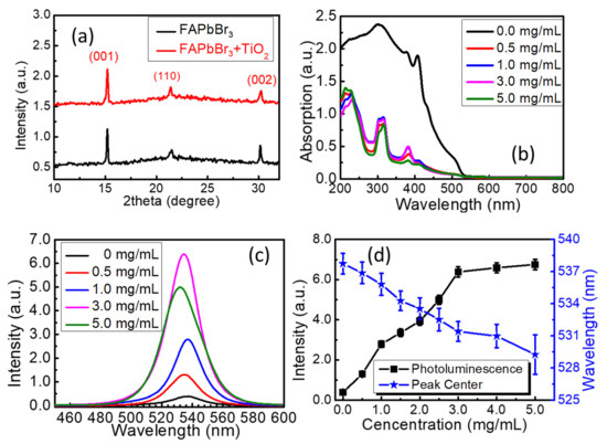
Figure 3.
(a) X-ray diffraction spectra of the FAPbBr3 and FAPbBr3/TiO2 thin films; (b) room-temperature ground-state absorption spectra of the FAPbBr3 and FAPbBr3/TiO2 thin films; (c) photoluminescence emission spectra of the FAPbBr3 and FAPbBr3/TiO2 thin films excited by a continuous-wave laser at 405 nm; (d) the photoluminescence emission intensity and wavelength versus the concentration of TiO2 nanoparticles.
To explore in-depth the photoluminescence performance of the FAPbBr3 and FAPbBr3/TiO2 thin films, excitation-power-dependent photoluminescence spectra were measured at the range of 10 mW to 130 mW with an interval of 10 mW or 20 mW, as shown in Figure 4a–c. To provide repeatable experimental results, the beam size of the excitation laser source was set to 1.0 mm in diameter, which covers hundreds of TiO2 nanoparticle clusters. The photoluminescence emissions with different concentrations of TiO2 nanoparticle decoration were collected from the whole covered areas, and each sample was measured three times. The error bars were added to illustrate the experimental differences, as shown in Figure 4d, and a good repeatability of the photoluminescence is presented. The photoluminescent intensities of FAPbBr3 thin films with and without TiO2 decoration change as the pumping powers increase, as shown in Figure 4d. The intensity of the photoluminescence emission starts to increase under the power of 30 mW in the FAPbBr3 thin films, and it reaches the maximum under the illumination power of 90 mW as the absorption is saturated by the perovskite thin films. A similar process could be observed in FAPbBr3 thin films with 1.0 mg/mL TiO2 decoration. Still, the photoluminescent intensity increases under the illumination power of 10 mW, and the absorption saturation is reached at 110 mW. The photoluminescence intensity of the latter is almost 10 times larger than the former. In sharp contrast, the photoluminescence intensity in FAPbBr3 thin films with 3.0 mg/mL TiO2 decoration exhibits another high enhancement under the pumping power of 110 mW, which is nearly 16-fold compared with that of the pristine FAPbBr3 thin films. The multiple random scattering of light caused by the TiO2 nanoparticle clusters increases the reflection possibility of light and the adequate optical thickness of the perovskite thin films, and the reabsorption and recycling of light also affect the photoluminescence efficiency and peak position. All these factors make the photoluminescence efficiency increase dramatically along with the decoration concentration of TiO2 nanoparticles.
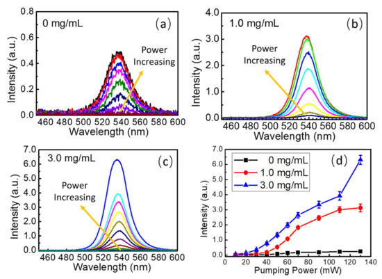
Figure 4.
(a) Photoluminescence spectra of the FAPbBr3 thin films under different pumping power; (b) photoluminescence spectra of the FAPbBr3 thin films with 1.0 mg/mL TiO2 nanoparticle decoration under different pumping power; (c) photoluminescence spectra of the FAPbBr3 thin films with 3.0 mg/mL TiO2 nanoparticle decoration under different pumping power; (d) photoluminescence intensity changes in FAPbBr3 thin films with and without TiO2 nanoparticle decoration versus pumping power.
To further study the physics behind the photoluminescence enhancement, a home-built confocal microscope was used to investigate the photoluminescence distribution at the micro-scale. As shown in Figure 5a, the white light source is collimated into a parallel beam by a lens system and passed through the beam splitter, and then the light source passes through the focusing objective lens to reach the sample surface. At the same time, another laser beam centered at 405 nm is focused on the same position through the reflection of the beam splitter to excite the fluorescence emission in the perovskite thin films. The photoluminescence emission emitted from the surface of the material returns through the reverse path to the CCD detector for imaging. As shown in Figure 5b, uniform photoluminescence with some bright spots on the grain boundaries could be observed in FAPbBr3 thin films. Figure 5c shows larger bright regions originating from multiple scatterings of light at the TiO2 nanoparticle clusters. Larger bright areas appear as the concentration of TiO2 nanoparticle is increased, as can be seen in Figure 5d. Photoluminescence distribution photographs of the FAPbBr3 thin films with concentrations of TiO2 nanoparticle decorations of 0 mg/mL, 0.5 mg/mL, 1.0 mg/mL, 1.5 mg/mL, 3.0 mg/mL, and 5.0 mg/mL were captured at a wide range using a low-magnification objective lens on the home-built fluorescence microscope, as seen in Figure S2 in SI. The photographs show the enhancement of the photoluminescence caused by the randomly distributed scattering centers and localized regions of light cross the whole thin films, and the enhancement of the photoluminescence also spreads across the whole of the thin films. Based on the photographs, the brighter photoluminescence regions originate from multiple scatterings of light and reabsorptions and recycling of light, and the photons are localized in some closed regions, which play important roles in the formation of random lasing emission, the weak localization of light, and the coherent resonance of light in the scattering media [53].
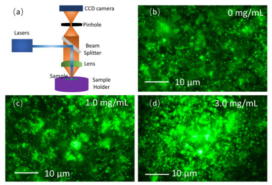
Figure 5.
(a) Schematic of the home-built confocal microscope; micro-scale photoluminescence distribution in (b) FAPbBr3 thin films, (c) FAPbBr3 thin films with 1.0 mg/mL TiO2 nanoparticle decoration, and (d) FAPbBr3 thin films with 3.0 mg/mL TiO2 nanoparticle decoration.
The scattering centers in Figure 5c,d are beneficial to the formation of cavity-free random lasers in the disordered media, where multiple scatterings and random reflections of light could take place within the FAPbBr3 thin films with TiO2 nanoparticle decoration. To study the random lasing action in TiO2-nanoparticle-decorated FAPbBr3 thin films, a nanosecond laser centered at 354.7 nm with the pulse frequency of 1.0 kHz and the pulse width of 5.0 ns was used as the excitation source and focused on the surface of the perovskite thin films with a spot diameter of 1.0 mm to cover hundreds of TiO2 nanoparticle cluster regions. As seen in Figure 6a, a broadband photoluminescence peak centered at 541.7 nm could be observed in FAPbBr3 thin films with a full width at half maximum (FWHM) of 12.8 nm, which is much narrower than that of the photoluminescence spectrum (24.2 nm). However, no random lasing emission was investigated in this thin film. With 1.0 mg/mL TiO2 nanoparticle decoration, some weak narrow peaks emerged at the right side of the photoluminescence spectrum, as seen in Figure 6b, which is the typical sign of random lasing emission. Only some stunted narrow peaks could be observed when the excitation energy surpassed 10 µJ/cm2. To improve the performance of random lasing action, sharp emission peaks with an FWHM of 2.1 nm were investigated in FAPbBr3 thin films with 3.0 mg/mL TiO2 nanoparticle decoration, as shown in Figure 6c. The intensity of the output random lasing emission and FWHM were recorded, as drawn in Figure 6d. Below the threshold, only broadband photoluminescence could be observed with an FWHM of 28 nm, which is even wider than the photoluminescence emission in Figure 6a. Above the threshold of around 5.0 µJ/cm2, the FWHM reduced to 2.1 nm rapidly, and the intensity of the sharp lasing emission increased dramatically with the excitation energy. As shown in Figure 4c,d, multiple scatterings and reflections of light from the photoluminescence occur due to the random distributed scattering centers formed by the TiO2 nanoparticle clusters and the grain boundaries of the FAPbBr3 crystals contributed to the formation of the random lasing emission. The photons are trapped in some closed regions, and the resonant interaction of light within the closed areas works as the feedback cavity of the F-P cavity lasers, and the stimulated emission of light could be occur from the scattering region when the gain surpasses the scattering and absorption loss of light. The high gain property of the FAPbBr3 perovskite thin films also plays a vital role in forming the random lasers. That is why random lasers are easier to observe in the FAPbBr3 thin films with more TiO2 nanoparticle decoration. As seen in Figure 6c, some other small peaks of random lasing emission could also be observed across the whole photoluminescence emission spectrum. These peaks originate from different localized regions of light, where the optical path is changed due to the random scattering and reflection of light across the TiO2 clusters in Figure 4d, and the reabsorption and recycling of light may also change the transport direction of light. The size of the closed region works as the cavity length of the traditional lasers, which could be used to modulate the laser modes.
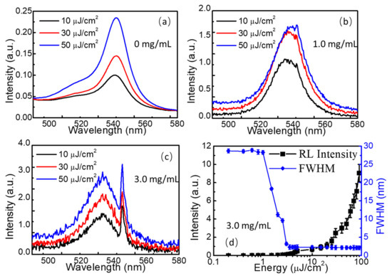
Figure 6.
(a) Photoluminescence spectra of the FAPbBr3 thin films; (b) weak narrow peaks from random lasing emission in FAPbBr3 thin films with 1.0 mg/mL TiO2 nanoparticle decoration; (c) sharp random lasing emission spectra in FAPbBr3 thin films with 3.0 mg/mL TiO2 nanoparticle decoration; (d) the intensity of the output random lasing emission and FWHM changed along with the increase in excitation energy.
The experimental results in this work provide a low-cost and easy-to-process method to enhance the photoluminescence emission and modulate the peak position of the FAPbBr3 thin films The nano- and microscale cavity-free low-threshold random lasers with an FHWM of 2.1 nm are promising for developing high-resolution light sources and displays, temperature and moisture sensors, and novel optoelectrical devices.
4. Conclusions
In conclusion, FAPbBr3 thin films without and with TiO2 nanoparticle decoration were grown by using the one-step spin-coating method. The granularity of the TiO2 nanoparticles and the perovskite thin films were analyzed by using a particle size analyzer with the particle sizes of TiO2 nanoparticles varying from 25 nm to 27 nm, and the particle size distribution of the FAPbBr3 perovskite grains changed from 1480 nm to 294 nm. An over 16-fold photoluminescence enhancement and a more than 8.5 nm blueshift of the photoluminescence emission peaks were measured, which originated from the grain size differences, the reabsorption and recycling of light, the thermal effect, and the scattering of light within the TiO2 nanoparticle clusters. The photoluminescence distribution photographs taken by the home-built confocal microscope verified the scattering contribution of the TiO2 nanoparticle clusters. Sharp random lasing emission spectra with the FHWM of 2.1 nm were detected with a low threshold of 1.0 µJ/cm2, where multiple scatterings and reflections of light, the resonant interaction of light, and the stimulated amplification of light are attributed to the formation of the random lasers. Some weak laser modes were observed that correspond to different sizes of the localized regions. This work provided a low-cost and easy-to-process method to improve the photoluminescence efficiency and achieve high-performance and low-threshold random lasers, which showed excellent application prospects in developing new light sources and high-resolution displays, sensors, and high-performance optoelectronic devices.
Supplementary Materials
The following supporting information can be downloaded at https://www.mdpi.com/article/10.3390/nano13111761/s1, Figure S1: The photographs of the FAPbBr3 thin films with and without TiO2 nanoparticles decoration. Figure S2. The distribution of photoluminescence emission in the FAPbBr3 thin films with and without TiO2 nanoparticles decoration measured by using the home-built fluorescence microscope.
Author Contributions
Conceptualization, X.L., C.X. and H.Z.; methodology, X.L. and C.X.; software, X.L.; validation, X.L., C.X. and H.Z.; formal analysis, X.L., C.X. and H.Z.; investigation, X.L., C.X., and H.Z.; resources, C.X. and H.Z.; data curation, X.L.; writing—original draft preparation, X.L.; writing—review and editing, X.L., C.X. and H.Z.; visualization, X.L., C.X. and H.Z.; supervision, C.X. and H.Z.; project administration, C.X. and H.Z.; funding acquisition, C.X. and H.Z. All authors have read and agreed to the published version of the manuscript.
Funding
This research was funded by the Project of Chongqing Talents (Grant No. CQYC202002064) and the Science and Technology Research Program of Chongqing Municipal Education Commission (Grant No. KJQN202200521).
Institutional Review Board Statement
Not applicable.
Informed Consent Statement
Not applicable.
Data Availability Statement
Not applicable.
Conflicts of Interest
The authors declare no conflict of interest.
References
- Prakasam, V.; Tordera, D.; Bolink, H.J.; Gelinck, G. Degradation mechanisms in organic lead halide perovskite light-emitting diodes. Adv. Opt. Mater. 2019, 7, 1900902. [Google Scholar] [CrossRef]
- Wei, Z.; Perumal, A.; Su, R.; Sushant, S.; Xing, J.; Zhang, Q.; Tan, S.T.; Demir, H.V.; Xiong, Q. Solution-processed highly bright and durable cesium lead halide perovskite light-emitting diodes. Nanoscale 2016, 8, 18021–18026. [Google Scholar] [CrossRef]
- Van Le, Q.; Jang, H.W.; Kim, S.Y. Recent advances toward high-efficiency halide perovskite light-emitting diodes: Review and perspective. Small Methods 2018, 2, 1700419. [Google Scholar] [CrossRef]
- Ava, T.T.; Al Mamun, A.; Marsillac, S.; Namkoong, G. A review: Thermal stability of methylammonium lead halide based perovskite solar cells. Appl. Sci. 2019, 9, 188. [Google Scholar] [CrossRef]
- Kulbak, M.; Cahen, D.; Hodes, G. How important is the organic part of lead halide perovskite photovoltaic cells? Efficient CsPbBr3 cells. J. Phys. Chem. Lett. 2015, 6, 2452–2456. [Google Scholar] [CrossRef]
- Juarez-Perez, E.J.; Wuβler, M.; Fabregat-Santiago, F.; Lakus-Wollny, K.; Mankel, E.; Mayer, T.; Jaegermann, W.; Mora-Sero, I. Role of the selective contacts in the performance of lead halide perovskite solar cells. J. Phys. Chem. Lett. 2014, 5, 680–685. [Google Scholar] [CrossRef]
- Bao, C.; Yang, J.; Bai, S.; Xu, W.; Yan, Z.; Xu, Q.; Liu, J.; Zhang, W.; Gao, F. High performance and stable all-inorganic metal halide perovskite-based photodetectors for optical communication applications. Adv. Mater. 2018, 30, 1803422. [Google Scholar] [CrossRef]
- Ray, A.; Martín-García, B.; Moliterni, A.; Casati, N.; Boopathi, K.M.; Spirito, D.; Goldoni, L.; Prato, M.; Giacobbe, C.; Giannini, C.; et al. Mixed Dimethylammonium/Methylammonium Lead Halide Perovskite Crystals for Improved Structural Stability and Enhanced Photodetection. Adv. Mater. 2022, 34, 2106160. [Google Scholar] [CrossRef]
- Tong, X.W.; Kong, W.Y.; Wang, Y.Y.; Zhu, J.M.; Luo, L.B.; Wang, Z.H. High-performance red-light photodetector based on lead-free bismuth halide perovskite film. ACS Appl. Mater. Interfaces 2017, 9, 18977–18985. [Google Scholar] [CrossRef]
- Zhang, Q.; Shang, Q.; Su, R.; Do, T.T.H.; Xiong, Q. Halide perovskite semiconductor lasers: Materials, cavity design, and low threshold. Nano Lett. 2021, 21, 1903–1914. [Google Scholar] [CrossRef]
- Hu, Z.; Liu, Z.; Zhan, Z.; Shi, T.; Du, J.; Tang, X.; Leng, Y. Advances in metal halide perovskite lasers: Synthetic strategies, morphology control, and lasing emission. Adv. Photonics 2021, 3, 034002. [Google Scholar] [CrossRef]
- Tang, B.; Dong, H.; Sun, L.; Zheng, W.; Wang, Q.; Sun, F.; Jiang, X.; Pan, A.; Zhang, L. Single-mode lasers based on cesium lead halide perovskite submicron spheres. ACS Nano 2017, 11, 10681–10688. [Google Scholar] [CrossRef] [PubMed]
- Han, T.H.; Tan, S.; Xue, J.; Meng, L.; Lee, J.W.; Yang, Y. Interface and defect engineering for metal halide perovskite optoelectronic devices. Adv. Mater. 2019, 31, 1803515. [Google Scholar] [CrossRef]
- Sun, J.; Wu, J.; Tong, X.; Lin, F.; Wang, Y.; Wang, Z.M. Organic/inorganic metal halide perovskite optoelectronic devices beyond solar cells. Adv. Sci. 2018, 5, 1700780. [Google Scholar] [CrossRef]
- Miyasaka, T. Perovskite photovoltaics: Rare functions of organo lead halide in solar cells and optoelectronic devices. Chem. Lett. 2015, 44, 720–729. [Google Scholar] [CrossRef]
- Christians, J.A.; Fung, R.C.; Kamat, P.V. An inorganic hole conductor for organo-lead halide perovskite solar cells. Improved hole conductivity with copper iodide. J. Am. Chem. Soc. 2014, 136, 758–764. [Google Scholar] [CrossRef]
- Zhumekenov, A.A.; Saidaminov, M.I.; Haque, M.A.; Alarousu, E.; Sarmah, S.P.; Murali, B.; Dursun, I.; Miao, X.H.; Abdelhady, A.L.; Wu, T.; et al. Formamidinium lead halide perovskite crystals with unprecedented long carrier dynamics and diffusion length. ACS Energy Lett. 2016, 1, 32–37. [Google Scholar] [CrossRef]
- Kang, J.; Wang, L.W. High defect tolerance in lead halide perovskite CsPbBr3. J. Phys. Chem. Lett. 2017, 8, 489–493. [Google Scholar] [CrossRef]
- Steirer, K.X.; Schulz, P.; Teeter, G.; Stevanovic, V.; Yang, M.; Zhu, K.; Berry, J.J. Defect tolerance in methylammonium lead triiodide perovskite. ACS Energy Lett. 2016, 1, 360–366. [Google Scholar] [CrossRef]
- Poindexter, J.R.; Hoye, R.L.; Nienhaus, L.; Kurchin, R.C.; Morishige, A.E.; Looney, E.E.; Osherov, A.; Correa-Baena, J.P.; Lai, B.; Bulović, V.; et al. High tolerance to iron contamination in lead halide perovskite solar cells. ACS Nano 2017, 11, 7101–7109. [Google Scholar] [CrossRef]
- Boopathi, K.M.; Karuppuswamy, P.; Singh, A.; Hanmandlu, C.; Lin, L.; Abbas, S.A.; Chang, C.C.; Wang, P.C.; Li, G.; Chu, C.W. Solution-processable antimony-based light-absorbing materials beyond lead halide perovskites. J. Mater. Chem. A 2017, 5, 20843–20850. [Google Scholar] [CrossRef]
- Leupold, N.; Panzer, F. Recent Advances and Perspectives on Powder-Based Halide Perovskite Film Processing. Adv. Funct. Mater. 2021, 31, 2007350. [Google Scholar] [CrossRef]
- Yan, F.; Tan, S.T.; Li, X.; Demir, H.V. Light generation in lead halide perovskite nanocrystals: LEDs, color converters, lasers, and other applications. Small 2019, 15, 1902079. [Google Scholar] [CrossRef] [PubMed]
- Burschka, J.; Pellet, N.; Moon, S.J.; Humphry-Baker, R.; Gao, P.; Nazeeruddin, M.K.; Grätzel, M. Sequential deposition as a route to high-performance perovskite-sensitized solar cells. Nature 2013, 499, 316–319. [Google Scholar] [CrossRef] [PubMed]
- Kojima, A.; Teshima, K.; Shirai, Y.; Miyasaka, T. Organometal halide perovskites as visible-light sensitizers for photovoltaic cells. J. Am. Chem. Soc. 2009, 131, 6050–6051. [Google Scholar] [CrossRef] [PubMed]
- Tan, Z.K.; Moghaddam, R.S.; Lai, M.L.; Docampo, P.; Higler, R.; Deschler, F.; Price, M.; Sadhanala, A.; Pazos, L.M.; Credgington, D.; et al. Bright light-emitting diodes based on organometal halide perovskite. Nat. Nanotechnol. 2014, 9, 687–692. [Google Scholar] [CrossRef]
- Chen, Q.; Wu, J.; Ou, X.; Huang, B.; Almutlaq, J.; Zhumekenov, A.A.; Guan, X.; Han, S.; Liang, L.; Yi, Z.; et al. All-inorganic perovskite nanocrystal scintillators. Nature 2018, 561, 88–93. [Google Scholar] [CrossRef]
- Saliba, M. Perovskite solar cells must come of age. Science 2018, 359, 388–389. [Google Scholar] [CrossRef]
- Wong, M.H.; An, Q.; Kress, J.; Mörsdorf, J.M.; Ballmann, J.; Vaynzof, Y. Surface dipole assisted charge carrier extraction in inverted architecture perovskite solar cells. Appl. Phys. Lett. 2021, 119, 233903. [Google Scholar] [CrossRef]
- Wu, J.; Li, X.; Lian, X.; Su, B.; Pang, J.; Li, M.D.; Xia, Z.; Zhang, J.Z.; Luo, B.; Huang, X.C. Ultrafast Study of Exciton Transfer in Sb (III)-Doped Two-Dimensional [NH3(CH2)4NH3]CdBr4 Perovskite. ACS Nano 2021, 15, 15354–15361. [Google Scholar] [CrossRef]
- Chen, P.; Meng, Y.; Ahmadi, M.; Peng, Q.; Gao, C.; Xu, L.; Shao, M.; Xiong, Z.; Hu, B. Charge-transfer versus energy-transfer in quasi-2D perovskite light-emitting diodes. Nano Energy 2018, 50, 615–622. [Google Scholar] [CrossRef]
- Meng, Y.; Ahmadi, M.; Wu, X.; Xu, T.; Xu, L.; Xiong, Z.; Chen, P. High performance and stable all-inorganic perovskite light emitting diodes by reducing luminescence quenching at PEDOT: PSS/Perovskites interface. Org. Electron. 2019, 64, 47–53. [Google Scholar] [CrossRef]
- Almond, D.P.; Bowen, C.R. An explanation of the photoinduced giant dielectric constant of lead halide perovskite solar cells. J. Phys. Chem. Lett. 2015, 6, 1736–1740. [Google Scholar] [CrossRef] [PubMed]
- Zhang, H.; Zou, C.; Chen, Y.; Wu, L.; Wen, W.; Du, B.; Feng, S.; Shang, J.; Cong, C.; Yu, T. Continuous-Wave Vertical Cavity Surface-Emitting Lasers based on Single Crystalline Lead Halide Perovskites. Adv. Opt. Mater. 2021, 9, 2001982. [Google Scholar] [CrossRef]
- Li, Y.; Zhang, X.; Huang, H.; Kershaw, S.V.; Rogach, A.L. Advances in metal halide perovskite nanocrystals: Synthetic strategies, growth mechanisms, and optoelectronic applications. Mater. Today 2020, 32, 204–221. [Google Scholar] [CrossRef]
- Wang, K.; Xing, G.; Song, Q.; Xiao, S. Micro-and nanostructured lead halide perovskites: From materials to integrations and devices. Adv. Mater. 2021, 33, 2000306. [Google Scholar] [CrossRef]
- Yuan, C.; Li, X.; Semin, S.; Feng, Y.; Rasing, T.; Xu, J. Chiral lead halide perovskite nanowires for second-order nonlinear optics. Nano Lett. 2018, 18, 5411–5417. [Google Scholar] [CrossRef]
- Ferrando, A.; Martínez Pastor, J.P.; Suárez, I. Toward metal halide perovskite nonlinear photonics. J. Phys. Chem. Lett. 2018, 9, 5612–5623. [Google Scholar] [CrossRef] [PubMed]
- Drozdowski, D.; Gągor, A.; Stefańska, D.; Zarȩba, J.K.; Fedoruk, K.; Mączka, M.; Sieradzki, A. Three-Dimensional Methylhydrazinium Lead Halide Perovskites: Structural Changes and Effects on Dielectric, Linear, and Nonlinear Optical Properties Entailed by the Halide Tuning. J. Phys. Chem. C 2022, 126, 1600–1610. [Google Scholar] [CrossRef]
- Xu, J.; Li, X.; Xiong, J.; Yuan, C.; Semin, S.; Rasing, T.; Bu, X.H. Halide perovskites for nonlinear optics. Adv. Mater. 2020, 32, 1806736. [Google Scholar] [CrossRef]
- Sun, W.; Liu, Y.; Qu, G.; Fan, Y.; Dai, W.; Wang, Y.; Song, Q.; Han, J.; Xiao, S. Lead halide perovskite vortex microlasers. Nat. Commun. 2020, 11, 4862. [Google Scholar] [CrossRef]
- Zhang, N.; Fan, Y.; Wang, K.; Gu, Z.; Wang, Y.; Ge, L.; Xiao, S.; Song, Q. All-optical control of lead halide perovskite microlasers. Nat. Commun. 2019, 10, 1770. [Google Scholar] [CrossRef]
- Wei, Q.; Li, X.; Liang, C.; Zhang, Z.; Guo, J.; Hong, G.; Xing, G.; Huang, W. Recent progress in metal halide perovskite micro-and nanolasers. Adv. Opt. Mater. 2019, 7, 1900080. [Google Scholar] [CrossRef]
- Yan, S.; Wang, K.; Xing, G.; Xu, J.; Su, S.; Tang, Z.; Wang, S.; Ng, K.W. Robust Ultralong Lead Halide Perovskite Microwire Lasers. ACS Appl. Mater. Interfaces 2021, 13, 38458–38466. [Google Scholar] [CrossRef]
- Zhu, H.; Fu, Y.; Meng, F.; Wu, X.; Gong, Z.; Ding, Q.; Gustafsson, M.V.; Trinh, M.T.; Jin, S.; Zhu, X.Y. Lead halide perovskite nanowire lasers with low lasing thresholds and high quality factors. Nat. Mater. 2015, 14, 636–642. [Google Scholar] [CrossRef]
- Dong, H.; Zhang, C.; Liu, X.; Yao, J.; Zhao, Y.S. Materials chemistry and engineering in metal halide perovskite lasers. Chem. Soc. Rev. 2020, 49, 951–982. [Google Scholar] [CrossRef]
- Kao, T.S.; Hong, Y.H.; Hong, K.B.; Lu, T.C. Perovskite random lasers: A tunable coherent light source for emerging applications. Nanotechnology 2021, 32, 282001. [Google Scholar] [CrossRef]
- Yakunin, S.; Protesescu, L.; Krieg, F.; Bodnarchuk, M.I.; Nedelcu, G.; Humer, M.; De Luca, G.; Fiebig, M.; Heiss, W.; Kovalenko, M.V. Low-threshold amplified spontaneous emission and lasing from colloidal nanocrystals of caesium lead halide perovskites. Nat. Commun. 2015, 6, 8056. [Google Scholar] [CrossRef]
- Dhanker, R.; Brigeman, A.N.; Larsen, A.V.; Stewart, R.J.; Asbury, J.B.; Giebink, N.C. Random lasing in organo-lead halide perovskite microcrystal networks. Appl. Phys. Lett. 2014, 105, 151112. [Google Scholar] [CrossRef]
- Hong, Y.H.; Kao, T.S. Room-temperature random lasing of metal-halide perovskites via morphology-controlled synthesis. Nanoscale Adv. 2020, 2, 5833–5840. [Google Scholar] [CrossRef]
- Xu, L.; Meng, Y.; Xu, C.; Chen, P. Room temperature two-photon-pumped random lasers in FAPbBr3/polyethylene oxide (PEO) composite perovskite thin film. RSC Adv. 2018, 8, 36910–36914. [Google Scholar] [CrossRef] [PubMed]
- Yang, J.; Liu, Z.; Pi, M.; Lin, H.; Zeng, F.; Bian, Y.; Shi, T.; Du, J.; Leng, Y.; Tang, X. High Efficiency Up-Conversion Random Lasing from Formamidinium Lead Bromide/Amino-Mediated Silica Spheres Composites. Adv. Opt. Mater. 2020, 8, 2000290. [Google Scholar] [CrossRef]
- Wang, J.; Chen, Q.; Xu, C.; Cao, Y.; Song, T.; Li, T.; Xu, X.; Chen, P.; Xu, L. Low-threshold green and red random lasing emission in inorganic halide lead perovskite microcrystals with plasmonic and interferential enhancement. Ceram. Int. 2023, 49, 9185–9190. [Google Scholar] [CrossRef]
- Wiersma, D.S. The physics and applications of random lasers. Nat. Phys. 2008, 4, 359–367. [Google Scholar] [CrossRef]
- Sapienza, R. Determining random lasing action. Nat. Rev. Phys. 2019, 1, 690–695. [Google Scholar] [CrossRef]
- Wang, X.; Wang, Q.; Chai, Z.; Wu, W. The thermal stability of FAPbBr3 nanocrystals from temperature-dependent photoluminescence and first-principles calculations. RSC Adv. 2020, 10, 44373–44381. [Google Scholar] [CrossRef]
- Meng, L.; Yao, E.P.; Hong, Z.; Chen, H.; Sun, P.; Yang, Z.; Li, G.; Yang, Y. Pure formamidinium-based perovskite light-emitting diodes with high efficiency and low driving voltage. Adv. Mater. 2017, 29, 1603826. [Google Scholar] [CrossRef]
- Droseros, N.; Tsokkou, D.; Banerji, N. Photophysics of Methylammonium Lead Tribromide Perovskite: Free Carriers, Excitons, and Sub-Bandgap States. Adv. Energy Mater. 2020, 10, 1903258. [Google Scholar] [CrossRef]
- Geng, X.; Liu, Y.; Zou, X.; Johansson, E.M.; Sá, J. Transient Energy-Resolved Photoluminescence Study of Excitons and Free Carriers on FAPbBr3 and FAPbBr3/SnO2 Interfaces. J. Phys. Chem. C 2023, 127, 3085–3092. [Google Scholar] [CrossRef]
- Dai, J.; Zheng, H.; Zhu, C.; Lu, J.; Xu, C. Comparative investigation on temperature-dependent photoluminescence of CH3NH3PbBr3 and CH(NH2)2PbBr3 microstructures. J. Mater. Chem. C 2016, 4, 4408–4413. [Google Scholar] [CrossRef]


Disclaimer/Publisher’s Note: The statements, opinions and data contained in all publications are solely those of the individual author(s) and contributor(s) and not of MDPI and/or the editor(s). MDPI and/or the editor(s) disclaim responsibility for any injury to people or property resulting from any ideas, methods, instructions or products referred to in the content. |
© 2023 by the authors. Licensee MDPI, Basel, Switzerland. This article is an open access article distributed under the terms and conditions of the Creative Commons Attribution (CC BY) license (https://creativecommons.org/licenses/by/4.0/).