
Optimum Contact Configurations for Quasi-One-Dimensional Phosphorene Nanodevices


Abstract
1. Introduction
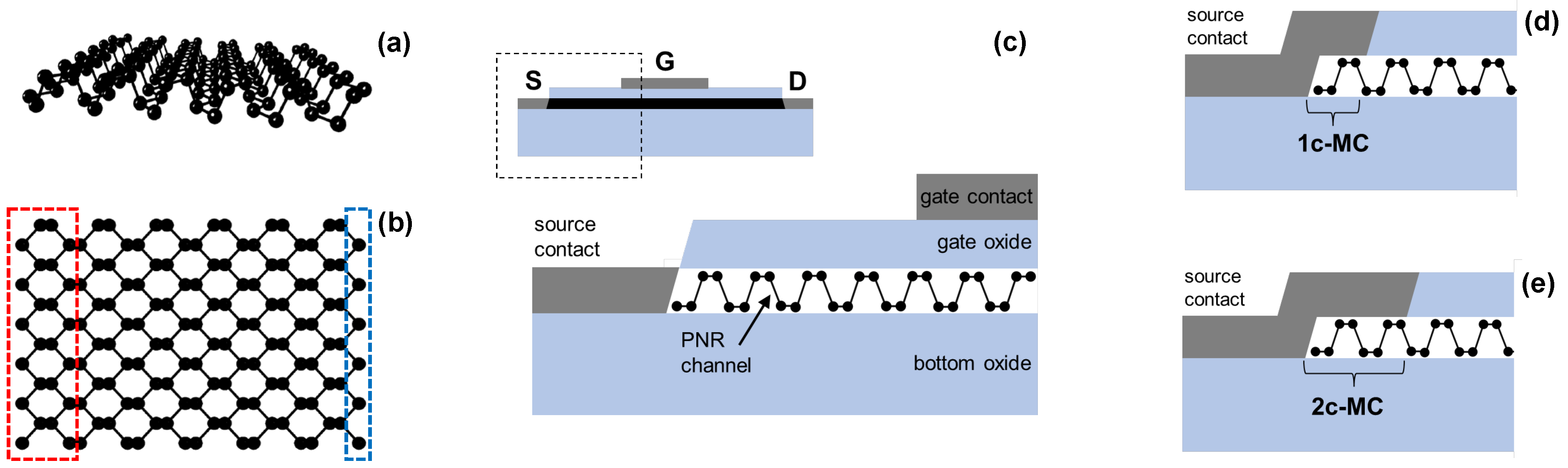
2. Methods
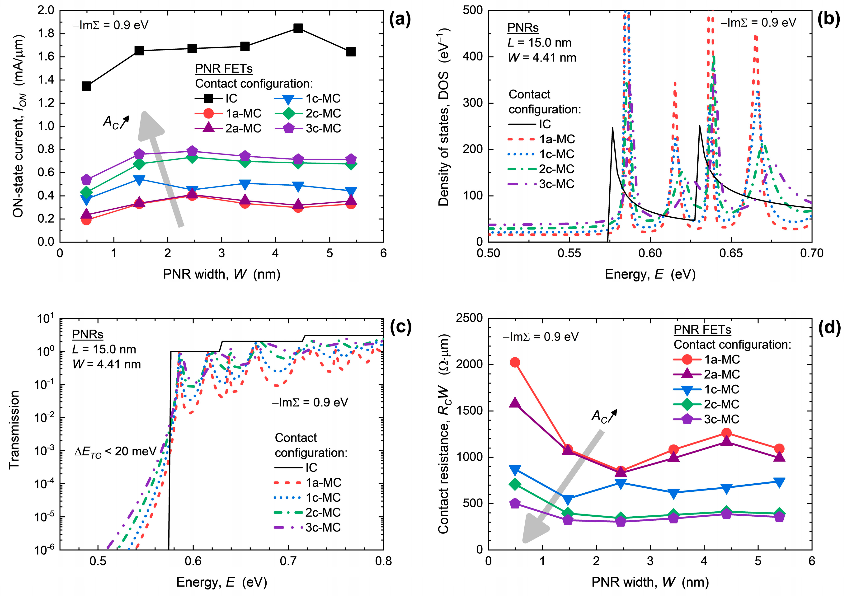
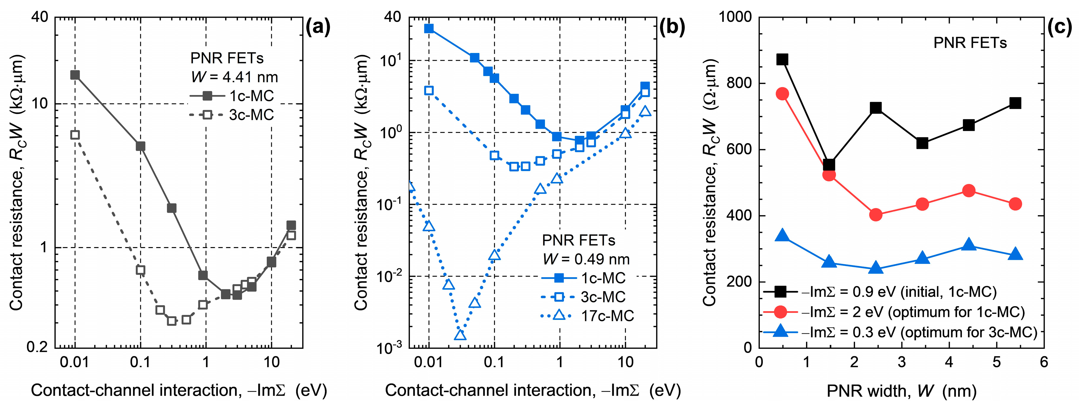
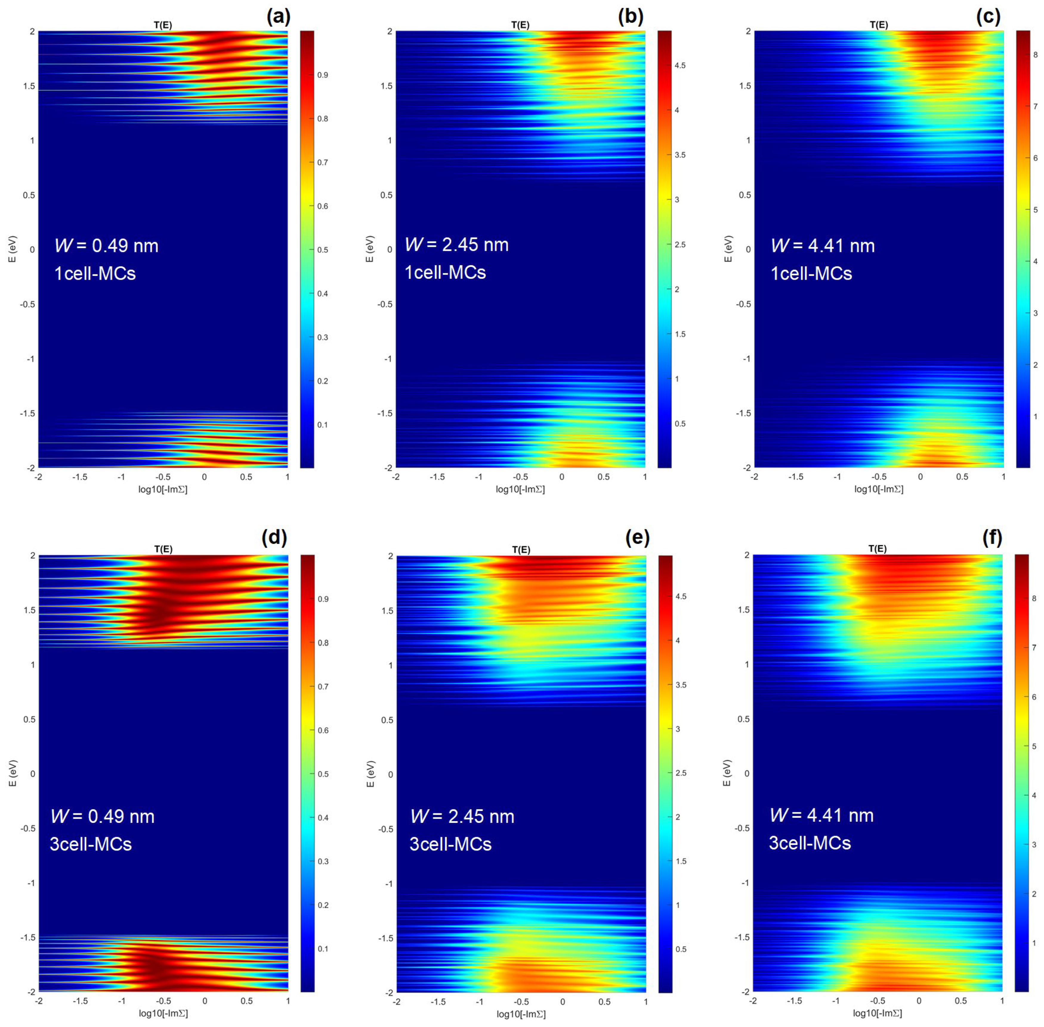
3. Results and Discussion
4. Conclusions
Supplementary Materials
Author Contributions
Funding
Data Availability Statement
Conflicts of Interest
References
- Novoselov, K.S.; Geim, A.K.; Morozov, S.V.; Jiang, D.; Zhang, Y.; Dubonos, S.V.; Grigorieva, I.V.; Firsov, A.A. Electric Field Effect in Atomically Thin Carbon Films. Science 2004, 306, 666–669. [Google Scholar] [CrossRef] [PubMed]
- Briggs, N.; Subramanian, S.; Lin, Z.; Li, X.; Zhang, X.; Zhang, K.; Xiao, K.; Geohegan, D.; Wallace, R.; Chen, L.-Q.; et al. A Roadmap for Electronic Grade 2D Materials. 2D Mater. 2019, 6, 022001. [Google Scholar] [CrossRef]
- Iannaccone, G.; Bonaccorso, F.; Colombo, L.; Fiori, G. Quantum Engineering of Transistors Based on 2D Materials Heterostructures. Nat. Nanotechnol. 2018, 13, 183–191. [Google Scholar] [CrossRef] [PubMed]
- Zeng, S.; Tang, Z.; Liu, C.; Zhou, P. Electronics Based on Two-Dimensional Materials: Status and Outlook. Nano Res. 2021, 14, 1752–1767. [Google Scholar] [CrossRef]
- Vandenberghe, W.G.; Rostami Osanloo, M. Two-Dimensional Dielectrics for Future Electronics: Hexagonal Boron Nitride, Oxyhalides, Transition-Metal Nitride Halides, and Beyond. ACS Appl. Electron. Mater. 2023, 5, 623–631. [Google Scholar] [CrossRef]
- Schwierz, F. Graphene Transistors. Nat. Nanotechnol. 2010, 5, 487–496. [Google Scholar] [CrossRef]
- Radisavljevic, B.; Radenovic, A.; Brivio, J.; Giacometti, V.; Kis, A. Single-Layer MoS2 Transistors. Nat. Nanotechnol. 2011, 6, 147–150. [Google Scholar] [CrossRef]
- Haastrup, S.; Strange, M.; Pandey, M.; Deilmann, T.; Schmidt, P.S.; Hinsche, N.F.; Gjerding, M.N.; Torelli, D.; Larsen, P.M.; Riis-Jensen, A.C.; et al. The Computational 2D Materials Database: High-Throughput Modeling and Discovery of Atomically Thin Crystals. 2D Mater. 2018, 5, 042002. [Google Scholar] [CrossRef]
- Gjerding, M.N.; Taghizadeh, A.; Rasmussen, A.; Ali, S.; Bertoldo, F.; Deilmann, T.; Knøsgaard, N.R.; Kruse, M.; Larsen, A.H.; Manti, S.; et al. Recent Progress of the Computational 2D Materials Database (C2DB). 2D Mater. 2021, 8, 044002. [Google Scholar] [CrossRef]
- Liu, H.; Neal, A.T.; Zhu, Z.; Luo, Z.; Xu, X.; Tománek, D.; Ye, P.D. Phosphorene: An Unexplored 2D Semiconductor with a High Hole Mobility. ACS Nano 2014, 8, 4033–4041. [Google Scholar] [CrossRef]
- Das, S.; Demarteau, M.; Roelofs, A. Ambipolar Phosphorene Field Effect Transistor. ACS Nano 2014, 8, 11730–11738. [Google Scholar] [CrossRef] [PubMed]
- You, H.; Jia, Y.; Wu, Z.; Wang, F.; Huang, H.; Wang, Y. Room-Temperature Pyro-Catalytic Hydrogen Generation of 2D Few-Layer Black Phosphorene under Cold-Hot Alternation. Nat. Commun. 2018, 9, 2889. [Google Scholar] [CrossRef] [PubMed]
- Miao, J.; Zhang, L.; Wang, C. Black Phosphorus Electronic and Optoelectronic Devices. 2D Mater. 2019, 6, 032003. [Google Scholar] [CrossRef]
- Chaudhary, V.; Neugebauer, P.; Mounkachi, O.; Lahbabi, S.; Fatimy, A.E. Phosphorene—An Emerging Two-Dimensional Material: Recent Advances in Synthesis, Functionalization, and Applications. 2D Mater. 2022, 9, 032001. [Google Scholar] [CrossRef]
- Li, L.; Yu, Y.; Ye, G.J.; Ge, Q.; Ou, X.; Wu, H.; Feng, D.; Chen, X.H.; Zhang, Y. Black Phosphorus Field-Effect Transistors. Nat. Nanotechnol. 2014, 9, 372–377. [Google Scholar] [CrossRef]
- Gaddemane, G.; Vandenberghe, W.G.; Van de Put, M.L.; Chen, S.; Tiwari, S.; Chen, E.; Fischetti, M.V. Theoretical Studies of Electronic Transport in Monolayer and Bilayer Phosphorene: A Critical Overview. Phys. Rev. B 2018, 98, 115416. [Google Scholar] [CrossRef]
- Szabo, A.; Rhyner, R.; Carrillo-Nunez, H.; Luisier, M. Phonon-Limited Performance of Single-Layer, Single-Gate Black Phosphorus n- and p-Type Field-Effect Transistors. In Proceedings of the IEEE International Electron Devices Meeting (IEDM), Washington, DC, USA, 7–9 December 2015; pp. 297–300. [Google Scholar]
- Watts, M.C.; Picco, L.; Russell-Pavier, F.S.; Cullen, P.L.; Miller, T.S.; Bartuś, S.P.; Payton, O.D.; Skipper, N.T.; Tileli, V.; Howard, C.A. Production of Phosphorene Nanoribbons. Nature 2019, 568, 216–220. [Google Scholar] [CrossRef]
- Zhang, W.; Enriquez, H.; Tong, Y.; Mayne, A.J.; Bendounan, A.; Smogunov, A.; Dappe, Y.J.; Kara, A.; Dujardin, G.; Oughaddou, H. Flat Epitaxial Quasi-1D Phosphorene Chains. Nat. Commun. 2021, 12, 5160. [Google Scholar] [CrossRef]
- Poljak, M.; Suligoj, T. The Potential of Phosphorene Nanoribbons as Channel Material for Ultrascaled Transistors. IEEE Trans. Electron Devices 2018, 65, 290–294. [Google Scholar] [CrossRef]
- Poljak, M.; Matić, M. Bandstructure and Size-Scaling Effects in the Performance of Monolayer Black Phosphorus Nanodevices. Materials 2022, 15, 243. [Google Scholar] [CrossRef]
- Cao, X.; Guo, J. Simulation of Phosphorene Field-Effect Transistor at the Scaling Limit. IEEE Trans. Electron Devices 2015, 62, 659–665. [Google Scholar] [CrossRef]
- Yin, D.; Yoon, Y. Design Strategy of Two-Dimensional Material Field-Effect Transistors: Engineering the Number of Layers in Phosphorene FETs. J. Appl. Phys. 2016, 119, 214312. [Google Scholar] [CrossRef]
- Liang, G.; Neophytou, N.; Lundstrom, M.S.; Nikonov, D.E. Contact Effects in Graphene Nanoribbon Transistors. Nano Lett. 2008, 8, 1819–1824. [Google Scholar] [CrossRef] [PubMed]
- Yoon, Y.; Fiori, G.; Hong, S.; Iannaccone, G.; Guo, J. Performance Comparison of Graphene Nanoribbon FETs With Schottky Contacts and Doped Reservoirs. IEEE Trans. Electron Devices 2008, 55, 2314–2323. [Google Scholar] [CrossRef]
- Poljak, M.; Matić, M. Metallization-Induced Quantum Limits of Contact Resistance in Graphene Nanoribbons with One-Dimensional Contacts. Materials 2021, 14, 3670. [Google Scholar] [CrossRef]
- Poljak, M.; Matić, M.; Župančić, T.; Zeljko, A. Lower Limits of Contact Resistance in Phosphorene Nanodevices with Edge Contacts. Nanomaterials 2022, 12, 656. [Google Scholar] [CrossRef]
- Du, Y.; Liu, H.; Deng, Y.; Ye, P.D. Device Perspective for Black Phosphorus Field-Effect Transistors: Contact Resistance, Ambipolar Behavior, and Scaling. ACS Nano 2014, 8, 10035–10042. [Google Scholar] [CrossRef]
- Haratipour, N.; Robbins, M.C.; Koester, S.J. Black Phosphorus P-MOSFETs with 7-Nm HfO2 Gate Dielectric and Low Contact Resistance. IEEE Electron Dev. Lett. 2015, 36, 411–413. [Google Scholar] [CrossRef]
- Telesio, F.; le Gal, G.; Serrano-Ruiz, M.; Prescimone, F.; Toffanin, S.; Peruzzini, M.; Heun, S. Ohmic Contact Engineering in Few–Layer Black Phosphorus: Approaching the Quantum Limit. Nanotechnology 2020, 31, 334002. [Google Scholar] [CrossRef]
- Jena, D.; Banerjee, K.; Xing, G.H. Intimate Contacts. Nat. Mater. 2014, 13, 1076–1078. [Google Scholar] [CrossRef]
- IEEE More Moore Section. International Roadmap for Devices and Systems (IRDS), 2022 Edition. Available online: https://irds.ieee.org/ (accessed on 15 February 2023).
- Poljak, M.; Song, E.B.; Wang, M.; Suligoj, T.; Wang, K.L. Influence of Edge Defects, Vacancies, and Potential Fluctuations on Transport Properties of Extremely Scaled Graphene Nanoribbons. IEEE Trans. Electron Devices 2012, 59, 3231–3238. [Google Scholar] [CrossRef]
- Poljak, M. Electron Mobility in Defective Nanoribbons of Monoelemental 2D Materials. IEEE Electron Dev. Lett. 2020, 41, 151–154. [Google Scholar] [CrossRef]
- Poljak, M.; Matić, M.; Zeljko, A. Minimum Contact Resistance in Monoelemental 2D Material Nanodevices With Edge-Contacts. IEEE Electron Dev. Lett. 2021, 42, 1240–1243. [Google Scholar] [CrossRef]
- Rudenko, A.N.; Katsnelson, M.I. Quasiparticle Band Structure and Tight-Binding Model for Single- and Bilayer Black Phosphorus. Phys. Rev. B 2014, 89, 201408. [Google Scholar] [CrossRef]
- Hu, C. Modern Semiconductor Devices for Integrated Circuits; Prentice Hall: Upper Saddle River, NJ, USA, 2010; ISBN 978-0-13-608525-6. [Google Scholar]
- Sancho, M.P.L.; Sancho, J.M.L.; Sancho, J.M.L.; Rubio, J. Highly Convergent Schemes for the Calculation of Bulk and Surface Green Functions. J. Phys. F Met. Phys. 1985, 15, 851. [Google Scholar] [CrossRef]
- Pourfath, M. The Non-Equilibrium Green’s Function Method for Nanoscale Device Simulation; Computational Microelectronics; Springer: Wien, Austria, 2014; ISBN 978-3-7091-1799-6. [Google Scholar]
- Ryndyk, D.A. Theory of Quantum Transport at Nanoscale: An Introduction; Springer Series in Solid-State Sciences; Springer International Publishing: Cham, Switzerland, 2016; ISBN 978-3-319-24086-2. [Google Scholar]
- Nemec, N.; Tománek, D.; Cuniberti, G. Modeling Extended Contacts for Nanotube and Graphene Devices. Phys. Rev. B 2008, 77, 125420. [Google Scholar] [CrossRef]
- Fediai, A.; Ryndyk, D.A.; Cuniberti, G. The Modular Approach Enables a Fully Ab Initio Simulation of the Contacts between 3D and 2D Materials. J. Phys. Condens. Matter 2016, 28, 395303. [Google Scholar] [CrossRef]
- Pan, Y.; Wang, Y.; Ye, M.; Quhe, R.; Zhong, H.; Song, Z.; Peng, X.; Yu, D.; Yang, J.; Shi, J.; et al. Monolayer Phosphorene–Metal Contacts. Chem. Mater. 2016, 28, 2100–2109. [Google Scholar] [CrossRef]
- Zhang, X.; Pan, Y.; Ye, M.; Quhe, R.; Wang, Y.; Guo, Y.; Zhang, H.; Dan, Y.; Song, Z.; Li, J.; et al. Three-Layer Phosphorene-Metal Interfaces. Nano Res. 2018, 11, 707–721. [Google Scholar] [CrossRef]
- Zhong, K.; Xu, G.; Yang, Y.; Zhang, J.-M.; Huang, Z. One- and Two-Dimensional Electrical Contacts and Transport Properties in Monolayer Black Phosphorene–Ni Interface. J. Phys. Condens. Matter 2021, 33, 145001. [Google Scholar] [CrossRef] [PubMed]
- Fediai, A.; Ryndyk, D.A.; Seifert, G.; Mothes, S.; Claus, M.; Schröter, M.; Cuniberti, G. Towards an Optimal Contact Metal for CNTFETs. Nanoscale 2016, 8, 10240–10251. [Google Scholar] [CrossRef] [PubMed]
- Li, J.; Sun, X.; Xu, C.; Zhang, X.; Pan, Y.; Ye, M.; Song, Z.; Quhe, R.; Wang, Y.; Zhang, H.; et al. Electrical Contacts in Monolayer Blue Phosphorene Devices. Nano Res. 2018, 11, 1834–1849. [Google Scholar] [CrossRef]
- Mitta, S.B.; Choi, M.S.; Nipane, A.; Ali, F.; Kim, C.; Teherani, J.T.; Hone, J.; Yoo, W.J. Electrical Characterization of 2D Materials-Based Field-Effect Transistors. 2D Mater. 2020, 8, 012002. [Google Scholar] [CrossRef]
- Szabó, Á.; Jain, A.; Parzefall, M.; Novotny, L.; Luisier, M. Electron Transport through Metal/MoS2 Interfaces: Edge- or Area-Dependent Process? Nano Lett. 2019, 19, 3641–3647. [Google Scholar] [CrossRef] [PubMed]
- English, C.D.; Shine, G.; Dorgan, V.E.; Saraswat, K.C.; Pop, E. Improved Contacts to MoS2 Transistors by Ultra-High Vacuum Metal Deposition. Nano Lett. 2016, 16, 3824–3830. [Google Scholar] [CrossRef] [PubMed]
- Cheng, Z.; Backman, J.; Zhang, H.; Abuzaid, H.; Li, G.; Yu, Y.; Cao, L.; Davydov, A.V.; Luisier, M.; Richter, C.A.; et al. Distinct Contact Scaling Effects in MoS2 Transistors Revealed with Asymmetrical Contact Measurements. Adv. Mater. 2023, 1, 2210916. [Google Scholar] [CrossRef] [PubMed]
- Afzalian, A.; Akhoundi, E.; Gaddemane, G.; Duflou, R.; Houssa, M. Advanced DFT–NEGF Transport Techniques for Novel 2-D Material and Device Exploration Including HfS2/WSe2 van Der Waals Heterojunction TFET and WTe2/WS2 Metal/Semiconductor Contact. IEEE Trans. Electron Devices 2021, 68, 5372–5379. [Google Scholar] [CrossRef]
- Matić, M.; Poljak, M. Ab Initio Quantum Transport Simulations of Monolayer GeS Nanoribbons. Solid-State Electron. 2022, 197, 108460. [Google Scholar] [CrossRef]
- Alves Machado Filho, M.; Hsiao, C.-L.; dos Santos, R.B.; Hultman, L.; Birch, J.; Gueorguiev, G.K. Self-Induced Core–Shell InAlN Nanorods: Formation and Stability Unraveled by Ab Initio Simulations. ACS Nanosci. Au 2023, 3, 84–93. [Google Scholar] [CrossRef]
- Song, S.M.; Cho, B.J. Investigation of Interaction between Graphene and Dielectrics. Nanotechnology 2010, 21, 335706. [Google Scholar] [CrossRef]
- Brahma, M.; Van de Put, M.L.; Chen, E.; Fischetti, M.V.; Vandenberghe, W.G. The Importance of the Image Forces and Dielectric Environment in Modeling Contacts to Two-Dimensional Materials. NPJ 2D Mater. Appl. 2023, 7, 14. [Google Scholar] [CrossRef]


Disclaimer/Publisher’s Note: The statements, opinions and data contained in all publications are solely those of the individual author(s) and contributor(s) and not of MDPI and/or the editor(s). MDPI and/or the editor(s) disclaim responsibility for any injury to people or property resulting from any ideas, methods, instructions or products referred to in the content. |
© 2023 by the authors. Licensee MDPI, Basel, Switzerland. This article is an open access article distributed under the terms and conditions of the Creative Commons Attribution (CC BY) license (https://creativecommons.org/licenses/by/4.0/).
Share and Cite
Poljak, M.; Matić, M. Optimum Contact Configurations for Quasi-One-Dimensional Phosphorene Nanodevices. Nanomaterials 2023, 13, 1759. https://doi.org/10.3390/nano13111759
Poljak M, Matić M. Optimum Contact Configurations for Quasi-One-Dimensional Phosphorene Nanodevices. Nanomaterials. 2023; 13(11):1759. https://doi.org/10.3390/nano13111759
Chicago/Turabian StylePoljak, Mirko, and Mislav Matić. 2023. "Optimum Contact Configurations for Quasi-One-Dimensional Phosphorene Nanodevices" Nanomaterials 13, no. 11: 1759. https://doi.org/10.3390/nano13111759
APA StylePoljak, M., & Matić, M. (2023). Optimum Contact Configurations for Quasi-One-Dimensional Phosphorene Nanodevices. Nanomaterials, 13(11), 1759. https://doi.org/10.3390/nano13111759