Article

Low-Temperature (≤500 °C) Complementary Schottky Source/Drain FinFETs for 3D Sequential Integration

1
Institute of Microelectronics, Chinese Academy of Sciences, Beijing 100029, China
2
Beijing Superstring Academy of Memory Technology, Beijing 100176, China
3
School of Microelectronics, University of Chinese Academy of Sciences, Beijing 100049, China
*
Author to whom correspondence should be addressed.
Nanomaterials 2022, 12(7), 1218; https://doi.org/10.3390/nano12071218
Submission received: 16 February 2022 / Revised: 30 March 2022 / Accepted: 1 April 2022 / Published: 5 April 2022
(This article belongs to the Special Issue Memory Nanomaterials: Growth, Characterization and Device Fabrication)

Abstract

:
In this work, low-temperature Schottky source/drain (S/D) MOSFETs are investigated as the top-tier devices for 3D sequential integration. Complementary Schottky S/D FinFETs are successfully fabricated with a maximum processing temperature of 500 °C. Through source/drain extension (SDE) engineering, competitive driving capability and switching properties are achieved in comparison to the conventional devices fabricated with a standard high-temperature (≥1000 °C) process flow. Schottky S/D PMOS exhibits an ON-state current (ION) of 76.07 μA/μm and ON-state to OFF-state current ratio (ION/IOFF) of 7 × 10⁵, and those for NMOS are 48.57 μA/μm and 1 × 10⁶. The CMOS inverter shows a voltage gain of 18V/V, a noise margin for high (NMH) of 0.17 V and for low (NML) of 0.43 V, with power consumption less than 0.9 μW at VDD of 0.8 V. Full functionality of CMOS ring oscillators (RO) are further demonstrated.

1. Introduction

The technology of 2D planar scaling is now facing major limitations, and in order to extend the semiconductor roadmap, 3D sequential integration, which consists of stacking transistors on top of each other, has been envisioned [1,2]. As its name suggests, transistor layers are processed sequentially, i.e., the top tier is processed and stacked above the already fabricated bottom tier in 3D sequential integration. This technology can enhance circuit density and functionality without the requirement of further reduction in device dimensions. To maintain the integrity of what is below, namely the bottom devices, interconnections and bonding interface, the thermal budget for top-tier fabrication is required to be no more than 550 °C [3,4,5].
However, source/drain (S/D) activation is typically performed by spike annealing at high temperature (≥1000 °C). Decreasing thermal budget will impair CMOS device performance. Much work has been undertaken to circumvent the thermal budget limitation. For instance, nanosecond laser annealing (NLA) [6] and solid-phase epitaxial regrowth (SPER) [7] were used to activate S/D as the alternatives to high-temperature spike annealing and low-temperature materials, such as poly-Si [8,9], Ge [10,11], III-V [12,13] and transparent amorphous oxide [14,15] were implemented to replace monocrystalline Si as the channel of top-tier devices. Particularly interesting is the exploration of junctionless MOSFETs as the top-tier devices with the elimination of S/D activation [16,17]. Even though impressive device performances have been achieved with such approaches, there remain several issues. NLA and SPER often incur high process cost and low throughput, and low-temperature materials are not fully compatible with current Si technology, leading to a risk of poor yield at a large scale. Additionally, junctionless devices need an extra-high-temperature (≥1000 °C) annealing to activate the channel before the top silicon layer transfer, which is likely to induce mobility degradation and threshold voltage (VTH) variation. Hence, low-temperature devices based on Si technology may be further developed.
Schottky S/D MOSFETs, using metal silicide to replace doped silicon as S/D [18], hold an inherent superiority in process thermal budget over the conventional and junctionless devices, with no need of a standard high-temperature annealing to activate S/D and channel. Therefore, in this work, low-temperature complementary Schottky S/D FinFETs are processed at a temperature as low as 500 °C, and the electrical characteristics are investigated to evaluate the feasibility of being used as the top-tier logic devices in 3D sequential technology. To our knowledge, previous investigations on Schottky S/D devices have been mostly focused on short-channel effects, with the fabrication thermal budget never lower than 600 °C [19,20,21,22,23,24]. This is the first demonstration of complementary S/D FinFETs with all process steps below 500 °C toward 3D sequential integration.

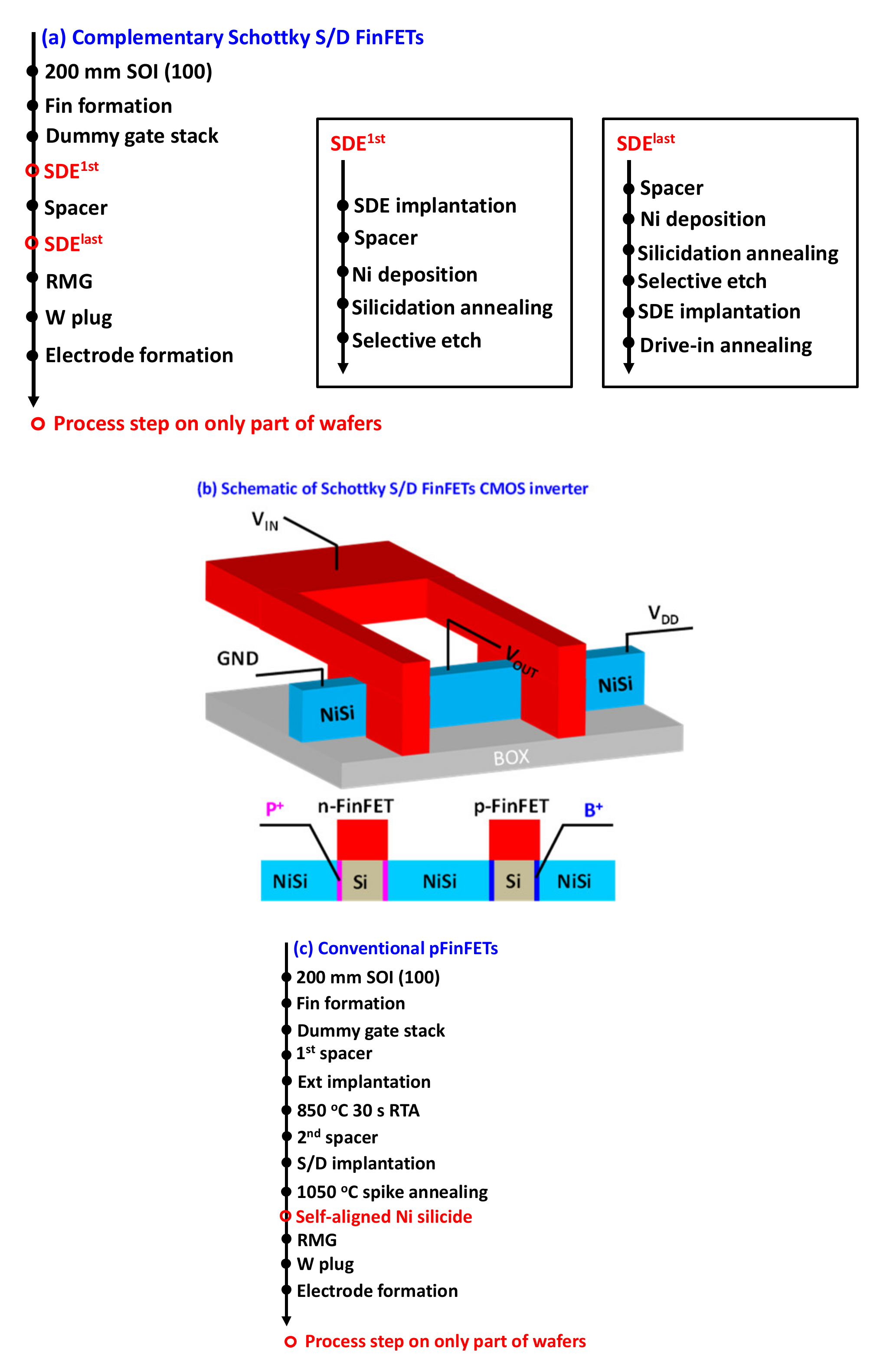
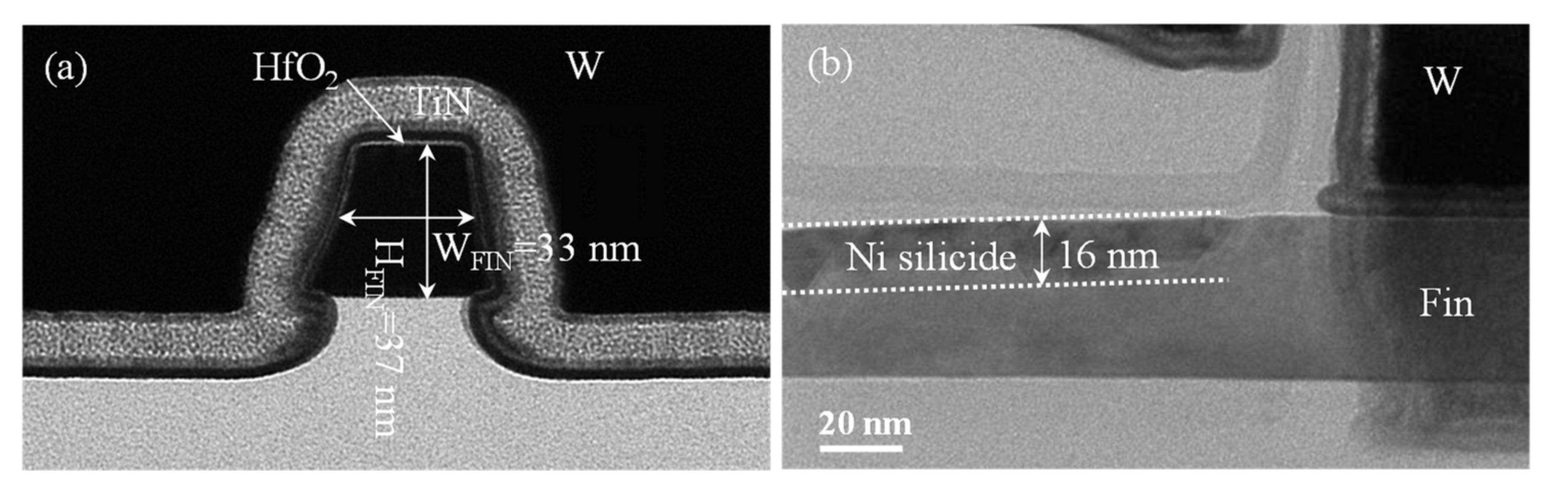
2. Device Fabrication

The process flow of Schottky S/D FinFETs is summarized in Figure 1a. SOI wafers measuring 200 mm with top Si of 40 nm and BOX of 145 nm were used as the starting materials to mimic the bonded substrate of top-tier devices. The replacement metal gate (RMG) process was adopted, and all process steps were set below the typical thermal budget of 550 °C for compatibility with 3D sequential integration [3,4,5]. According to the principle of Schottky S/D MOSFETs [18], the electrical property is primarily determined by the Schottky junction barrier between S/D and channel. In order to realize high performance, a doped source/drain extension (SDE) to lower the Schottky junction barrier, illustrated in Figure 1b, was first explored for pFinFETs by two methods, i.e., SDE first (SDE1st) and SDE last (SDElast). In the SDE1st scheme, SDE implantation was performed before the spacer and followed by silicidation annealing, and SDE was formed by dopant segregation at the silicide/Si interface during silicidation. In contrast, SDE implantation was performed after silicide formation in the SDElast scheme, and an additional rapid thermal annealing (RTA), also named drive-in annealing, was used to drive the dopant to segregate at the silicide/Si interface, forming SDE. An amount of 3 nm Ni was deposited by sputtering, and B 1.5 keV 2 × 1015 cm2 was implemented for SDE implantation in both schemes. A split, shown in Table 1, was further performed to investigate the impact of the SDE process thermal budget on device performance. Afterwards, the process flow of complementary Schottky S/D FinFETs was developed with optimal SDE engineering. Gate stacks of HfO2/TiN/TaN and HfO2/TiAl/TiN were separately applied to pFinFETs and nFinFETs for VTH adjustment. The fabrication was completed with tungsten contact plug and Al metallization. Conventional pFinFETs, with and without silicide, were also fabricated with a standard high-temperature (≥1000 °C) process flow (Figure 1c) for comparison. It is worth noting that 8-inch industrial equipment was used for the fabrication in our experiment, and the process uniformity of within wafer, wafer-to-wafer and lot-to-lot was controllable and reproducible. Current-voltage measurements (112 measurement sites for each wafer) were performed using a HP4156 parameter analyser.

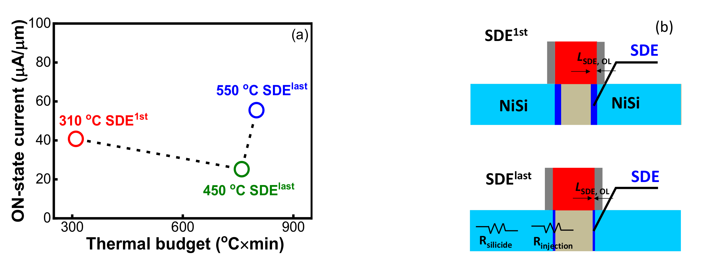
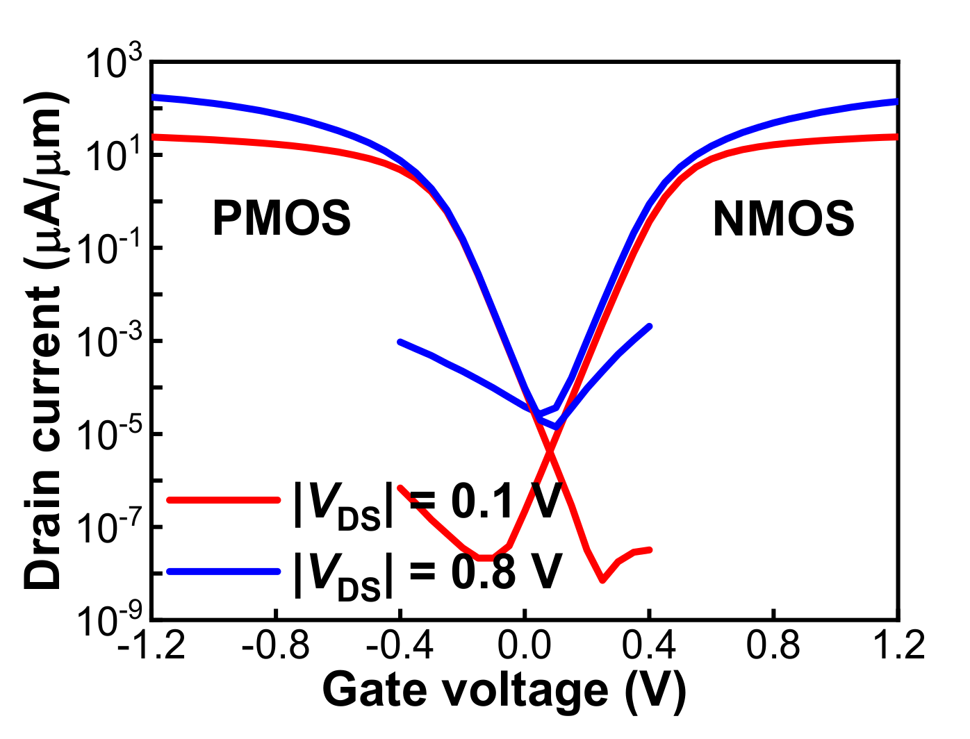
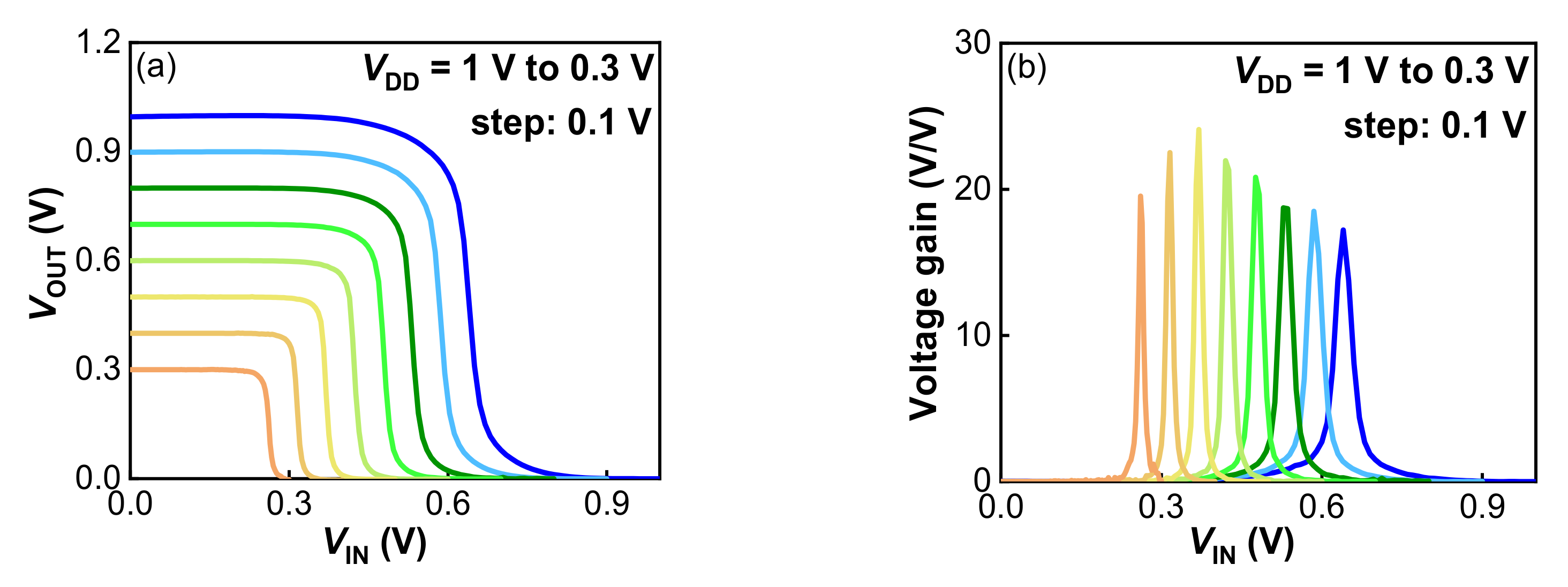
3. Results and Discussion

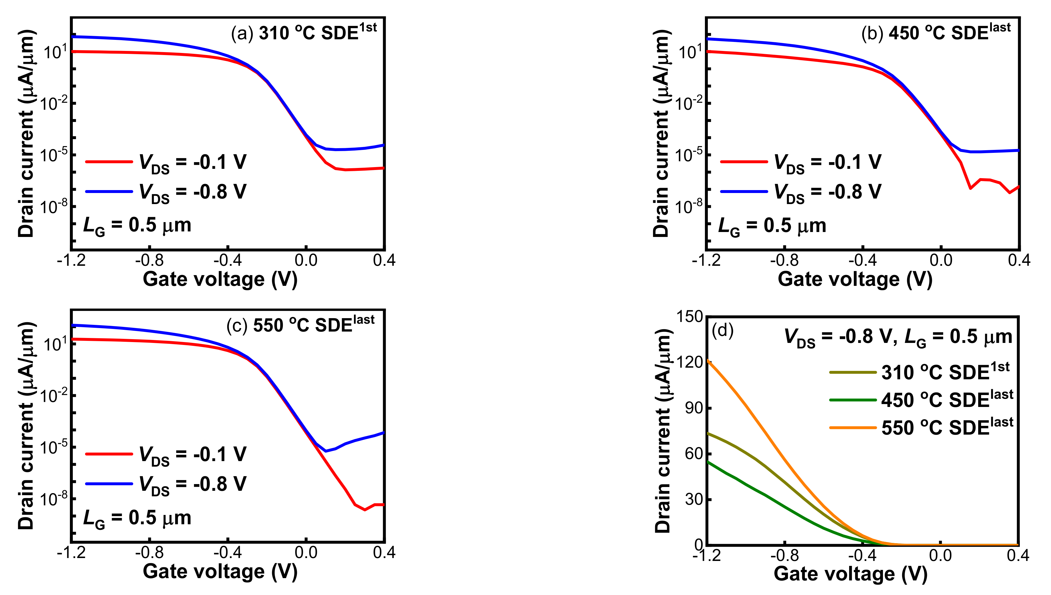
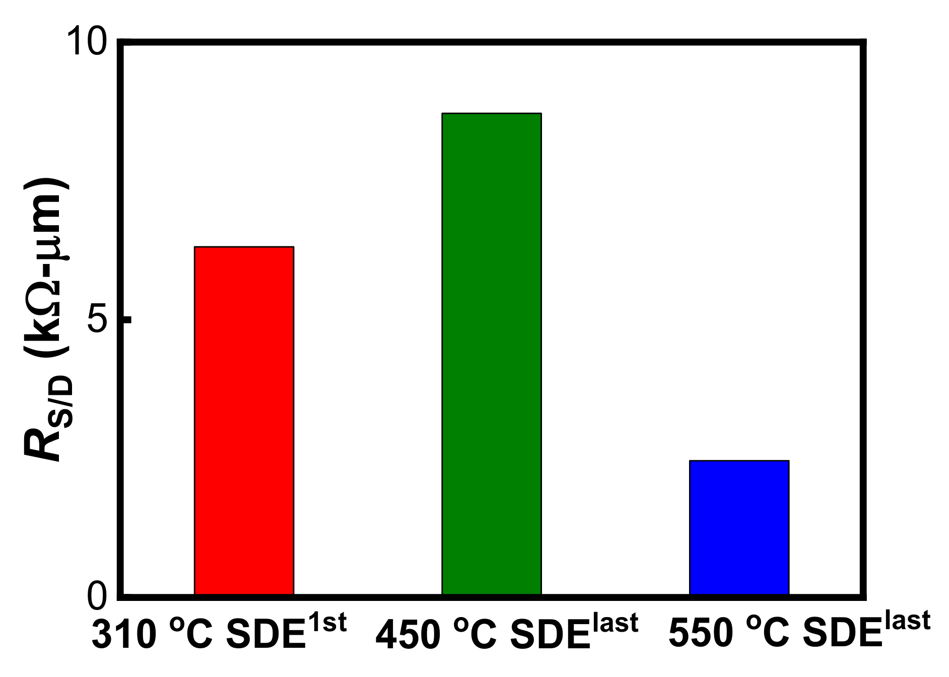
3.1. SDE Engineering

To develop the optimal SDE process, SDE engineering, shown in Table 1, was performed on pFinFETs. The IDS-VGS characteristics of the Schottky S/D pFinFETs with three SDE processes are noted in Figure 2a–c. Decent switching properties are demonstrated for all three, with ON-state to OFF-state current ratios (ION/IOFF) of 5 orders, and excellent swings (SSs) of around 61 mV/decade obtained for physical gate length (LG) of 500 nm. As compared in Figure 2d, the top ION was achieved with 550 °C SDElast, followed by 310 °C SDE1st and then 450 °C SDElast, with the values of 55.49 μA/μm, 40.78 μA/μm and 25.23 μA/μm at VDS = −0.8 V; whereas larger IOFF of 0.39 nA/μm and 0.21 nA/μm were resolved for 310 °C SDE1st and 450 °C SDElast with respect to that of 0.08 nA/μm for 550 °C SDElast. Further, the VTH defined as VGS corresponding to IDS = 10−7 A/μm were −0.13 V, −0.16 V and −0.16 V for the devices with 310 °C SDE1st, 450 °C SDElast and 550 °C SDElast processes, respectively. A reduction of around 30 mV in VTH was demonstrated for 310 °C SDE1st.
Figure 3 shows the S/D series resistance (RS/D) extracted by fitting ON-state resistance (RON) vs. 1/(VGS-VTH) at high gate bias in linear mode [25]. The RS/D measurements at VGS = −0.8 V were about 6.31 kΩ/μm, 8.71 kΩ/μm and 2.46 kΩ/μm for the devices with 310 °C SDE1st, 450 °C SDElast and 550 °C SDElast processes, respectively. Such high RS/D values are ascribed to the nano-fins scheme and to insufficiently silicided S/D, as uncovered in Figure 4. Due to the ultrathin Ni of 3 nm, about 16 nm of silicide was formed, and yet around 24 nm silicon remained unsilicided. Figure 5a further shows the ION dependence on the SDE process thermal budget, which is involved with the annealing steps in Table 1. It should be noted that the heating-up and cooling-down periods of an annealing process are ignored when defining a thermal budget. It was revealed that lowering the SDE process thermal budget degraded ION in the SDElast scheme; it seems that SDE1st prevails over SDElast in driving capability at a lower thermal budget level.
Correlating the electrical results with SDE engineering, two main findings can be made. First, SDE1st holds the advantage in ION at a lower thermal budget level, which results from the larger gate-to-SDE overlap (LSDE, OL), by performing SDE implantation before the spacer, as illustrated in Figure 5b. The reduced VTH of −0.13 V, larger IOFF of 0.39 nA/μm and lower RS/D of 6.31 kΩ/μm for 310 °C SDE1st, with reference to 450 °C SDElast, justify this point, which was performed with the same silicidation annealing. Second, in the SDElast scheme, increasing the thermal budget will lower RS/D, and thus improve ION. The lowered RS/D is probably attributable to the reductions in silicide resistance and injection resistance (Figure 5b). It is known that an Ni/Si solid state reaction forms high-resistance Ni2Si at 250–400 °C and low-resistance NiSi at 400–700 °C [26]. With the raising of silicidation annealing from 310 °C to 500 °C for 450 °C SDElast and 550 °C SDElast (Table 1), the sheet resistance of Ni silicide decreases from around 457 Ω to 123 Ω, measured with a four-point probe system. Additionally, it has been demonstrated that increasing drive-in annealing will boost dopant segregation at the silicide/Si interface, leading to an enhanced Schottky junction barrier lowering [27,28,29]. Since the injection resistance is proportional to the Schottky junction barrier, its reduction can be expected for 550 °C SDElast with respect to 450 °C SDElast, with drive-in annealing at 550 °C for the former and 450 °C for the later. One may argue that the mobility could differ with SDE process thermal budget, affecting device performance. Since no channel doping was performed for Schottky devices and all samples were tested at 300 K, it is supposed that the mobility was almost the same and the difference in IDS-VGS characteristics in Figure 2 was primarily caused by RS/D and VTH.

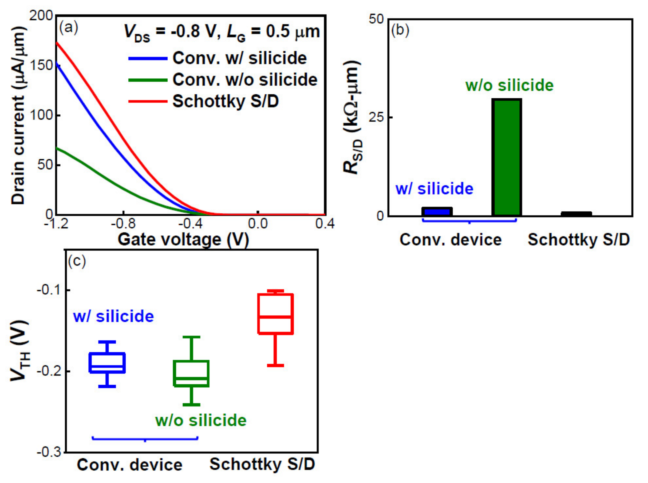
3.2. Low-Temperature Schottky S/D FinFETs vs. Conventional High-Temperature FinFETs

In accordance with the findings in Section 3.1, the fabrication of complementary Schottky S/D FinFETs with optimal SDE engineering was developed toward 3D sequential integration. The thickness of Ni was increased from 3 nm to 6 nm and 5% Pt. was added, and a two-step RTA (310 °C 60 s + selective etch + 500 °C 10 s) method was explored for silicide formation so as to avoid abnormal Ni diffusion [30,31]. Meanwhile, the drive-in annealing was further reduced from 550 °C 60 s to 500 °C 60 s for better compatibility with 3D sequential integration. Figure 6 shows the IDS-VGS characteristics of the complementary Schottky S/D FinFETs with LG = 500 nm. The ION and ION/IOFF ratios for pFinFETs were 76.07 μA/μm and 7 × 10⁵, and those for nFinFETs were 48.57 and 1 × 10⁶ μA/μm, at VDS = ±0.8 V. The corresponding VTH values were around −0.16 V and 0.3 V. Clearly, with S/D fully silicided as confirmed by XTEM images (not shown), an improvement in ION was achieved for pFinFETs due to the reduced RS/D.
A comparison was made between low-temperature Schottky S/D pFinFETs and conventional pFinFETs fabricated with a standard high-temperature (≥ 1000 °C) process flow (Figure 1c). As shown in Figure 7a, with silicide formation, the ION of conventional pFinFETs is significantly improved. Since no shift of VTH was evidenced with silicide (Figure 7c), the ION improvement is primarily attributable to the decrease in RS/D from 29 kΩ/μm to 2 kΩ/μm (Figure 7b). The low-temperature Schottky S/D pFinFETs exhibited higher ION than the conventional high-temperature devices, whether they were with (w/) or without (w/o) silicide, owing to the lower RS/D (Figure 7b) and VTH (Figure 7c). As compared to the conventional device, the Schottky S/D device using silicide as S/D holds an inherent advantage in RS/D, and its fabrication is fully compatible with current Si technology; competitive performance can be obtained with a 500 °C drive-in annealing to form SDE; moreover, no annealing at ≥1000 °C is needed to activate the channel with respect to a junctionless device [16,17]. Hence, it is indeed feasible to adopt Schottky S/D FinFETs as the top-tier devices in 3D sequential technology.

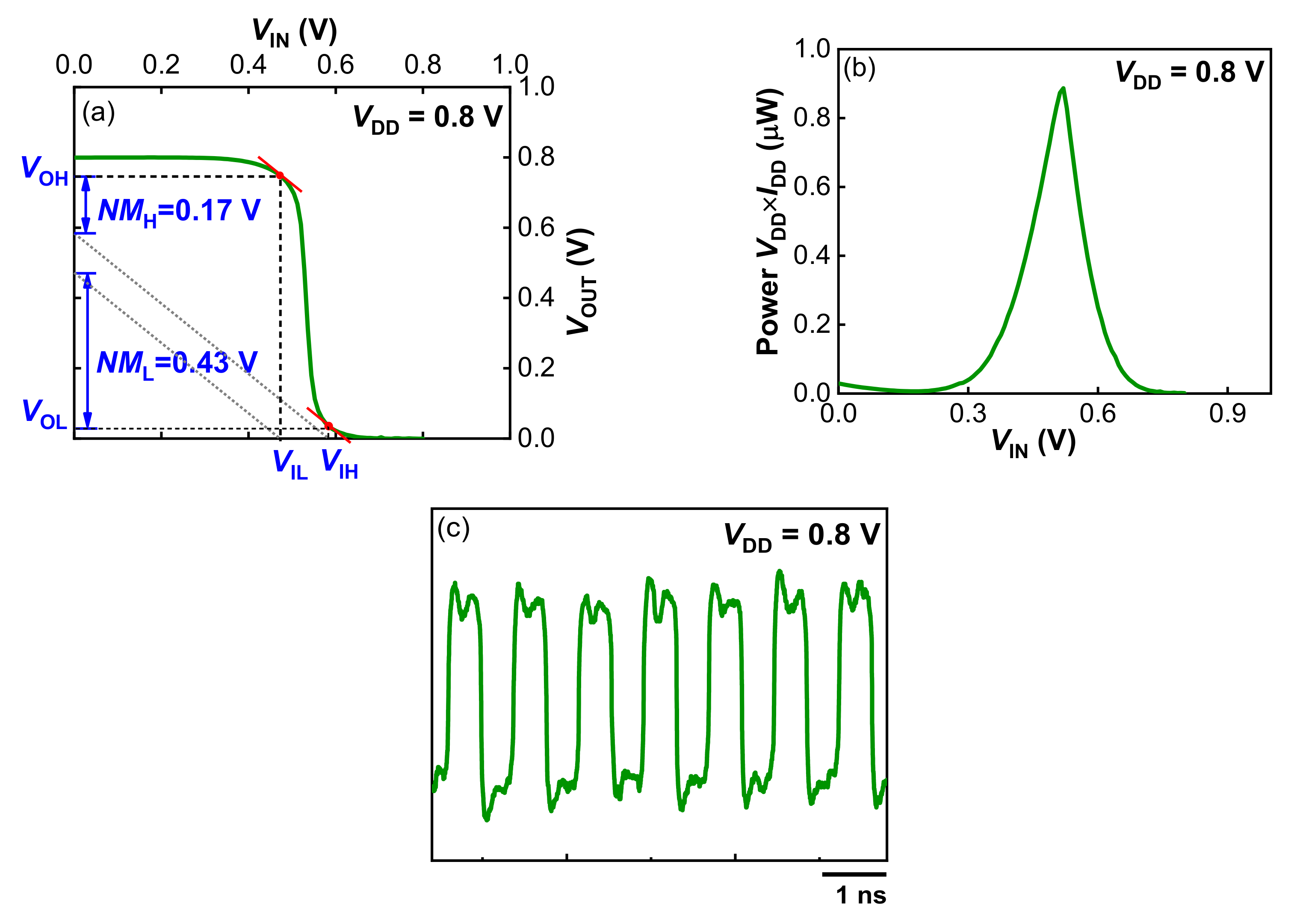
3.3. Inverter Characterization

The CMOS inverter voltage transfer characteristics (VTC) at VDD ranging from 0.3 V to 1 V by step of 0.1 V are presented in Figure 8a. The source of Schottky S/D NMOS was connected to the ground potential, while the source of Schottky S/D PMOS was attached to VDD. Both transistors shared the silicided drain contact forming the output terminal of inverter VOUT, as illustrated in Figure 1b. Well-behaved VTC was obtained, with a low-to-high output dynamic that reached rail-to-rail supply voltage range. This indicates that the subthreshold leakage currents of both transistors were sufficiently low to not degrade high and low logic states. It is noted that the transition of the inverter VTC was not located at VDD/2, due to the uncompensated asymmetry of VTH between pFinFETs and nFinFETs (Figure 6). The transition of the inverter VTC was shifted by the same amount of about 0.14 V. A gate metal work function adjustment could be applied to optimize VTH symmetry to further improve the inverter VTC. Almost a constant voltage gain (∆VOUT/∆VIN) of 18 v/v was achieved at VDD in the range of 0.3 V ~ 0.8 V (Figure 8b), suggesting a great potential of our inverter in low-power and high-performance 3D sequential integration. In order to estimate the noise margin (NM), a piecewise approximation of the VTC was used here to determine the boundary of the transition zone. As illustrated in Figure 9a, the output voltage and input voltage for high (VOH, VIH) as well as for low (VOL, VIL) were defined by the position of points where dVOUT/dVIN = −1. NM for high input (NMH = VOH − VIH) of 0.17 V and NM for low input (NML = VILVOL) of 0.43 V at VDD = 0.8 V were obtained. Figure 9b shows the static power consumption as a function of VIN at VDD = 0.8 V. The maximum static power consumption for VIN sweeping from 0 V to 0.8 V at VDD = 0.8 V was less than 0.9 μW. In Figure 9c, CMOS ring oscillators (RO) composed by 101 stages were successfully operated in low-temperature Schottky S/D FinFETs. Again, this validates the feasibility of Schottky S/D FinFETs as the top-tier devices in 3D sequential technology.

4. Conclusions

In conclusion, low-temperature complementary Schottky S/D FinFETs were proposed as the top-tier devices for 3D sequential integration and were experimentally demonstrated in this work. The thermal budget for fabrication was no more than 500 °C. and the entire process flow was fully compatible with current Si technology. With optimal SDE engineering and competitive ION values of 76.07 μA/μm and 48.57 μA/μm, ION/IOFF ratios of 7 × 10⁵ and 1 × 10⁶ at VDD = 0.8 V were obtained for pFinFETs and nFinFETs, respectively. Excellent CMOS inverter and functional CMOS RO are successfully explored, offering a new method of high-performance 3D VLSI CMOS integration.

Author Contributions

Conceptualization, methodology and writing—original draft preparation, S.M. and J.G.; methodology, validation and formal analysis, X.H., W.L., J.L. (Jinbiao Liu) and G.W.; investigation and data curation, N.Z., Y.L. (Yanna Luo) and L.C.; resources, R.Z., H.L. and X.L.; writing—review and editing, Y.L. (Yongliang Li) and Z.W.; supervision, project administration, J.L. (Junfeng Li), J.L. (Jun Luo), C.Z., W.W. and H.Y. All authors have read and agreed to the published version of the manuscript.

Funding

This work was financially supported by the Beijing National Natural Science Foundation of China under Grant No. 4222082, the Youth Innovation Promotion Association of CAS under grant No. E1YQXR006, and the National Natural Science Foundation of China under Grant No. 62004216.

Institutional Review Board Statement

Not applicable.

Informed Consent Statement

Not applicable.

Data Availability Statement

The data presented in this study are available on request from the corresponding author.

Acknowledgments

The icac core CMOS program members, the icac pilot line and testlab are acknowledged for their support.

Conflicts of Interest

The authors declare no conflict of interest.

References

  1. International Technology Roadmap for Semiconductors. Available online: http://public.itrs.net/ (accessed on 9 February 2022).
  2. Vivet, P.; Thuriès, S.; Billoint, O.; Choisnet, S.; Lattard, D.; Beigné, E.; Batude, P. Monolithic 3D: An alternative to advanced CMOS scaling, technology perspectives and associated design methodology challenges. In Proceedings of the 2018 25th IEEE International Conference on Electronics, Circuits and Systems (ICECS), Bordeaux, France, 9–12 December 2018; pp. 157–160. [Google Scholar]
  3. Lu, C.-M.; Deprat, F.; Fenouillet-Beranger, C.; Batude, P.; Garros, X.; Tsiara, A.; Leroux, C.; Gassilloud, R.; Nouguier, D.; Ney, D. Key process steps for high performance and reliable 3D Sequential Integration. In Proceedings of the 2017 Symposium on VLSI Technology, Kyoto, Japan, 5–8 June 2017; pp. T226–T227. [Google Scholar]
  4. Vandooren, A.; Witters, L.; Franco, J.; Mallik, A.; Parvais, B.; Wu, Z.; Walke, A.; Deshpande, V.; Rosseel, E.; Hikavyy, A. Sequential 3D: Key integration challenges and opportunities for advanced semiconductor scaling. In Proceedings of the 2018 International Conference on IC Design & Technology (ICICDT), Otranto, Italy, 4–6 June 2018; pp. 145–148. [Google Scholar]
  5. Fenouillet-Beranger, C.; Brunet, L.; Batude, P.; Brevard, L.; Garros, X.; Casse, M.; Lacord, J.; Sklenard, B.; Acosta-Alba, P.; Kerdiles, S. A Review of Low Temperature Process Modules Leading Up to the First (≤500 °C) Planar FDSOI CMOS Devices for 3-D Sequential Integration. IEEE Trans. Electron Devices 2021, 68, 3142–3148. [Google Scholar] [CrossRef]
  6. Vandooren, A.; Wu, Z.; Parihar, N.; Franco, J.; Parvais, B.; Matagne, P.; Debruyn, H.; Mannaert, G.; Devriendt, K.; Teugels, L. 3D sequential low temperature top tier devices using dopant activation with excimer laser anneal and strained silicon as performance boosters. In Proceedings of the 2020 IEEE Symposium on VLSI Technology, Honolulu, HI, USA, 16–19 June 2020; pp. 1–2. [Google Scholar]
  7. Micout, J.; Lapras, V.; Batude, P.; Fenouillet-Beranger, C.; Lacord, J.; Sklenard, B.; Mathieu, B.; Rafhay, Q.; Mazzocchi, V.; Colinge, J.-P. High performance low temperature FinFET with DSPER, gate last and Self Aligned Contact for 3D sequential mtegration. In Proceedings of the 2017 IEEE International Electron Devices Meeting (IEDM), San Francisco, CA, USA, 2–6 December 2017; pp. 32.32.31–32.32.34. [Google Scholar]
  8. Yang, C.-C.; Hsieh, T.-Y.; Huang, P.-T.; Chen, K.-N.; Wu, W.-C.; Chen, S.-W.; Chang, C.-H.; Shen, C.-H.; Shieh, J.-M.; Hu, C. Location-controlled-grain technique for monolithic 3D BEOL FinFET circuits. In Proceedings of the 2018 IEEE International Electron Devices Meeting (IEDM), San Francisco, CA, USA, 1–5 December 2018; pp. 11.13.11–11.13.14. [Google Scholar]
  9. Hsieh, P.-Y.; Chang, Y.-J.; Chen, P.-J.; Chen, C.-L.; Yang, C.-C.; Huang, P.-T.; Chen, Y.-J.; Shen, C.-M.; Liu, Y.-W.; Huang, C.-C. Monolithic 3D BEOL FinFET switch arrays using location-controlled-grain technique in voltage regulator with better FOM than 2D regulators. In Proceedings of the 2019 IEEE International Electron Devices Meeting (IEDM), San Francisco, CA, USA, 7–11 December 2019; pp. 3.1.1–3.1.4. [Google Scholar]
  10. Huang, C.-Y.; Dewey, G.; Mannebach, E.; Phan, A.; Morrow, P.; Rachmady, W.; Tung, I.-C.; Thomas, N.; Alaan, U.; Paul, R. 3-D self-aligned stacked NMOS-on-PMOS nanoribbon transistors for continued Moore’s law scaling. In Proceedings of the 2020 IEEE International Electron Devices Meeting (IEDM), San Francisco, CA, USA, 12–18 December 2020; pp. 20.26.21–20.26.24. [Google Scholar]
  11. Liu, Y.-W.; Hu, H.-W.; Hsieh, P.-Y.; Chung, H.-T.; Chang, S.-J.; Liu, J.-H.; Huang, P.-T.; Yang, C.-C.; Shen, C.-H.; Shieh, J.-M. Single-Crystal Islands (SCI) for Monolithic 3-D and Back-End-of-Line FinFET Circuits. IEEE Trans. Electron Devices 2021, 68, 5257–5262. [Google Scholar] [CrossRef]
  12. Deshpande, V.; Djara, V.; O’Connor, E.; Hashemi, P.; Morf, T.; Balakrishnan, K.; Caimi, D.; Sousa, M.; Fompeyrine, J.; Czornomaz, L. Three-dimensional monolithic integration of III–V and Si (Ge) FETs for hybrid CMOS and beyond. Jpn. J. Appl. Phys. 2017, 56, 04CA05. [Google Scholar] [CrossRef] [Green Version]
  13. Deshpande, V.; Djara, V.; O’Connor, E.; Hashemi, P.; Balakrishnan, K.; Sousa, M.; Caimi, D.; Olziersky, A.; Czornomaz, L.; Fompeyrine, J. Advanced 3D monolithic hybrid CMOS with sub-50 nm gate inverters featuring replacement metal gate (RMG)-InGaAs nFETs on SiGe-OI fin pFETs. In Proceedings of the 2015 IEEE International Electron Devices Meeting (IEDM), Washington, DC, USA, 7–9 December 2015; pp. 8.8.1–8.8.4. [Google Scholar]
  14. Chang, S.-W.; Lu, T.-H.; Yang, C.-Y.; Yeh, C.-J.; Huang, M.-K.; Meng, C.-F.; Chen, P.-J.; Chang, T.-H.; Chang, Y.-S.; Jhu, J.-W. First Demonstration of Heterogeneous IGZO/Si CFET Monolithic 3-D Integration With Dual Work Function Gate for Ultralow-Power SRAM and RF Applications. IEEE Trans. Electron Devices 2022, 69, 2101–2107. [Google Scholar] [CrossRef]
  15. Chakraborty, W.; Ye, H.; Grisafe, B.; Lightcap, I.; Datta, S. Low Thermal Budget (<250 °C) Dual-Gate Amorphous Indium Tungsten Oxide (IWO) Thin-Film Transistor for Monolithic 3-D Integration. IEEE Trans. Electron Devices 2020, 67, 5336–5342. [Google Scholar] [CrossRef]
  16. Vandooren, A.; Franco, J.; Parvais, B.; Wu, Z.; Witters, L.; Walke, A.; Li, W.; Peng, L.; Deshpande, V.; Bufler, F.M. 3-D sequential stacked planar devices featuring low-temperature replacement metal gate junctionless top devices with improved reliability. IEEE Trans. Electron Devices 2018, 65, 5165–5171. [Google Scholar] [CrossRef]
  17. Vandooren, A.; Franco, J.; Wu, Z.; Parvais, B.; Li, W.; Witters, L.; Walke, A.; Peng, L.; Deshpande, V.; Rassoul, N. First Demonstration of 3D stacked Finfets at a 45 nm fin pitch and 110 nm gate pitch technology on 300 mm wafers. In Proceedings of the 2018 IEEE International Electron Devices Meeting (IEDM), San Francisco, CA, USA, 1–5 December 2018; pp. 7.1.1–7.1.4. [Google Scholar]
  18. Lepselter, M.; Sze, S. SB-IGFET: An insulated-gate field-effect transistor using Schottky barrier contacts for source and drain. Proc. IEEE 1968, 56, 1400–1402. [Google Scholar] [CrossRef]
  19. Tsui, B.-Y.; Lin, C.-P. A novel 25-nm modified Schottky-barrier FinFET with high performance. IEEE Electron Device Lett. 2004, 25, 430–432. [Google Scholar] [CrossRef]
  20. Kaneko, A.; Yagishita, A.; Yahashi, K.; Kubota, T.; Omura, M.; Matsuo, K.; Mizushima, I.; Okano, K.; Kawasaki, H.; Izumida, T. High-performance FinFET with dopant-segregated Schottky source/drain. In Proceedings of the 2006 International Electron Devices Meeting, San Francisco, CA, USA, 11–13 December 2006; pp. 1–4. [Google Scholar]
  21. Khater, M.H.; Zhang, Z.; Cai, J.; Lavoie, C.; D’Emic, C.; Yang, Q.; Yang, B.; Guillorn, M.; Klaus, D.; Ott, J.A. High-k/Metal-Gate Fully Depleted SOI CMOS with Single-Silicide Schottky Source/Drain with Sub-30-nm Gate Length. IEEE Electron Device Lett. 2010, 31, 275–277. [Google Scholar] [CrossRef]
  22. Ko, C.; Chen, H.; Wang, T.; Kuan, T.; Hsu, J.; Huang, C.; Ge, C.; Lai, L.; Lee, W. NiSi Schottky barrier process-strained Si (SB-PSS) CMOS technology for high performance applications. In Proceedings of the 2006 Symposium on VLSI Technology, Honolulu, HI, USA, 13–15 June 2006; pp. 80–81. [Google Scholar]
  23. Chin, Y.; Pey, K.; Singh, N.; Lo, G.; Tan, L.; Zhu, G.; Zhou, X.; Wang, X.; Zheng, H. Excimer laser-annealed dopant segregated Schottky (ELA-DSS) Si nanowire gate-all-around (GAA) pFET with near zero effective Schottky barrier height (SBH). In Proceedings of the 2009 IEEE International Electron Devices Meeting (IEDM), San Francisco, CA, USA, 7–9 December 2009; pp. 1–4. [Google Scholar]
  24. Nishisaka, M.; Matsumoto, S.; Asano, T. Schottky source/drain SOI MOSFET with shallow doped extension. Jpn. J. Appl. Phys. 2003, 42, 2009. [Google Scholar] [CrossRef] [Green Version]
  25. Schroder, D.K. Semiconductor Material and Device Characterization; John Wiley & Sons: Hoboken, NJ, USA, 2015. [Google Scholar]
  26. Chen, L.J. Silicide Technology for Integrated Circuits; Iet: London, UK, 2004; Volume 5. [Google Scholar]
  27. Qiu, Z.; Zhang, Z.; Ostling, M.; Zhang, S.-L. A comparative study of two different schemes to dopant segregation at NiSi/Si and PtSi/Si interfaces for Schottky barrier height lowering. IEEE Trans. Electron Devices 2007, 55, 396–403. [Google Scholar] [CrossRef]
  28. Luo, J.; Qiu, Z.-J.; Zhang, Z.; Östling, M.; Zhang, S.-L. Interaction of NiSi with dopants for metallic source/drain applications. J. Vac. Sci. Technol. B Nanotechnol. Microelectron. Mater. Processing Meas. Phenom. 2010, 28, C1I1–C1I11. [Google Scholar] [CrossRef]
  29. Zhang, Z.; Qiu, Z.; Liu, R.; Ostling, M.; Zhang, S.-L. Schottky-barrier height tuning by means of ion implantation into preformed silicide films followed by drive-in anneal. IEEE Electron Device Lett. 2007, 28, 565–568. [Google Scholar] [CrossRef]
  30. Lu, J.; Miles, D.; Zhao, J.; Gurba, A.; Xu, Y.; Lin, C.; Hewson, M.; Ruan, J.; Tsung, L.; Kuan, R. A novel nickel SALICIDE process technology for CMOS devices with sub-40 nm physical gate length. In Proceedings of the Digest. International Electron Devices Meeting, San Francisco, CA, USA, 8–11 December 2002; pp. 371–374. [Google Scholar]
  31. Kim, J.; Park, T.; Lee, S.; Lee, S.; Kim, C.; Hyun, S.; Kim, Y.; Hwang, K.; Kim, H. Effect of Millisecond Annealing Temperature of Ni 1-x Pt. x Si Formation on Leakage Current Characteristics of Static Random-Access Memory Cells. IEEE Trans. Electron Devices 2018, 66, 389–394. [Google Scholar] [CrossRef]
Figure 1. (a) Process flow of Schottky S/D FinFETs in this work, (b) Schematic layout and cross section of the complementary Schottky S/D FinFETs inverter, (c) Standard high-temperature process flow of conventional device.
Nanomaterials 12 01218 g001
Figure 2. IDS-VGS characteristics of the Schottky S/D pFinFETs with (a) 310 °C SDE1st, (b) 450 °C SDElast and (c) 550 °C SDElast processes; (d) Comparison of IDS at VDS = −0.8 V between the three.
Nanomaterials 12 01218 g002
Figure 3. RS/D at VDS = −0.1 V of the Schottky S/D pFinFETs with different SDE processes.
Nanomaterials 12 01218 g003
Figure 4. Cross-sectional transmission electron microscope (XTEM) images of the Schottky S/D pFinFETs (a) across and (b) along fins with gate stack covering, fabricated with 550 °C SEDlast process.
Nanomaterials 12 01218 g004
Figure 5. (a) ION dependence on SDE process thermal budget for Schottky S/D pFinFETs, (b) Schematic of gate-to-SDE overlap (LSDE, OL) and RS/D component for the devices with SDE1st and SDElast processes.
Nanomaterials 12 01218 g005
Figure 6. IDS-VGS characteristics of low-temperature complementary Schottky S/D FinFETs with LG = 500 nm.
Nanomaterials 12 01218 g006
Figure 7. Comparison of (a) IDS at VDS = −0.8 V, (b) RS/D and (c) VTH between low-temperature Schottky S/D device and conventional (conv.) high-temperature device.
Nanomaterials 12 01218 g007
Figure 8. (a) Inverter VTC at VDD ranging from 1 V down to 0.3 V, (b) Corresponding voltage gains.
Nanomaterials 12 01218 g008
Figure 9. (a) Linear approximation of the VTC to estimate the static NMs, (b) Static power consumption with respect to VIN, (c) Characteristics of 101-stage CMOS RO based on low-temperature Schottky S/D FinFETs.
Nanomaterials 12 01218 g009
Table 1. Split of thermal budget for SDE formation.
Item 1310 °C SDE 1st450 °C SDE last550 °C SDE last
Silicidation annealing310 °C 60 s310 °C 60 s500 °C 30 s
Drive-in annealingNA450 °C 60 s550 °C 60 s
1 All annealing steps were performed by RTA.
Publisher’s Note: MDPI stays neutral with regard to jurisdictional claims in published maps and institutional affiliations.

