Review

Recent Advances in Synthesis and Application of Metal Oxide Nanostructures in Chemical Sensors and Biosensors

by
Vincentas Maciulis
1,2,
Almira Ramanaviciene
2,* and
Ieva Plikusiene
1,2,*
1
State Research Institute Centre for Physical Sciences and Technology, Sauletekio Ave. 3, LT-10257 Vilnius, Lithuania
2
Nanotechnas–Center of Nanotechnology and Materials Science, Faculty of Chemistry and Geosciences, Vilnius University, Naugarduko Str. 24, LT-03225 Vilnius, Lithuania
*
Authors to whom correspondence should be addressed.
Nanomaterials 2022, 12(24), 4413; https://doi.org/10.3390/nano12244413
Submission received: 22 November 2022 / Revised: 6 December 2022 / Accepted: 7 December 2022 / Published: 10 December 2022
(This article belongs to the Special Issue Synthesis and Application of Optical Nanomaterials)

Abstract

:
Nanostructured materials formed from metal oxides offer a number of advantages, such as large surface area, improved mechanical and other physical properties, as well as adjustable electronic properties that are important in the development and application of chemical sensors and biosensor design. Nanostructures are classified using the dimensions of the nanostructure itself and their components. In this review, various types of nanostructures classified as 0D, 1D, 2D, and 3D that were successfully applied in chemical sensors and biosensors, and formed from metal oxides using different synthesis methods, are discussed. In particular, significant attention is paid to detailed analysis and future prospects of the synthesis methods of metal oxide nanostructures and their integration in chemical sensors and biosensor design.

Graphical Abstract

1. Introduction

Nanostructured materials offer a number of advantages, such as large surface area, improved mechanical and other physical properties, as well as adjustable electronic properties that are important in the development of various sensors [1,2,3,4,5,6,7,8]. Properties of nanostructures differ greatly when compared to bulk materials. New material properties appear at nanometer dimensions, and a greater amount of atoms are found on the surface of the nanoparticle compared to higher volume particles. Therefore, the size is inversely proportional to the surface area and its surface-to-volume ratio [9]. Nanostructures are classified using the dimensions of the nanostructure itself and their components. Nanostructure classes were built using the comprising elementary units, namely, 0D nanoclusters and nanoparticles, 1D nanotubes and nanowires, and 2D nanoplates and nanolayers [10]. Nanostructures where the particles are smaller than 100 nm in all relevant directions can be referred to as ‘0D nanostructures’. These nanostructures include nanoclusters, nanospheres and fluorescent semiconductor nanocrystals—quantum dots [11,12,13]. For example, ZnO nanospheres can be prepared from zinc acetate in an alcoholic solution under basic conditions; however, the shape of the particles is very sensitive to the concentration of precursor materials [14]. Therefore, to allow some nanoparticle size control and protection from aggregation, 0D nanostructures must be synthesized from micelles or within hard templates. One avenue for the formation of 0D nanostructures is the use of soft templates, surfactants, or polymers of well-defined structure, dendrimers. Alternatively, surface masking or patterning can also be used, applying different lithographic approaches [15]. One-dimensional nanostructures are structures that have lateral dimensions greater than 100 nm, which can be formed using different metals and metal oxides and obtain desirable morphology, such as nanowires, nanorods, nanotubes, nanobelts, and nanoribbons [16,17,18,19]. Because of their unique properties and potential in application for many fields such as batteries, solar cells, gas sensors and biosensing, these materials are being studied in great detail [20,21,22]. Various synthesis approaches are available for the formation of 1D nanostructures, electrospinning, electrochemical deposition/anodization, chemical/physical vapor deposition, and chemical bath deposition [23]. Two-dimensional nanostructures are two-dimensional structures, such as nanofilms, nanocoatings, nanolayers, and nanowalls. All of these structures have a large surface-to-volume ratio and confined thickness, which is highly desirable in applications such as catalysis, photovoltaics, and sensing [24,25,26,27]. Example methods to synthesize 2D materials include: liquid exfoliation, chemical vapor deposition (CVD), and atomic layer deposition (ALD) [28]. The nanostructures named ‘3D nanostructures’ are made of lower dimensional structures (0D, 1D, 2D); thus, the 3D nanostructures have the most varied morphology out of all classes of nanostructures, and the morphology includes structures containing rods, cubes, spheres, etc. [29,30,31]. Although 3D nanostructures are not bound to the nanoscale, just as bulk materials, they still have the effect of being made of nanostructures (quantum confinement effect, high surface-to-volume ratio) [32]. Chemical synthesis is the most straightforward way of forming 3D nanostructures applying methods of CVD, vapor liquid solid (VLS), electrodeposition, and electrochemical etching [33,34,35,36,37]. Nanostructures of a wide variety of materials are applied for sensing technologies due to increased surface area and tuneable properties for sensor signal enhancement.
Hence, the present review deals with various types of metal oxide nanostructured synthesis methods. In particular, the review presents detailed analysis and future prospects on the synthesis methods of 0D, 1D, 2D, and 3D nanostructures and their integration in sensors and biosensor design.

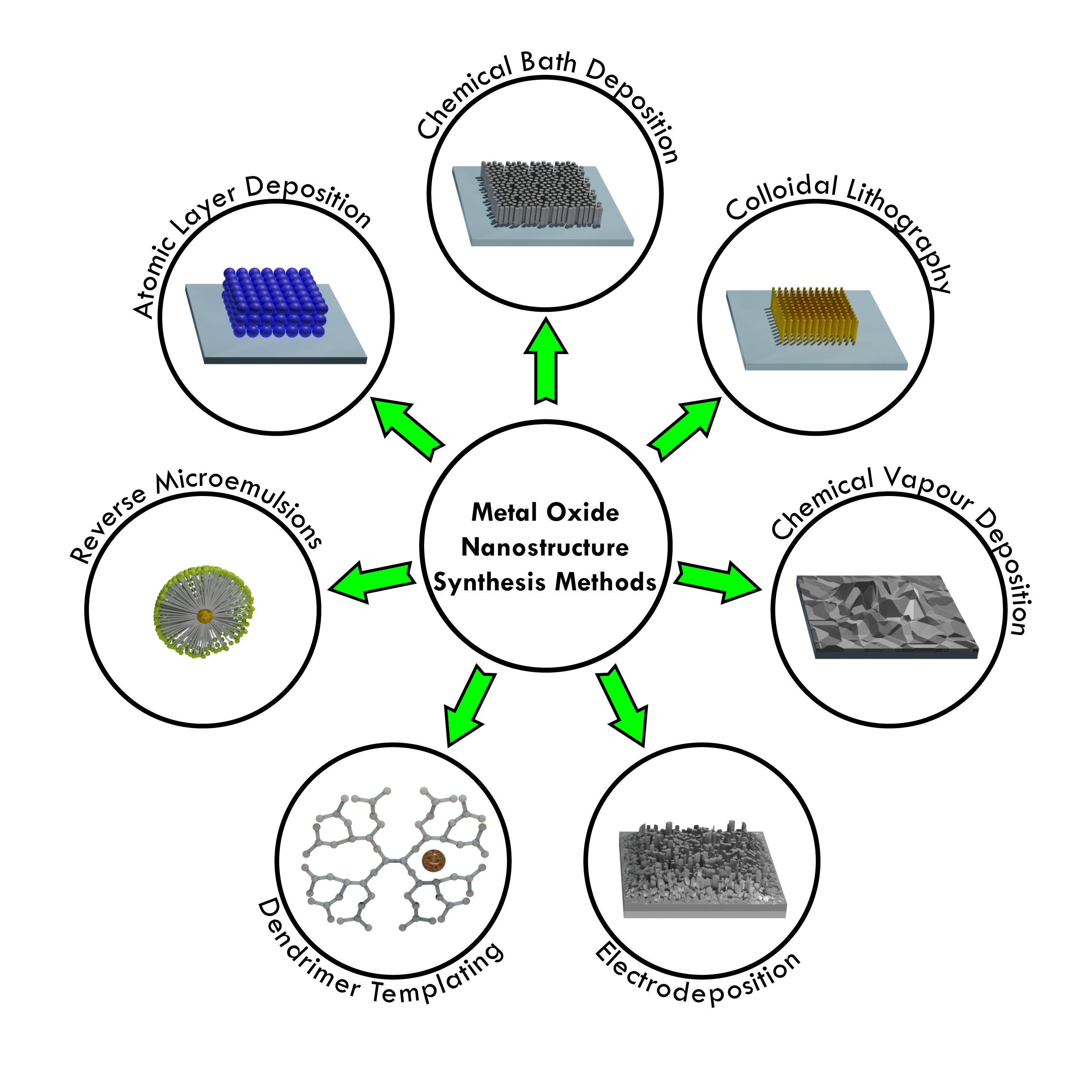
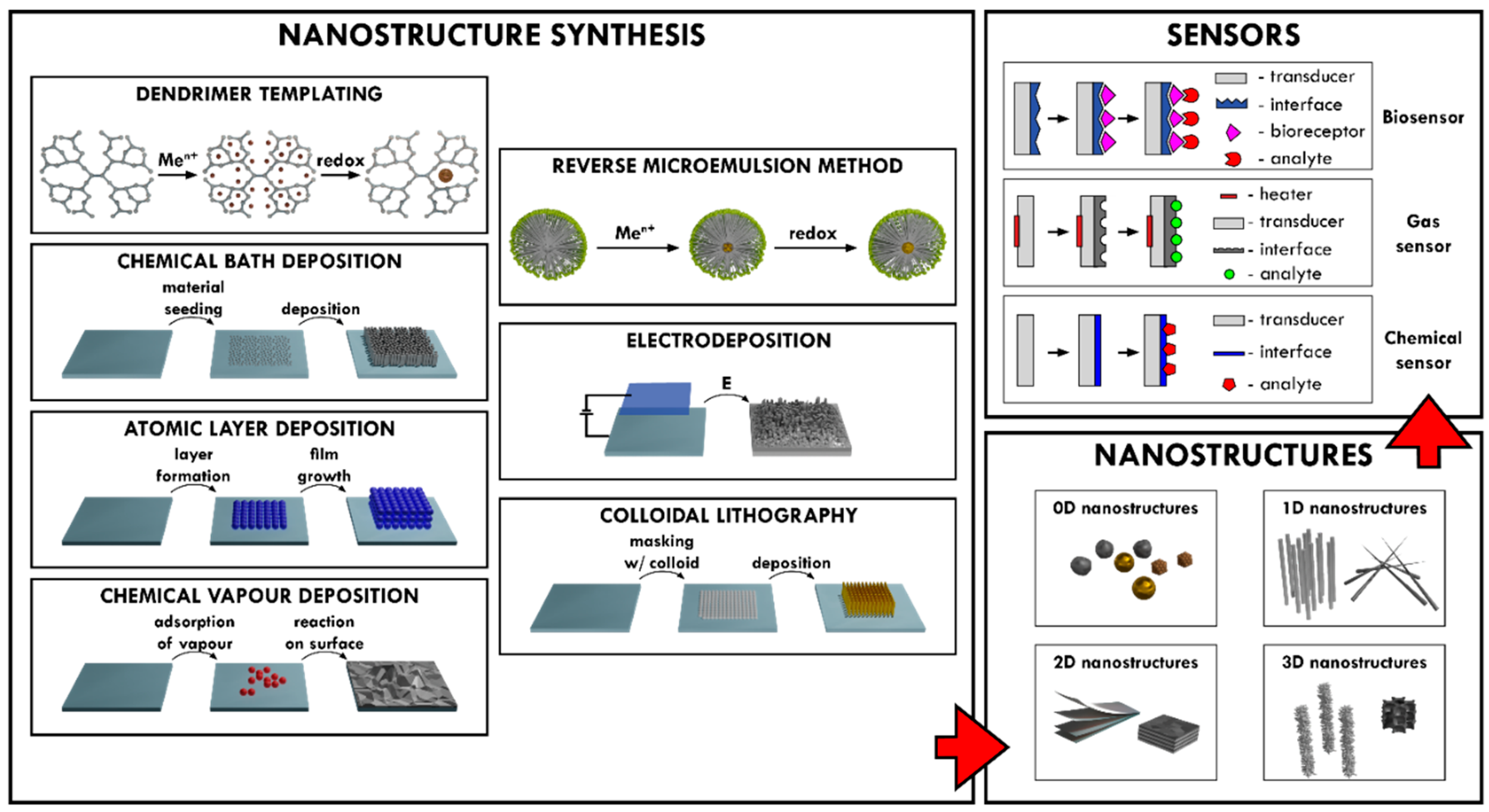
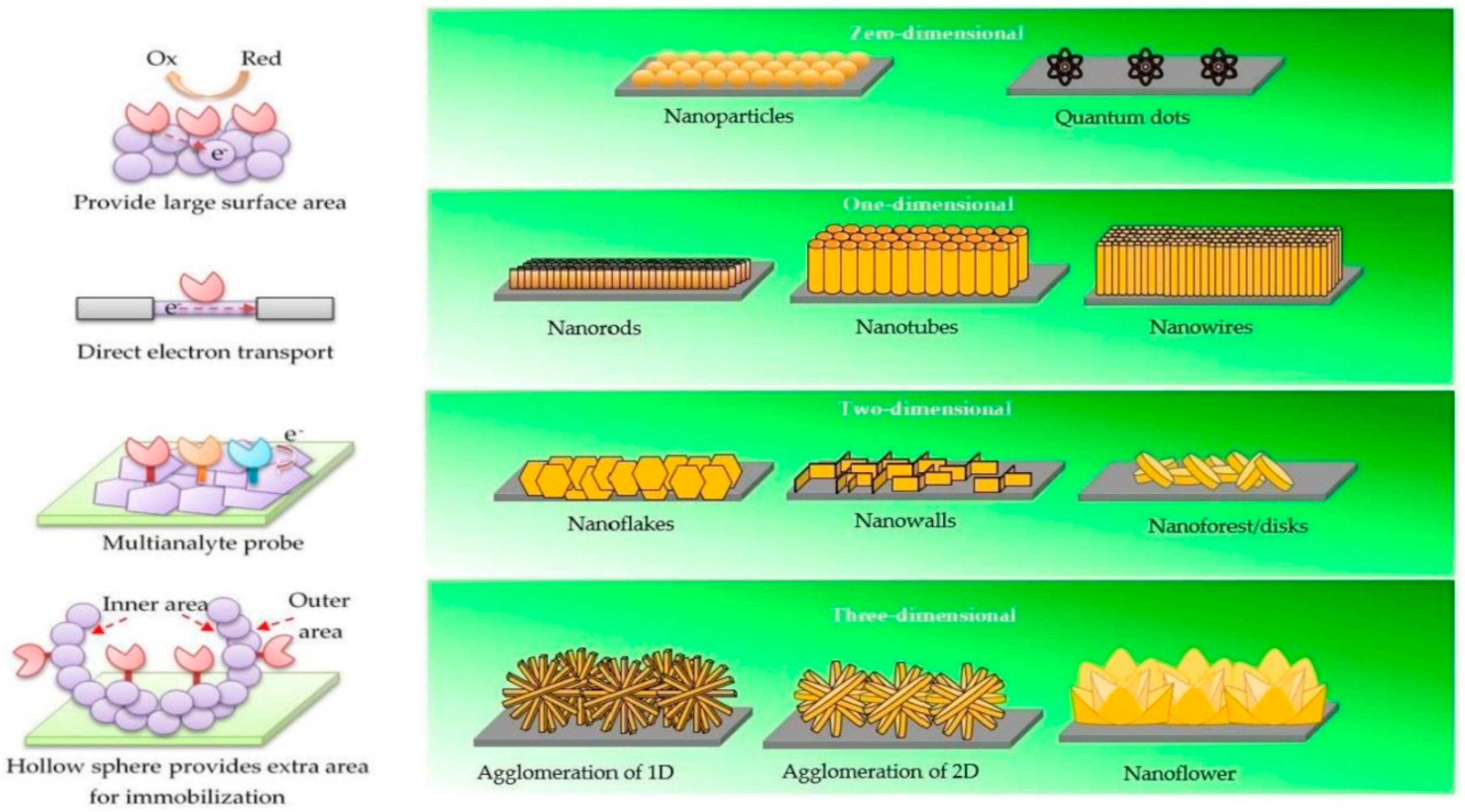
2. Nanostructure Synthesis Methods

In this review, we present selected synthesis methods most commonly used to form metal oxide nanostructures applied for chemical sensing and biosensing. In the last decade, a large number of publications were dedicated to the presented synthesis methods and for the development of desirable properties from 0D to 3D metal oxide nanostructures. Metal oxide nanostructures can be made as a result of a simple precipitation chemical reaction. These syntheses can be referred to as ‘wet chemical’ methods. However, it can be difficult to achieve precise dimensions and novel morphology of nanostructures using wet chemical methods alone. Therefore, the application of templates, external energy (thermal or electrical), and pressure can lead to more control and more variation in the morphology of the formed metal oxide nanostructures. The presented methods are suitable for the fabrication of metal oxide nanostructures of different sizes and morphologies, which can be used for various target analytes in the development of sensors.

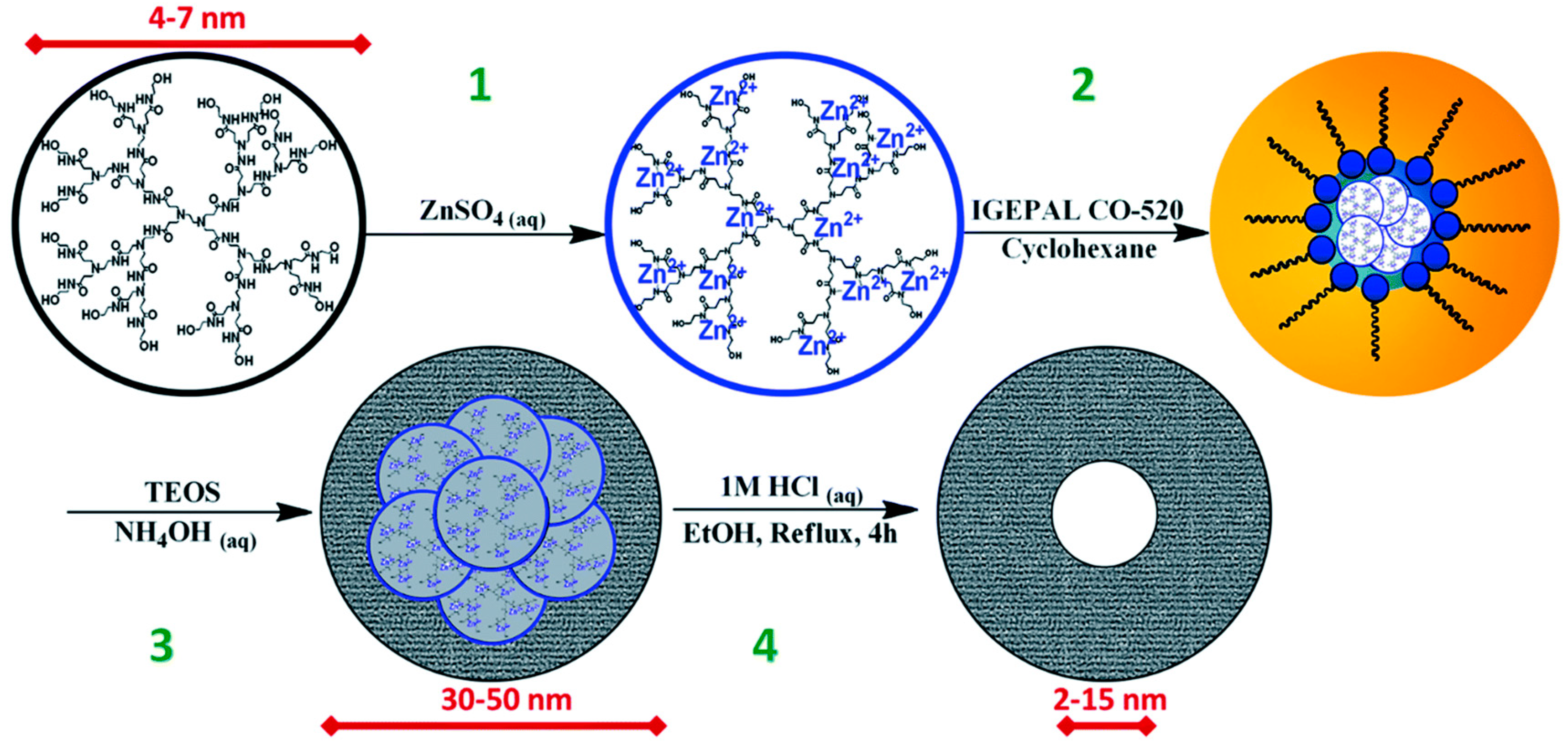
2.1. Reverse Microemulsion Method for the Synthesis of Nanostructures

Synthesis in reverse microemulsions is an avenue for the formation of 0D nanostructures. Microemulsion is an isotropic and thermodynamically stable system of two non-miscible liquids and a surfactant [38]. Depending on the polar/nonpolar fluid ratio, surfactants can be thermodynamically driven to self-assembly generating micelles (in polar surroundings) or reverse micelles (in non-polar surroundings). Usually, 0D nanostructure synthesis is undertaken in reverse micelles, sometimes described as ‘nanoreactors’ [39,40]. This allows the polar and ionic compounds to be separated into isolation from nonpolar surroundings, inside the hydrophilic centers of the reverse micelles. Micelles can, and frequently do, interact with each other, colliding, breaking apart, and exchanging trapped compounds; this is what drives nucleation and growth [41]. The methods for nanostructure synthesis are presented in Figure 1.
In a work by Du et al., 2012, NiO nanoparticles were synthesized in reverse micelles by reducing NiCl2 with aqueous NH3 and calcinated in a furnace. Microemulsion consisted of oil (cyclohexane)/surfactant (Triton X-100)/cosurfactant (n-hexanol)/water (NiCl2 + NH3). By varying the proportions of microemulsion constituent parts, mixing method and calcination temperature, the particle size of NiO was controlled from 11.5 to 31.5 nm. The smallest NiO nanoparticles were synthesized in 44% cyclohexane: 33% Triton X-100: 16% n-hexanol: 7% water solution (inorganic precursors), mixing the microemulsions in a dropwise manner, calcinating in 450 °C for 2 h. Controlling particle size is crucial for sensing application, as lowering the diameter of the NiO particles increased the sensitivity to H2S gas when measured at 150 °C [42]. However, not all syntheses methods require mixing two separate microemulsions to form nanoparticles. Liang et al., 2017, synthesized ultrafine α-Fe2O3 nanoparticles using the microemulsion method. The solution consisted of Fe(NO3)3, NaCl, deionised water, CTAB, benzene, and was stirred at 70 °C for 6 h. The temperature was then increased to 90 °C for azeotrope distillation to remove the water. The dried sample was calcinated for 5 h at 500 °C. The resultant particles have a narrow distribution, spanning from 2.3 to 3.9 nm [43]. Ali et al., 2019, produced well defined V-doped ZnO nanoparticles by microemulsion, with a tunable band gap based on incorporated vanadium amount [44].

2.2. Dendrimer Templating for Nanostructure Formation

Dendrimers are monodisperse macromolecular structures with extending branches from the center, highly symmetrical and exhibit 3D or 0D morphology, which is essential for not only the formation but the stabilization of 0D nanostructures [45,46]. Generally, for metal nanocluster synthesis, metal ions are incorporated inside the dendrimer structure by coordinative interaction with functional groups of dendrimer interior. Then, trapped ions are chemically reduced to form nanoclusters with a defined number of atoms. The number of atoms in a cluster can be controlled by changing the encapsulating dendrimer [47].
Dendrimers are used not only for 0D metal oxide nanostructure synthesis but also as stabilizers. In the study by Nakanishi and Imae, 2005, TiO2 nanoparticles were formed by hydrolysis of TiCl4 in water with and without dendrimers. Liquid TiCl4 (−20 °C) was added to a solution at pH 10 in the presence and absence of G4.5-COONa dendrimer under stirring and maintained 0 °C. TiO2 nanoparticles were evaluated and their diameters compared. The TiO2 nanoparticles synthesized without the use of dendrimers were larger and dependent on the pH of the solution, while the average size of the particles formed inside the dendrimers was smaller (7.5 nm for non-dendrimers and 4.4 to 6.7 nm for dendrimer-protected) and the particle size depended on the dendrimer terminal groups. Additionally, suspensions of dendrimer-protected nanoparticles were stable over several months, as the dendrimer coating prevents TiO2 NPs from aggregating [48]. A comparative study was conducted by Vijayalakshmi et al., 2020, on stabilizing agents of polyvinylpyrrolidone (PVP), glycodendrimer, and chalcone dendrimer for Ag@SnO2 nanoparticle synthesis. Ag core-SnO2 shell nanoparticles were synthesized by the redox-transmetalation method, using stabilizing agents that result in nanoparticles of 30–40 nm diameter with similar structural parameters and indirect band gap energy of 3.84–4.0 eV. Photoluminescence studies identified that Ag@SnO2 nanoparticles emitted photons in UV. The antibacterial and antifungal properties were tested with mixed results [49]. Dendrimer templating can also be used as a part in multi-step synthesis. The following development of microporous SiO2 nanoparticles was published by Rosenberg et al., 2019: microporous SiO2 nanoparticles were synthesized by silanization in the reverse microemulsion of Zn2+- and Cu2+-loaded dendrimers. A scheme for total synthesis is depicted in Figure 2. The composition of the reverse microemulsion system, in addition to varying the dendrimer generation, allowed for the control of microporous SiO2 nanoparticle generation with a particle size of 20–50 nm and a micropore size of 2–15 nm. Dendrimers loaded with Cu2+ produced larger micropores than Zn2+, while empty dendrimers did not provide micropore formation.

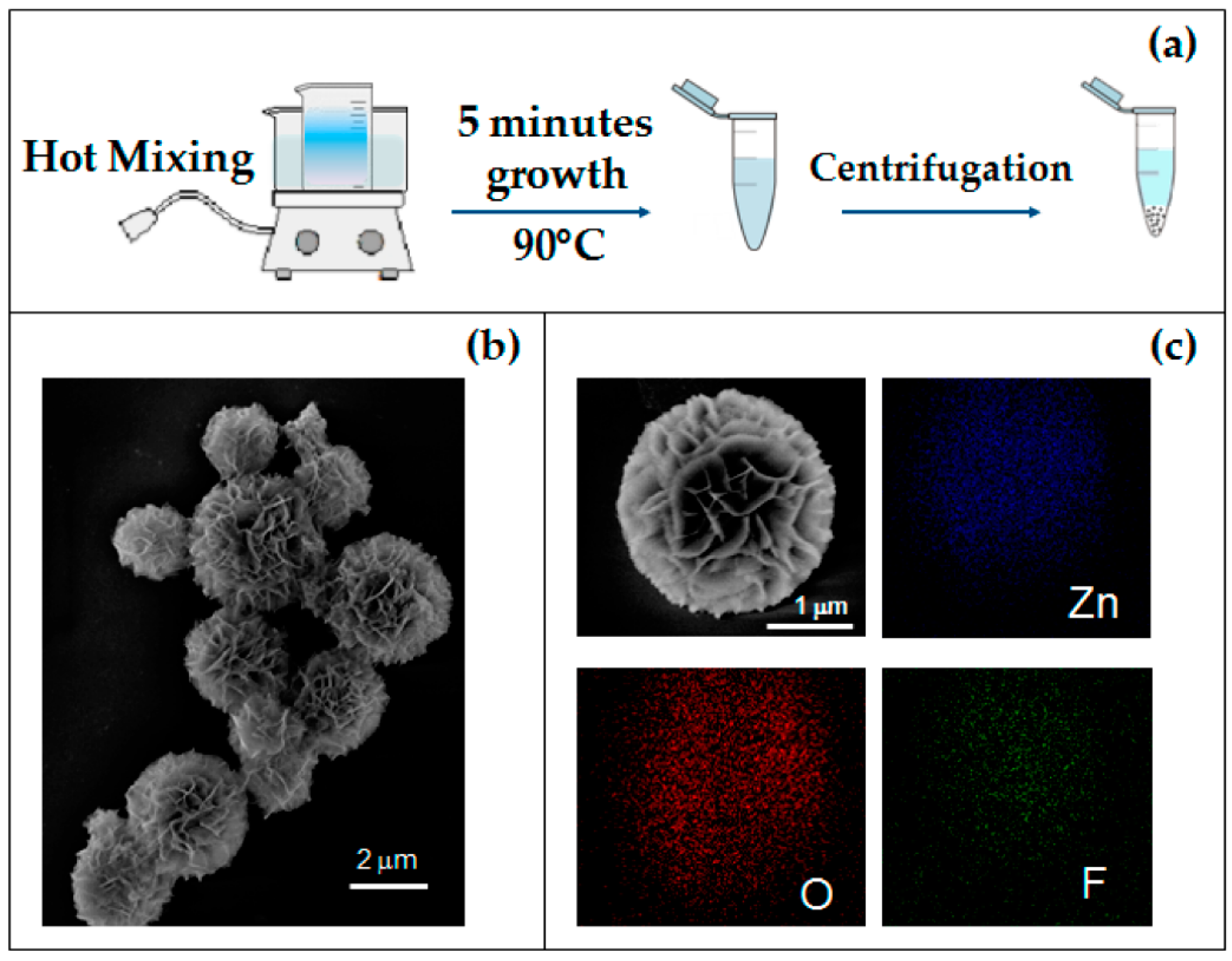
2.3. Chemical Bath Deposition (CBD) for Nanostructure Synthesis

CBD can be considered to be the simplest method for depositing films of semiconductors or metal oxides. The procedure is generally performed from aqueous solutions where the material is generated and deposited on the substrate in the same bath. The method requires minimal substrate preparation and can be used to deposit films on any substrate as long as it is chemically stable while in deposition solution. Glass is a common choice when transparency is necessary [50]. Plastics can also be used as a substrates; however, their adhesive properties to deposited material can vary, meaning surface treatment before deposition may be required [51,52]. Monolayers (for example, silanes) with specific functional groups can be used to coat the substrate and direct the deposition toward (with hydrophilic groups) or away from (with hydrophobic groups) specific areas in an attempt to create patterned surface depositions [53,54,55]. ZnO nanostructures, named microflowers (MFs), have been formed by a chemical bath deposition method by Strano et al. The formed nanostructures are presented in Figure 3 [56].
CBD can be utilized to form films on substrates of any shape. In the work by Chua et al., 2021, MoO3 nanorods were deposited on tapered optical fiber for room temperature ammonia sensors. The deposition was carried out in an aqueous solution mixture of 0.1 M Na2MoO4 and 0.65 M HNO3 solution at 85 °C, in a two-step synthesis. First, the optical fibers were immersed in synthesis solution for 20 min to form MoO3 nucleates, rinsed with deionized water and placed back in synthesis solution for 10 min to grow MoO3 nanorods. Optic fiber with MoO3 deposition was then annealed. Few annealing temperatures were chosen, with 150 °C having the best results for optical ammonia sensor [57]. Nanostructures of ZnO are widely deposited using the chemical bath deposition method. In this work by Vessalli et al., 2017, ZnO nanorods (ZnO NRs) were grown with graphene oxide (GO) to form a composite material. The ZnO NRs were deposited in Zn(NO3)2 HMTA solution: (1) on ZnO seed layer, (2) on GO layer, and (3) with added GO in solution. This resulted in three different sensors to volatile organic compounds (VOCs) of varied selectivity. This change in selectivity is explained by the sensor’s change in resistance when GO is deposited under ZnO NRs. When the sensor was modified with GO deposition under and on ZnO NRs, better sensor selectivity was achieved [58]. Husham et al., 2017, introduced a synthesis of ZnO NRs from Zn(NO3)2 and HMTA solution using microwave-assisted CBD to form a metal-semiconductor-metal-based UV sensor. The ZnO seeding layer was deposited by RF sputtering on clean Si substrate and annealed at 400 °C for 1 h. ZnO NRs were grown in Zn(NO3)2, HMTA solution at 90 °C for 2 h, heated by microwave heating. Aluminum and palladium contacts were deposited to utilize ZnO NRs for UV sensing. Grown ZnO NRs show vertical alignment and low defect density. A device based on ZnO NRs show remarkable potential for low-/self-powered sensor [59]. Gas sensing properties of CBD-formed ZnO nanostructures are also studied widely [60,61,62].

2.4. Electrodeposition for the Formation of Nanostructures

As a deposition method, electrodeposition has many advantages compared to other methods, such as catalyst-free process, a short deposition time, a low deposition temperature and the ability to make homogeneous large-area depositions [63,64]. The flexibility of the electrodeposition method for the formation of ZnO nanostructures was fully shown in a study by Chen et al., 2013. The ZnO nanostructure deposition from the Zn(NO3)2 electrolyte with KCl was analyzed by looking at the effects of Zn(NO3)2, KCl concentrations, deposition temperature and deposition voltage. An increase in KCl supporting electrolyte concentration from 0 to 1 M created ZnO depositions of varied structures from microspheres (0.03 M KCl) to nanosheets (0.1–1 M KCl). Running an electrodeposition with high KCl concentrations also forms zinc hydroxyl compounds alongside ZnO, with the decomposition of the former in high temperatures potentially leading to the formation of porous ZnO nanosheets. An increase in the concentration from 0.005 to 0.5 M creates ZnO depositions from nanospikes (0.005–0.02 M) to nanosheets (0.1–0.5 M). Deposition temperature also has an effect on electrodeposited nanostructures, with deposited structures changing from nanowires to nanosheets with increasing temperature. Increasing the deposition potential seems to increase the density of nanostructures; it also promotes the formation of zinc hydroxyl compounds along with ZnO [65]. Mollarasouli et al., 2020, used the two-step electrodeposition method to form NiWO4 nanostructures for non-enzymatic glucose sensor. The first step was the deposition of Ni-W metal alloy under –1.4 V for 60 s using 0.67 mM NiSO4, 0.3 mM Na3WO4, 0.26 mM citric acid, and 31 mM Na2SO3. The pH was adjusted to 8.0, for the citrate to form complex with Ni and W. The second step involved formation of NiWO4 from deposited Ni-W alloy by cyclic voltammetry in 1 M NaOH for 15 cycles at 50 mV s−1. CV treatment under basic conditions with low scan rate is required for the diffusion of OH anions to the Ni-W alloy [66]. Patella et al., 2022, developed an immunosensor based on ZnO NRs fabricated by electrodeposition. Indium tin oxide on polyethylene terephthalate (ITO-PET) was used as a flexible substrate and ZnO NRs were deposited with optimized conditions of −0.95 V vs. Ag/AgCl, for 60 min in 10 mM ZnCl2 and 10 mM NaNO3 at pH 4.5, resulting in hexagonal ZnO NRs with 800 nm mean length. The schematic representation of ZnO nanorods formed using the electrodeposition method and application in sandwich format immunosensor designed for human immunoglobulin G detection is presented in Figure 4 [67].

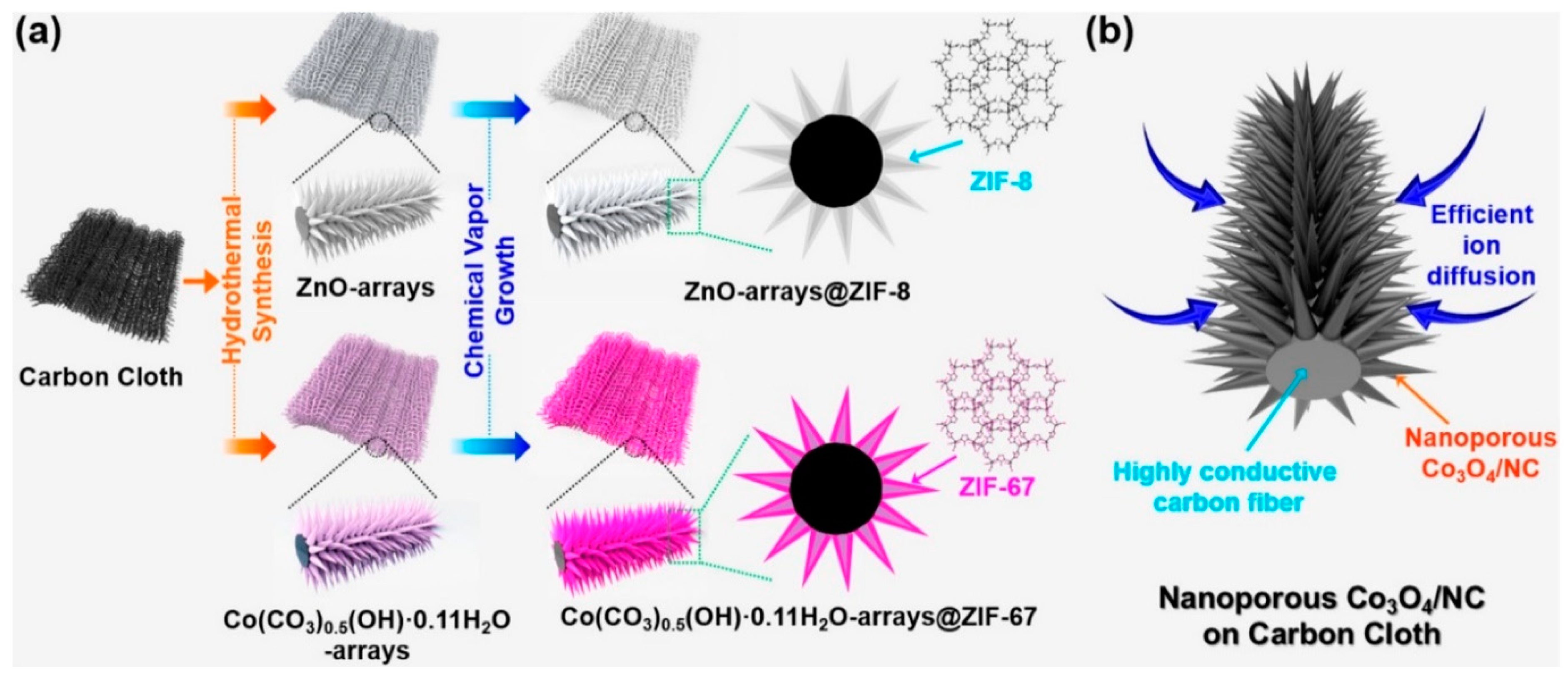
2.5. Chemical Vapor Deposition (CVD) for Synthesis of Nanostructures

It is a well-known and widely applied technique for solid phase material formation [68,69,70,71]. Unlike physical vapor deposition, which requires sputtering or evaporation, CVD is a method in which the precursor material is thermally decomposed or chemically reacts on the substrate and is allowed to grow, producing a thin film. The growth of thin films is regulated by temperature, concentration of reactants, and pressure [72]. There are modified CVD procedures, for example: plasma-enhanced chemical vapor deposition (PECVD), where plasma is created of the reacting gases and deposition occurs, low-pressure chemical vapor deposition (LPCVD) and atmospheric pressure chemical vapor deposition (APCVD) [73,74,75]. Deposition using CVD on substrates with 3D morphology has been tested and offered promising applications. A process for metal-organic-framework growth on carbon cloth was tested. ZnO and cobalt carbonate hydroxide (Co(CO3)0.5(OH)∙0.11H2O) were deposited on carbon cloth. Using CVD, the ZnO layer was converted into ZnO@ZIF-8 using 2-methylimidazole (2-Melm) vapor at 100 °C, while (Co(CO3)0.5(OH)∙0.11H2O) was converted into Co(CO3)0.5(OH)·0.11H2O@ZIF-67. Subsequent heat treatment for the Co(CO3)0.5(OH) < 0.11H2O sample resulted in the formation of CoO3 and nanoporous carbon (CoO3/NC), creating an electrode exhibiting excellent electrochemical performance (Figure 5).
In a work by Barreca et al., 2010, 1D ZnO nanostructures of high aspect ratio were grown on alumina substrates at 300 °C by PECVD for the application of CO, H2 and CH4 gas sensors. CVD precursors were obtained by reaction of diethyl zinc with neutral ketoiminate in hexane. For CO and CH4, best sensing temperature was 200 and 300 °C, respectively. For H2 gases, the sensing ability increased with increasing temperature, with the best response to H2 gases at a maximum measured temperature of 400 °C [76]. Zhang et al., 2012, produced a gas sensor for NO2, CH4 and CO based on 1D SnO2 nanobelts formed from high-purity Sn powder modified with gold (Au). SnO2 nanobelts were formed using the water-assisted CVD method at 850 and 1000 °C. Au modification plays a crucial role in the formation of the SnO2 nanobelts as a structure directing agent [77]. A modification of quartz crystal microbalance (QCM) sensor was published by Wu et al., 2020, Mg-ZnO nanostructures were directly grown by MOCVD at 500 °C using diethyl zinc, bis-methyl-cyclopentadienyl magnesium, and oxygen, resulting in uniform NRs of 405 nm in average height. Formation of 1D nanostructures greatly increased the surface area of the sensor, and Mg inclusion to the nanostructure stabilizes the ZnO denying the release of toxic Zn2+ ions, thus minimizing the toxicity to microorganisms [78]. A gas sensor for ethanol and acetone was formed on fluorine-doped and undoped Co3O4 nanodeposits grown on alumina substrates by Barreca et al., 2011. Two precursors enabled the synthesis using PECVD of fluorine-doped and undoped Co3O4. This resulted in a favorable influence of fluorine on the Co3O4 system. The introduction of fluorine into deposition created a more responsive gas sensor and lowered its working temperature, both features are highly regarded in technological application [79].

2.6. Atomic Layer Deposition (ALD) Method for the Formation of Nanostructures

ALD is a subclass of CVD in which the process is self-limiting and requires the separation of precursor materials and the introduction to the substrate in sequence [80]. Deposition happens in cycles with a given amount of material deposited per cycle, from less than 0.2 to 12 nm per cycle [81]. ALD can be applied to form thin 2D metal oxide nanostructures that usually are amorphous due to low deposition temperatures, and require post deposition treatment or deposition at a higher temperatures [82]. ALD can be applied for deposition on more complex substrates (2D, 3D nanostructures) and on variety of materials: metals, glasses, oxides, graphene, and polymers [83,84,85,86,87,88]. Water-soluble polymers can be coated with ALD and used as sacrificial layers to form free-floating 2D structures [89]. ALD is considered to be the main method of choice for conformal deposition of thin film/monolayer metal oxide, sulphide, and nitride formation on complex nanostructures, despite the wasteful usage of energy and reagents [80,90].
As mentioned above, ALD-based nanostructures and nanolayer depositions can be used on complex nanostructures for the uniform deposition of functional material. Recently, ZnO nanostructure application in biosensor design became a hot topic. ZnO has high isoelectric point and this feature makes it a good candidate for biosensor applications. Moreover, it can be mass produced due to its cost-effectiveness, it is nontoxic, it is chemically stable and different nanostructures can be formed. The different dimensions of the ZnO nanostructures with their advantages are presented in Figure 6 [27].
Chaaya et al., 2014, proposed the deposition of ZnO thin films by ALD on electrospun poly(acrylonitrile) (PAN) fibers, to enhance the UV detection capabilities. Diethyl zinc (DEZ) and H2O were used as precursors for the deposition of ZnO ALD. The effects on the sensitivity of the UV sensor of the deposition cycle number, temperature, and electrospinning increased the photoresponsive current of UV by a factor of 250 compared to a flat electrode. This increase in sensitivity comes from an increase in surface area, with smaller grain sizes having a more positive UV photoresponse [16]. The ALD technique has advantages in comparison to other chemical deposition methods, namely, the deposited material is conformal, pinhole-free, has good adhesion to the substrate and is suitable for periodic nanostructures, such as nanolaminates, and periodic coating of multiple materials of thickness in the nanoscale formations [16,91,92,93,94]. In the article by Balevicius et al., 2018, Al2O3/ZnO nanolaminates were formed by ALD and tested for optical biosensor application using total internal reflection ellipsometry (TIRE). Nanolaminates were formed on glass substrates from DEZ and H2O for ZnO and trimethylaluminium (TMA) and H2O for Al2O3, and deposition was performed at fixed 100 °C. The samples had a total thickness of 200 nm, consisting of (i) four alternating Al2O3 and ZnO layers of 50 nm thickness and (ii) two Al2O3 and ZnO layers of 100 nm thickness. When comparing the two nanolaminate structures, a higher sensitivity was achieved using 50 nm layers of Al2O3 and ZnO. This increased sensitivity was explained by multiple reflections from the layer boundaries [1].
Lou et al., 2021, proposed the use of ALD for the formation and application of formaldehyde detection. Hydrothermally synthesized powdered SnO2 nanospheres were coated with ZnO using ALD at 180 °C using DEZ and H2O, and they were annealed at 400 °C for 2 h. SnO2/ZnO heterojunction formation using ALD created a superior nanosphere gas sensor compared to SnO2 nanospheres, the optimal working temperature was lowered by 40 °C and reached 200 °C, and sensor response was increased by a factor of 7 [95].

3. Application of Metal Oxide Nanostructures for Chemical Sensing and Biosensing

In 1962, Clark and Lyons presented the idea of the biosensor and suggested that enzymes may be immobilized on electrical detectors to create enzyme electrodes. Using glucose oxidase (GOx), the first enzyme electrode was developed to track blood glucose levels [96]. A biosensor is an analytical system consisting of a biological sensing component connected to a transducer that transforms biochemical reactions into an electrical or optical signal that is proportional to the concentration of the targeted analyte.
Biosensor technology has received interest in the last decade and has been applied in many areas: food, environment, and healthcare [97,98]. Biosensors have a very broad definition; they can be classified by bioreceptor type (enzyme, antibody, DNA, cells, biomimetic) and by signal transduction (optical, calorimetric, piezoelectric, electrochemical) [99]. There is plenty of application for nanostructures to be utilized in signal transducing as signal enhancers. The nanostructure formation methods and application in biosensor design are summarized in Table 1.
Faria and Mazon, 2019, fabricated electrochemical immunosensors based on ZnO nanowires (NWs) to diagnose early-stage Zika virus infection from patient urine. ZnO NWs were deposited using the CBD method on a graphene-modified Au printed circuit board. Such modification has potential in lowering the limit of detection (LOD) by increasing the surface area of the electrode, as well as providing a surface with high chemical stability, thus having a suitable surface for antibody immobilization. Monoclonal Zika virus antibodies (ZIKV-NS1) were immobilized on the ZnO NW using cystamine (Cys) and glutaraldehyde (GA), and a diluted solution of antibodies was dropped on the surface and left to incubate for 12 h. Calibration of the sensor was performed, achieving good linearity in the 0.1–100 ng/mL range of ZIKV-NS1 and a low LOD of 1 pg/mL, showing potential in application as a rapid point-of-care test [100].
In the work by Buzavaite-Verteliene et al., 2020, the TIRE method was used for the study of the excitation and sensitivity properties of the hybrid Tamm plasmon polariton-surface plasmon polariton (TPP-SPP) and single surface plasmon resonance (SPR) modes of immobilization of bovine serum albumin (BSA) and the granulocyte colony stimulating factor receptor (GCSF-R) on the surface. The plasmonic photonic nanostructure was formed from high (TiO2) and low (SiO2) refractive index bilayers covered by a thin (40 nm) Au layer. The SPP component (δΔh-SPP/δλ = 53.9°/nm) of the hybrid TPP-SPP mode showed 6.4 times higher sensitivity than the single SPR (δΔSPR/δλ = 8.4°/nm) during the formation of the bovine serum albumin (BSA) layer on the Au film. The sensitivity using the hybrid plasmonic mode was found to be controlled by using the strong coupling effect between the components of TPP and SPP. Two optical sensor geometries are presented in Figure 7 [105].
In the work by Plikusiene et al., 2021, the formation of 1D plasmonic photonic structures from TiO2 and SiO2 nanolayers on the commercially available quartz crystal microbalance with dissipation (QCM-D) sensors chip was reported. This thin Au film is able to generate Tamm plasmon polaritons and cavity modes that can enhance the optical signal of spectroscopic ellipsometry (SE) without using a coupler, as is usually necessary for the excitation of surface waves applied for biosensing [109,110,111,112]. The scanning electron microscope (SEM) micrograph of the nanostructures used for Tamm plasmons and cavity mode (CM) excitation, formed on the QCM-D sensor disc, is presented in Figure 8.
The Tamm plasmon optical state and CM for the modified QCM-D sensor disc showed sensitivity of ellipsometric parameters to refractive index unit (RIU) as follows: ΨTPP = 126.78 RIU−1 and ΔTPP = 325 RIU−1, and ΨCM = 264 RIU−1 and ΔCM = 645 RIU−1, respectively. This study shows that Tamm plasmon and CM have 23 and 49 times better performance of ellipsometric parameters, respectively, for refractive index sensing than standard SE signal on a QCM-D sensor chip [106].
A chemical sensor is a system that produces a useful signal as a result of a chemical interaction, both qualitative and quantitative. This system contains a transducer domain and a chemical interface layer. At a chemical interface, an analyte chemically reacts with a surface and creates a change in chemical or physical properties; this change is then measured by the transducer and generates an electrical signal proportional to the analyte concentration. Chemical sensors are classified by their transduction method (optical (refractometric, ellipsometric), electrical (conductometry, amperometry), and mechanical (QCM-D)) as well as their structure/composition of the chemical interface layer (metal, metal oxide, and metal semiconductor) [113]. The summary on nanostructures used for chemical sensing is presented in Table 2.
Rahman et al., 2020, published work on modifying a glassy carbon electrode (GCE) with nickel-doped ZnO (Ni-ZnO) nanostructures in Nafion solution to form an electrochemical hydrazine sensor. A three-electrode system was used for electrochemical analysis, and Ag/AgCl, Ni-ZnO/Nafion/GCE, and Pt were used as reference, working, and counter electrodes, respectively. The Ni-ZnO/Nafion/GCE sensor for hydrazine detection was employed in the phosphate buffer system in room-temperature conditions. The sensor exhibited excellent sensitivity with a linear response from 0.2 nM to 0.02 M with an LOD of 1.7 pM. This sensitivity can be explained by the hydrazine detection mechanism. When the Ni-ZnO surface is exposed to hydrazine, surface-mediated hydrazine oxidation takes place, producing N2H4 decomposition and delivery of electrons onto Ni-ZnO; at the same time, OH removal lowers the conduction band of Ni-ZnO, yielding a shift of the current during electrochemical investigation. This shift effect, along with an injection from hydrazine oxidation, produces an increased number of electrons, enhancing the conductance of the electrode. A real sample analysis of industrial effluent water and wastewater showed ~100% recovery of hydrazine from sample solutions, thus concluding its suitability to determine hydrazine in real aqueous samples [122].
In a study by Shetti et al., 2019, an electrochemical sensor was manufactured using Ag-doped TiO2 nanoparticles (Ag-TiO2 NPs) mixed with multi-walled carbon nanotubes (MWCNTs) for the detection of cetirizine, an anti-inflammatory drug. The electrochemical sensor is based on the modified carbon paste electrode, by blending MWCNTs and Ag-TiO2 NPs together with graphite powder and homogenizing with paraffin oil. This results in a sensor that exhibits a higher peak current with a less positive potential for cetirizine oxidation than for an unmodified electrode; however, the oxidation of cetirizine was found to be irreversible. Both Ag-TiO2 and MWCNT have a positive effect on enrichment in cetirizine oxidation, playing significant roles in the fast electron transfer process. This enables the sensor to detect cetirizine in very low amounts with LDR from 0.3 to 3 μM and an LOD of 8.76 nM [118].

4. Conclusions

Recently, progress and advances in the synthesis methods and application area of various metal oxide nanostructures illustrate the great relevance and necessity of such structures in the design of different types of sensors. The present review summarizes progress and advances in the synthesis methods of various 0D, 1D, 2D, and 3D metal oxide nanostructures and their application in chemical sensors and biosensors for different target analytes’ detection.
The 0D nanostructures, formed by microemulsion or co-precipitation/reduction methods, can be successfully applied in highly sensitive chemical sensors and biosensor design. Efficient synthesis of 0D nanostructures lies in the control of the nanoparticle formation process. However, these methods usually require expensive, complex or wasteful protocols; thus, more simple methods with less size control tend to be preferred. Simple, time-saving and convenient methods of synthesis, such as chemical bath deposition, can be used to form 1D metal oxide nanostructures. Biosensors in which such structures were applied exhibit enhanced sensitivity due to the high surface area, especially in hollow 1D nanostructures. The development of optical biosensors requires one to form nanostructures that can tune and enhance optical signal for the detection of target biological substances. In this case, 2D nanostructures or thin films that can be formed by the ALD method are frequently applied. Novel structures, a high surface-to-volume ratio, and the porosity of 3D nanostructures formed by the wet chemical method allowed to achieve an extremely low LOD and opened a new way of forming 3D nanostructures in electrochemistry-based chemical sensors and biosensors. Flower-like MoO3/In2O3 microstructures formed by the hydrothermal method and composed of numerous nanosheets are promising for the development of gas sensors [123].
However, there is still room for improvement and challenges related to different synthesis methods. Improvements and more research are required to form nanostructures without side effects and with the desired properties for the development of sensitive, reproducible, easy to use, and fast biosensors with minimal pollution of the living nature. The achievement of high stability and nontoxicity in various nanostructures formed from metal oxides, such as ZnO, TiO2 or SiO2, which are applied in vivo biosensing and are exposed by different liquid ambient, is still an issue. Therefore, we expect significant experimental and theoretical research activity regarding the synthesis methods for metal oxide nanostructures of different properties and application for sensing.

Author Contributions

Conceptualization, V.M. and I.P.; methodology, V.M., I.P., and A.R.; writing—original draft preparation, V.M., I.P. and A.R.; writing—review and editing, V.M., I.P. and A.R.; visualization, V.M.; supervision, I.P. and A.R.; project administration, A.R.; funding acquisition, A.R. All authors have read and agreed to the published version of the manuscript.

Funding

This work is part of a project that has received funding from the European Union’s Horizon 2020 research and innovation program under grant agreement No 778157 CanBioSe.

Institutional Review Board Statement

Not applicable.

Informed Consent Statement

Not applicable.

Data Availability Statement

Not applicable.

Conflicts of Interest

The authors declare no conflict of interest.

References

  1. Balevicius, Z.; Paulauskas, A.; Plikusiene, I.; Mikoliunaite, L.; Bechelany, M.; Popov, A.; Ramanavicius, A.; Ramanaviciene, A. Towards the application of Al2O3/ZnO nanolaminates in immunosensors: Total internal reflection spectroscopic ellipsometry based evaluation of BSA immobilization. J. Mater. Chem. C 2018, 6, 8778–8783. [Google Scholar] [CrossRef]
  2. Maciulis, V.; Malinovskis, U.; Erts, D.; Ramanavicius, A.; Ramanaviciene, A.; Balevicius, S.; Juciute, S.; Plikusiene, I. Porous aluminium oxide coating for the development of spectroscopic ellipsometry based biosensor: Evaluation of human serum albumin adsorption. Coatings 2020, 10, 1018. [Google Scholar] [CrossRef]
  3. Plikusiene, I.; Maciulis, V.; Graniel, O.; Bechelany, M.; Balevicius, S.; Vertelis, V.; Balevicius, Z.; Popov, A.; Ramanavicius, A.; Ramanaviciene, A. Total internal reflection ellipsometry for kinetics-based assessment of bovine serum albumin immobilization on ZnO nanowires. J. Mater. Chem. C 2021, 9, 1345–1352. [Google Scholar] [CrossRef]
  4. Filipovic, L.; Selberherr, S. Application of Two-Dimensional Materials towards CMOS-Integrated Gas Sensors. Nanomaterials 2022, 12, 3651. [Google Scholar] [CrossRef] [PubMed]
  5. Tyagi, D.; Wang, H.; Huang, W.; Hu, L.; Tang, Y.; Guo, Z.; Ouyang, Z.; Zhang, H. Recent advances in two-dimensional-material-based sensing technology toward health and environmental monitoring applications. Nanoscale 2020, 12, 3535–3559. [Google Scholar] [CrossRef]
  6. Ponzoni, A.; Baratto, C.; Cattabiani, N.; Falasconi, M.; Galstyan, V.; Nunez-Carmona, E.; Rigoni, F.; Sberveglieri, V.; Zambotti, G.; Zappa, D. Metal oxide gas sensors, a survey of selectivity issues addressed at the SENSOR lab, Brescia (Italy). Sensors 2017, 17, 714. [Google Scholar] [CrossRef] [Green Version]
  7. Zhao, Z.; Zhang, J.; Wang, W.; Sun, Y.; Li, P.; Hu, J.; Chen, L.; Gong, W. Synthesis and electrochemical properties of Co3O4-rGO/CNTs composites towards highly sensitive nitrite detection. Appl. Surf. Sci. 2019, 485, 274–282. [Google Scholar] [CrossRef]
  8. Popov, A.; Lisyte, V.; Kausaite-Minkstimiene, A.; Bernotiene, E.; Ramanaviciene, A. Experimental Evaluation of Quantum Dots and Antibodies Conjugation by Surface Plasmon Resonance Spectroscopy. Int. J. Mol. Sci. 2022, 23, 12626. [Google Scholar] [CrossRef]
  9. Oberdörster, G.; Oberdörster, E.; Oberdörster, J. Nanotoxicology: An emerging discipline evolving from studies of ultrafine particles. Environ. Health Perspect. 2005, 113, 823–839. [Google Scholar] [CrossRef]
  10. Pokropivny, V.V.; Skorokhod, V.V. Classification of nanostructures by dimensionality and concept of surface forms engineering in nanomaterial science. Mater. Sci. Eng. C 2007, 27, 990–993. [Google Scholar] [CrossRef]
  11. Cook, A.W.; Hayton, T.W. Case Studies in Nanocluster Synthesis and Characterization: Challenges and Opportunities. Acc. Chem. Res. 2018, 51, 2456–2464. [Google Scholar] [CrossRef]
  12. Li, Z.; Wang, W.; Yin, Y. Colloidal Assembly and Active Tuning of Coupled Plasmonic Nanospheres. Trends Chem. 2020, 2, 593–608. [Google Scholar] [CrossRef]
  13. García de Arquer, F.P.; Talapin, D.V.; Klimov, V.I.; Arakawa, Y.; Bayer, M.; Sargent, E.H. Semiconductor quantum dots: Technological progress and future challenges. Science 2021, 373, eaaz8541. [Google Scholar] [CrossRef]
  14. Pacholski, C.; Kornowski, A.; Weller, H. Self-assembly of ZnO: From nanodots to nanorods. Angew. Chem.—Int. Ed. 2002, 41, 1188–1191. [Google Scholar] [CrossRef]
  15. Xu, S.; Lei, Y. Template-Assisted Fabrication of Nanostructured Arrays for Sensing Applications. Chempluschem 2018, 83, 741–755. [Google Scholar] [CrossRef]
  16. Chaaya, A.A.; Bechelany, M.; Balme, S.; Miele, P. ZnO 1D nanostructures designed by combining atomic layer deposition and electrospinning for UV sensor applications. J. Mater. Chem. A 2014, 2, 20650–20658. [Google Scholar] [CrossRef]
  17. Wu, C.C.; Pan, T.M.; Wu, C.S.; Yen, L.C.; Chuang, C.K.; Pang, S.T.; Yang, Y.S.; Ko, F.H. Label-free detection of prostate specific antigen using a silicon nanobelt field-effect transistor. Int. J. Electrochem. Sci. 2012, 7, 4432–4442. [Google Scholar]
  18. Ackermann, J.; Metternich, J.T.; Herbertz, S.; Kruss, S. Biosensing with Fluorescent Carbon Nanotubes. Angew. Chem.—Int. Ed. 2022, 61, e202112372. [Google Scholar] [CrossRef]
  19. Aykaç, A.; Gergeroglu, H.; Beşli, B.; Akkaş, E.Ö.; Yavaş, A.; Güler, S.; Güneş, F.; Erol, M. An Overview on Recent Progress of Metal Oxide/Graphene/CNTs-Based Nanobiosensors. Nanoscale Res. Lett. 2021, 16, 65. [Google Scholar] [CrossRef]
  20. Huo, D.; Kim, M.J.; Lyu, Z.; Shi, Y.; Wiley, B.J.; Xia, Y. One-Dimensional Metal Nanostructures: From Colloidal Syntheses to Applications. Chem. Rev. 2019, 119, 8972–9073. [Google Scholar] [CrossRef]
  21. Javed, M.S.; Khan, A.J.; Asim, S.; Shah, S.S.A.; Najam, T.; Siyal, S.H.; Tahir, M.F.; Zhao, Z.; Mai, W. Insights to pseudocapacitive charge storage of binary metal-oxide nanobelts decorated activated carbon cloth for highly-flexible hybrid-supercapacitors. J. Energy Storage 2020, 31, 101602. [Google Scholar] [CrossRef]
  22. Kwak, D.; Wang, M.; Koski, K.J.; Zhang, L.; Sokol, H.; Maric, R.; Lei, Y. Molybdenum Trioxide (α-MoO3) Nanoribbons for Ultrasensitive Ammonia (NH3) Gas Detection: Integrated Experimental and Density Functional Theory Simulation Studies. ACS Appl. Mater. Interfaces 2019, 11, 10697–10706. [Google Scholar] [CrossRef] [PubMed]
  23. Samykano, M. Progress in one-dimensional nanostructures. Mater. Charact. 2021, 179, 111373. [Google Scholar] [CrossRef]
  24. Heard, C.J.; Čejka, J.; Opanasenko, M.; Nachtigall, P.; Centi, G.; Perathoner, S. 2D Oxide Nanomaterials to Address the Energy Transition and Catalysis. Adv. Mater. 2019, 31, e1801712. [Google Scholar] [CrossRef] [PubMed]
  25. Wang, L.; Huang, L.; Tan, W.C.; Feng, X.; Chen, L.; Huang, X.; Ang, K.W. 2D Photovoltaic Devices: Progress and Prospects. Small Methods 2018, 2, 1700294. [Google Scholar] [CrossRef]
  26. Kumar, S.; Pavelyev, V.; Mishra, P.; Tripathi, N.; Sharma, P.; Calle, F. A review on 2D transition metal di-chalcogenides and metal oxide nanostructures based NO2 gas sensors. Mater. Sci. Semicond. Process. 2020, 107, 104865. [Google Scholar] [CrossRef]
  27. Napi, M.L.M.; Sultan, S.M.; Ismail, R.; How, K.W.; Ahmad, M.K. Electrochemical-Based Biosensors on Different Zinc Oxide Nanostructures: A Review. Materials 2019, 12, 2985. [Google Scholar] [CrossRef] [Green Version]
  28. Li, Z.; Zhang, X.; Cheng, H.; Liu, J.; Shao, M.; Wei, M.; Evans, D.G.; Zhang, H.; Duan, X. Confined Synthesis of 2D Nanostructured Materials toward Electrocatalysis. Adv. Energy Mater. 2020, 10, 1900486. [Google Scholar] [CrossRef]
  29. Jang, J.M.; Kim, S.D.; Choi, H.M.; Kim, J.Y.; Jung, W.G. Morphology change of self-assembled ZnO 3D nanostructures with different pH in the simple hydrothermal process. Mater. Chem. Phys. 2009, 113, 389–394. [Google Scholar] [CrossRef]
  30. Chiu, H.Y.; Wi-Afedzi, T.; Liu, Y.T.; Ghanbari, F.; Lin, K.Y.A. Cobalt Oxides with Various 3D Nanostructured Morphologies for Catalytic Reduction of 4-Nitrophenol: A Comparative Study. J. Water Process Eng. 2020, 37, 101379. [Google Scholar] [CrossRef]
  31. Yang, Z.; Lin, Y.; Jiao, F.; Li, J.; Wang, W.; Gong, Y.; Jing, X. Morphology engineering of 3D nanostructure MMNS as bifunctional electrocatalysts towards high-efficient overall water splitting. Appl. Surf. Sci. 2020, 502, 144147. [Google Scholar] [CrossRef]
  32. Tiwari, J.N.; Tiwari, R.N.; Kim, K.S. Zero-dimensional, one-dimensional, two-dimensional and three-dimensional nanostructured materials for advanced electrochemical energy devices. Prog. Mater. Sci. 2012, 57, 724–803. [Google Scholar] [CrossRef]
  33. Joshi, R.K.; Schneider, J.J. Assembly of one dimensional inorganic nanostructures into functional 2D and 3D architectures. Synthesis, arrangement and functionality. Chem. Soc. Rev. 2012, 41, 5285–5312. [Google Scholar] [CrossRef]
  34. Young, C.; Wang, J.; Kim, J.; Sugahara, Y.; Henzie, J.; Yamauchi, Y. Controlled Chemical Vapor Deposition for Synthesis of Nanowire Arrays of Metal-Organic Frameworks and Their Thermal Conversion to Carbon/Metal Oxide Hybrid Materials. Chem. Mater. 2018, 30, 3379–3386. [Google Scholar] [CrossRef]
  35. Altintas Yildirim, O. Efficient vapor-liquid-solid synthesis of copper doped zinc oxide (Cu:ZnO) nanonails with highly homogeneous dopant distribution. Mater. Sci. Semicond. Process. 2019, 101, 238–246. [Google Scholar] [CrossRef]
  36. Pei, Y.; Hu, M.; Xia, Y.; Huang, W.; Li, Z.; Chen, S. Electrochemical preparation of Pt nanoparticles modified nanoporous gold electrode with highly rough surface for efficient determination of hydrazine. Sens. Actuators B Chem. 2020, 304, 127416. [Google Scholar] [CrossRef]
  37. Dondapati, J.S.; Govindhan, M.; Chen, A. Direct growth of three-dimensional nanoflower-like structures from flat metal surfaces. Chem. Commun. 2022, 1, 11127–11130. [Google Scholar] [CrossRef]
  38. Slomkowski, S.; Alemán, J.V.; Gilbert, R.G.; Hess, M.; Horie, K.; Jones, R.G.; Kubisa, P.; Meisel, I.; Mormann, W.; Penczek, S.; et al. Terminology of polymers and polymerization processes in dispersed systems (IUPAC recommendations 2011). Pure Appl. Chem. 2011, 83, 2229–2259. [Google Scholar] [CrossRef] [Green Version]
  39. Ye, Z.; Tan, M.; Wang, G.; Yuan, J. Preparation, characterization and application of fluorescent terbium complex-doped zirconia nanoparticles. J. Fluoresc. 2005, 15, 499–505. [Google Scholar] [CrossRef]
  40. Shlapa, Y.; Sarnatskaya, V.; Timashkov, I.; Yushko, L.; Antal, I.; Gerashchenko, B.; Nychyporenko, I.; Belous, A.; Nikolaev, V.; Timko, M. Synthesis of CeO2 nanoparticles by precipitation in reversal microemulsions and their physical–chemical and biological properties. Appl. Phys. A Mater. Sci. Process. 2019, 125, 1–10. [Google Scholar] [CrossRef]
  41. Malik, M.A.; Wani, M.Y.; Hashim, M.A. Microemulsion method: A novel route to synthesize organic and inorganic nanomaterials. 1st Nano Update. Arab. J. Chem. 2012, 5, 397–417. [Google Scholar] [CrossRef]
  42. Du, Y.; Wang, W.; Li, X.; Zhao, J.; Ma, J.; Liu, Y.; Lu, G. Preparation of NiO nanoparticles in microemulsion and its gas sensing performance. Mater. Lett. 2012, 68, 168–170. [Google Scholar] [CrossRef]
  43. Liang, S.; Li, J.; Wang, F.; Qin, J.; Lai, X.; Jiang, X. Highly sensitive acetone gas sensor based on ultrafine α-Fe2O3 nanoparticles. Sens. Actuators B Chem. 2017, 238, 923–927. [Google Scholar] [CrossRef]
  44. Ali, H.S.; Alghamdi, A.S.; Murtaza, G.; Arif, H.S.; Naeem, W.; Farid, G.; Sharif, S.; Ashiq, M.G.B.; Shabbir, S.A. Facile microemulsion synthesis of vanadium-doped ZnO nanoparticles to analyze the compositional, optical, and electronic properties. Materials 2019, 12, 821. [Google Scholar] [CrossRef] [PubMed] [Green Version]
  45. Rosenberg, D.J.; Alayoglu, S.; Kostecki, R.; Ahmed, M. Synthesis of microporous silica nanoparticles to study water phase transitions by vibrational spectroscopy. Nanoscale Adv. 2019, 1, 4878–4887. [Google Scholar] [CrossRef] [Green Version]
  46. Li, B.; You, N.; Liang, Y.; Zhang, Q.; Zhang, W.; Chen, M.; Pang, X. Organic Templates for Inorganic Nanocrystal Growth. Energy Environ. Mater. 2019, 2, 38–54. [Google Scholar] [CrossRef] [Green Version]
  47. Yamamoto, K.; Imaoka, T.; Tanabe, M.; Kambe, T. New Horizon of Nanoparticle and Cluster Catalysis with Dendrimers. Chem. Rev. 2020, 120, 1397–1437. [Google Scholar] [CrossRef]
  48. Nakanishi, Y.; Imae, T. Synthesis of dendrimer-protected TiO2 nanoparticles and photodegradation of organic molecules in an aqueous nanoparticle suspension. J. Colloid Interface Sci. 2005, 285, 158–162. [Google Scholar] [CrossRef]
  49. Vijayalakshmi, R.V.; Kuppan, R.; Kumar, P.P. Investigation on the impact of different stabilizing agents on structural, optical properties of Ag@SnO2 core-shell nanoparticles and its biological applications. J. Mol. Liq. 2020, 307, 112951. [Google Scholar] [CrossRef]
  50. Hodes, G. Semiconductor and ceramic nanoparticle films deposited by chemical bath deposition. Phys. Chem. Chem. Phys. 2007, 9, 2181–2196. [Google Scholar] [CrossRef]
  51. Thamaraiselvan, C.; Carmiel, Y.; Eliad, G.; Sukenik, C.N.; Semiat, R.; Dosoretz, C.G. Modification of a polypropylene feed spacer with metal oxide-thin film by chemical bath deposition for biofouling control in membrane filtration. J. Memb. Sci. 2019, 573, 511–519. [Google Scholar] [CrossRef]
  52. Breen, M.L.; Woodward IV, J.T.; Schwartz, D.K.; Apblett, A.W. Direct Evidence for an Ion-by-Ion Deposition Mechanism in Solution Growth of CdS Thin Films. Chem. Mater. 1998, 10, 710–717. [Google Scholar] [CrossRef]
  53. Lu, Y.; Meng, X.; Yi, G.; Jia, J. In situ growth of CuS thin films on functionalized self-assembled monolayers using chemical bath deposition. J. Colloid Interface Sci. 2011, 356, 726–733. [Google Scholar] [CrossRef]
  54. Collins, R.J.; Shin, H.; DeGuire, M.R.; Heuer, A.H.; Sukenik, C.N. Low temperature deposition of patterned TiO2 thin films using photopatterned self-assembled monolayers. Appl. Phys. Lett. 1996, 69, 860–862. [Google Scholar] [CrossRef]
  55. Masuda, Y.; Saito, N.; Hoffmann, R.; De Guire, M.R.; Koumoto, K. Nano/micro-patterning of anatase TiO2 thin film from an aqueous solution by site-selective elimination method. Sci. Technol. Adv. Mater. 2003, 4, 461–467. [Google Scholar] [CrossRef]
  56. Strano, V.; Greco, M.G.; Ciliberto, E.; Mirabella, S. Zno microflowers grown by chemical bath deposition: A low-cost approach for massive production of functional nanostructures. Chemosensors 2019, 7, 62. [Google Scholar] [CrossRef] [Green Version]
  57. Chua, W.H.; Yaacob, M.H.; Tan, C.Y.; Ong, B.H. Chemical bath deposition of h-MoO3 on optical fibre as room-temperature ammonia gas sensor. Ceram. Int. 2021, 47, 32828–32836. [Google Scholar] [CrossRef]
  58. Vessalli, B.A.; Zito, C.A.; Perfecto, T.M.; Volanti, D.P.; Mazon, T. ZnO nanorods/graphene oxide sheets prepared by chemical bath deposition for volatile organic compounds detection. J. Alloys Compd. 2017, 696, 996–1003. [Google Scholar] [CrossRef] [Green Version]
  59. Husham, M.; Hamidon, M.N.; Paiman, S.; Abuelsamen, A.A.; Farhat, O.F.; Al-Dulaimi, A.A. Synthesis of ZnO nanorods by microwave-assisted chemical-bath deposition for highly sensitive self-powered UV detection application. Sens. Actuators A Phys. 2017, 263, 166–173. [Google Scholar] [CrossRef]
  60. Wu, T.; Wang, Z.; Tian, M.; Miao, J.; Zhang, H.; Sun, J. UV excitation NO2 gas sensor sensitized by ZnO quantum dots at room temperature. Sens. Actuators B Chem. 2018, 259, 526–531. [Google Scholar] [CrossRef]
  61. Wang, H.; Dai, M.; Li, Y.; Bai, J.; Liu, Y.; Li, Y.; Wang, C.; Liu, F.; Lu, G. The influence of different ZnO nanostructures on NO2 sensing performance. Sens. Actuators B Chem. 2021, 329, 129145. [Google Scholar] [CrossRef]
  62. Yuliarto, B.; Ramadhani, M.F.; Septiani, N.L.W.; Hamam, K.A. Enhancement of SO2 gas sensing performance using ZnO nanorod thin films: The role of deposition time. J. Mater. Sci. 2017, 52, 4543–4554. [Google Scholar] [CrossRef]
  63. Ananthoju, B.; Biroju, R.K.; Theis, W.; Dryfe, R.A.W. Controlled Electrodeposition of Gold on Graphene: Maximization of the Defect-Enhanced Raman Scattering Response. Small 2019, 15, 1901555. [Google Scholar] [CrossRef] [PubMed]
  64. Ojo, A.A.; Dharmadasa, I.M. Electroplating of semiconductor materials for applications in large area electronics: A review. Coatings 2018, 8, 262. [Google Scholar] [CrossRef] [Green Version]
  65. Chen, H.; Zhu, L.; Liu, H.; Li, W. Effects of preparing conditions on the nanostructures electrodeposited from the Zn(NO3)2 electrolyte containing KCl. Thin Solid Films 2013, 534, 205–213. [Google Scholar] [CrossRef]
  66. Mollarasouli, F.; Majidi, M.R.; Asadpour-Zeynali, K. Enhanced activity for non-enzymatic glucose biosensor by facile electro-deposition of cauliflower-like NiWO4 nanostructures. J. Taiwan Inst. Chem. Eng. 2021, 118, 301–308. [Google Scholar] [CrossRef]
  67. Patella, B.; Moukri, N.; Regalbuto, G.; Cipollina, C.; Pace, E.; Di Vincenzo, S.; Aiello, G.; O’Riordan, A.; Inguanta, R. Electrochemical Synthesis of Zinc Oxide Nanostructures on Flexible Substrate and Application as an Electrochemical Immunoglobulin-G Immunosensor. Materials 2022, 15, 713. [Google Scholar] [CrossRef]
  68. Sun, L.; Yuan, G.; Gao, L.; Yang, J.; Chhowalla, M.; Gharahcheshmeh, M.H.; Gleason, K.K.; Choi, Y.S.; Hong, B.H.; Liu, Z. Chemical vapour deposition. Nat. Rev. Methods Prim. 2021, 1, 5. [Google Scholar] [CrossRef]
  69. Chen, K.; Shi, L.; Zhang, Y.; Liu, Z. Scalable chemical-vapour-deposition growth of three-dimensional graphene materials towards energy-related applications. Chem. Soc. Rev. 2018, 47, 3018–3036. [Google Scholar] [CrossRef]
  70. Gleason, K.K. Nanoscale control by chemically vapour-deposited polymers. Nat. Rev. Phys. 2020, 2, 347–364. [Google Scholar] [CrossRef]
  71. Saeed, M.; Alshammari, Y.; Majeed, S.A.; Al-Nasrallah, E. Chemical Vapour Deposition of Graphene—Synthesis, Characterisation, and Applications: A Review. Molecules 2020, 25, 3856. [Google Scholar] [CrossRef]
  72. Choy, K.L. Chemical vapour deposition of coatings. Prog. Mater. Sci. 2003, 48, 57–170. [Google Scholar] [CrossRef]
  73. Wu, C.; Guo, D.Y.; Zhang, L.Y.; Li, P.G.; Zhang, F.B.; Tan, C.K.; Wang, S.L.; Liu, A.P.; Wu, F.M.; Tang, W.H. Systematic investigation of the growth kinetics of β-Ga2O3 epilayer by plasma enhanced chemical vapor deposition. Appl. Phys. Lett. 2020, 116, 072102. [Google Scholar] [CrossRef]
  74. Hulkko, J.G.; Böőr, K.; Qiu, R.; Bäcke, O.; Boman, M.; Halvarsson, M.; Lindahl, E. Kinetics of the low-pressure chemical vapor deposited tungsten nitride process using tungsten hexafluoride and ammonia precursors. J. Vac. Sci. Technol. A 2021, 39, 063403. [Google Scholar] [CrossRef]
  75. Xu, W.; Li, S.; Zhou, S.; Lee, J.K.; Wang, S.; Sarwat, S.G.; Wang, X.; Bhaskaran, H.; Pasta, M.; Warner, J.H. Large Dendritic Monolayer MoS2 Grown by Atmospheric Pressure Chemical Vapor Deposition for Electrocatalysis. ACS Appl. Mater. Interfaces 2018, 10, 4630–4639. [Google Scholar] [CrossRef]
  76. Barreca, D.; Bekermann, D.; Comini, E.; Devi, A.; Fischer, R.A.; Gasparotto, A.; MacCato, C.; Sberveglieri, G.; Tondello, E. 1D ZnO nano-assemblies by Plasma-CVD as chemical sensors for flammable and toxic gases. Sens. Actuators B Chem. 2010, 149, 1–7. [Google Scholar] [CrossRef]
  77. Zhang, J.B.; Li, X.N.; Bai, S.L.; Luo, R.X.; Chen, A.F.; Lin, Y. High-yield synthesis of SnO2 nanobelts by water-assisted chemical vapor deposition for sensor applications. Mater. Res. Bull. 2012, 47, 3277–3282. [Google Scholar] [CrossRef]
  78. Wu, Y.; Li, G.; Hong, Y.; Zhao, X.; Reyes, P.I.; Lu, Y. Rapid and dynamic detection of antimicrobial treatment response using spectral amplitude modulation in MZO nanostructure-modified quartz crystal microbalance. J. Microbiol. Methods 2020, 178, 106071. [Google Scholar] [CrossRef]
  79. Barreca, D.; Bekermann, D.; Comini, E.; Devi, A.; Fischer, R.A.; Gasparotto, A.; Gavagnin, M.; MacCato, C.; Sada, C.; Sberveglieri, G.; et al. Plasma enhanced-CVD of undoped and fluorine-doped Co3O4 nanosystems for novel gas sensors. Sens. Actuators B Chem. 2011, 160, 79–86. [Google Scholar] [CrossRef]
  80. Oviroh, P.O.; Akbarzadeh, R.; Pan, D.; Coetzee, R.A.M.; Jen, T.C. New development of atomic layer deposition: Processes, methods and applications. Sci. Technol. Adv. Mater. 2019, 20, 465–496. [Google Scholar] [CrossRef] [Green Version]
  81. Hausmann, D.; Becker, J.; Wang, S.; Gordon, R.G. Rapid vapor deposition of highly conformal silica nanolaminates. Science (80-.) 2002, 298, 402–406. [Google Scholar] [CrossRef] [PubMed]
  82. Hao, W.; Marichy, C.; Journet, C. Atomic layer deposition of stable 2D materials. 2D Mater. 2019, 6, 012001. [Google Scholar] [CrossRef]
  83. Makhlouf, H.; Karam, C.; Lamouchi, A.; Tingry, S.; Miele, P.; Habchi, R.; Chtourou, R.; Bechelany, M. Analysis of ultraviolet photo-response of ZnO nanostructures prepared by electrodeposition and atomic layer deposition. Appl. Surf. Sci. 2018, 444, 253–259. [Google Scholar] [CrossRef]
  84. Song, G.-T.; Wang, Y.; Qi, Y.; Li, W.-M.; Zhang, L.-X. Fabrication of titanium nitride nanoparticles onto carbon nanotubes by atomic layer deposition for utilization as Pt electrocatalyst supports. Rare Met. 2020, 39, 784–791. [Google Scholar] [CrossRef]
  85. Cho, S.; Ahn, C.; Park, J.; Jeon, S. 3D nanostructured N-doped TiO2 photocatalysts with enhanced visible absorption. Nanoscale 2018, 10, 9747–9751. [Google Scholar] [CrossRef]
  86. Hazarika, A.; Fedin, I.; Hong, L.; Guo, J.; Srivastava, V.; Cho, W.; Coropceanu, I.; Portner, J.; Diroll, B.T.; Philbin, J.P.; et al. Colloidal Atomic Layer Deposition with Stationary Reactant Phases Enables Precise Synthesis of “digital” II-VI Nano-heterostructures with Exquisite Control of Confinement and Strain. J. Am. Chem. Soc. 2019, 141, 13487–13496. [Google Scholar] [CrossRef]
  87. Xu, X.; Wang, G.; Wan, G.; Shi, S.; Hao, C.; Tang, Y.; Wang, G. Magnetic Ni/graphene connected with conductive carbon nano-onions or nanotubes by atomic layer deposition for lightweight and low-frequency microwave absorption. Chem. Eng. J. 2020, 382, 122980. [Google Scholar] [CrossRef]
  88. Singh, J.A.; Thissen, N.F.W.; Kim, W.H.; Johnson, H.; Kessels, W.M.M.; Bol, A.A.; Bent, S.F.; MacKus, A.J.M. Area-Selective Atomic Layer Deposition of Metal Oxides on Noble Metals through Catalytic Oxygen Activation. Chem. Mater. 2018, 30, 663–670. [Google Scholar] [CrossRef] [Green Version]
  89. Lee, K.; Losego, M.D.; Kim, D.H.; Parsons, G.N. High performance photocatalytic metal oxide synthetic bi-component nanosheets formed by atomic layer deposition. Mater. Horizons 2014, 1, 419–423. [Google Scholar] [CrossRef]
  90. Cremers, V.; Puurunen, R.L.; Dendooven, J. Conformality in atomic layer deposition: Current status overview of analysis and modelling. Appl. Phys. Rev. 2019, 6, 021302. [Google Scholar] [CrossRef] [Green Version]
  91. Chaaya, A.A.; Viter, R.; Baleviciute, I.; Bechelany, M.; Ramanavicius, A.; Gertnere, Z.; Erts, D.; Smyntyna, V.; Miele, P. Tuning optical properties of Al2O3/ZnO nanolaminates synthesized by atomic layer deposition. J. Phys. Chem. C 2014, 118, 3811–3819. [Google Scholar] [CrossRef]
  92. Baitimirova, M.; Viter, R.; Andzane, J.; Van Der Lee, A.; Voiry, D.; Iatsunskyi, I.; Coy, E.; Mikoliunaite, L.; Tumenas, S.; Zaleski, K.; et al. Tuning of Structural and Optical Properties of Graphene/ZnO Nanolaminates. J. Phys. Chem. C 2016, 120, 23716–23725. [Google Scholar] [CrossRef]
  93. Iatsunskyi, I.; Coy, E.; Viter, R.; Nowaczyk, G.; Jancelewicz, M.; Baleviciute, I.; Załeski, K.; Jurga, S. Study on Structural, Mechanical, and Optical Properties of Al2O3-TiO2 Nanolaminates Prepared by Atomic Layer Deposition. J. Phys. Chem. C 2015, 119, 20591–20599. [Google Scholar] [CrossRef]
  94. Iatsunskyi, I.; Pavlenko, M.; Viter, R.; Jancelewicz, M.; Nowaczyk, G.; Baleviciute, I.; Załęski, K.; Jurga, S.; Ramanavicius, A.; Smyntyna, V. Tailoring the Structural, Optical, and Photoluminescence Properties of Porous Silicon/TiO2 Nanostructures. J. Phys. Chem. C 2015, 119, 7164–7171. [Google Scholar] [CrossRef]
  95. Lou, C.; Yang, C.; Zheng, W.; Liu, X.; Zhang, J. Atomic layer deposition of ZnO on SnO2 nanospheres for enhanced formaldehyde detection. Sens. Actuators B Chem. 2021, 329, 129218. [Google Scholar] [CrossRef]
  96. Clark, L.C.; Lyons, C. Electrode systems for continuous monitoring in cardiovascular surgery. Ann. N. Y. Acad. Sci. 1962, 102, 29–45. [Google Scholar] [CrossRef]
  97. Şerban, I.; Enesca, A. Metal Oxides-Based Semiconductors for Biosensors Applications. Front. Chem. 2020, 8, 1–8. [Google Scholar] [CrossRef]
  98. Zhou, X.; Pu, H.; Sun, D.-W. DNA functionalized metal and metal oxide nanoparticles: Principles and recent advances in food safety detection. Crit. Rev. Food Sci. Nutr. 2021, 61, 2277–2296. [Google Scholar] [CrossRef]
  99. Perumal, V.; Hashim, U. Advances in biosensors: Principle, architecture and applications. J. Appl. Biomed. 2014, 12, 1–15. [Google Scholar] [CrossRef]
  100. Faria, A.M.; Mazon, T. Early diagnosis of Zika infection using a ZnO nanostructures-based rapid electrochemical biosensor. Talanta 2019, 203, 153–160. [Google Scholar] [CrossRef]
  101. Mukundan, A.; Feng, S.W.; Weng, Y.H.; Tsao, Y.M.; Artemkina, S.B.; Fedorov, V.E.; Lin, Y.S.; Huang, Y.C.; Wang, H.C. Optical and Material Characteristics of MoS2/Cu2O Sensor for Detection of Lung Cancer Cell Types in Hydroplegia. Int. J. Mol. Sci. 2022, 23, 4745. [Google Scholar] [CrossRef] [PubMed]
  102. Ramanaviciene, A.; Popov, A.; Baliunaite, E.; Brasiunas, B.; Kausaite-Minkstimiene, A.; Tamer, U.; Kirdaite, G.; Bernotiene, E.; Mobasheri, A. Magneto-Immunoassay for the Detection and Quantification of Human Growth Hormone. Biosensors 2022, 12, 65. [Google Scholar] [CrossRef] [PubMed]
  103. Kausaite-Minkstimiene, A.; Popov, A.; Ramanaviciene, A. Surface Plasmon Resonance Immunosensor with Antibody-Functionalized Magnetoplasmonic Nanoparticles for Ultrasensitive Quantification of the CD5 Biomarker. ACS Appl. Mater. Interfaces 2022, 14, 20720–20728. [Google Scholar] [CrossRef] [PubMed]
  104. Rui, Q.; Komori, K.; Tian, Y.; Liu, H.; Luo, Y.; Sakai, Y. Electrochemical biosensor for the detection of H2O2 from living cancer cells based on ZnO nanosheets. Anal. Chim. Acta 2010, 670, 57–62. [Google Scholar] [CrossRef] [PubMed]
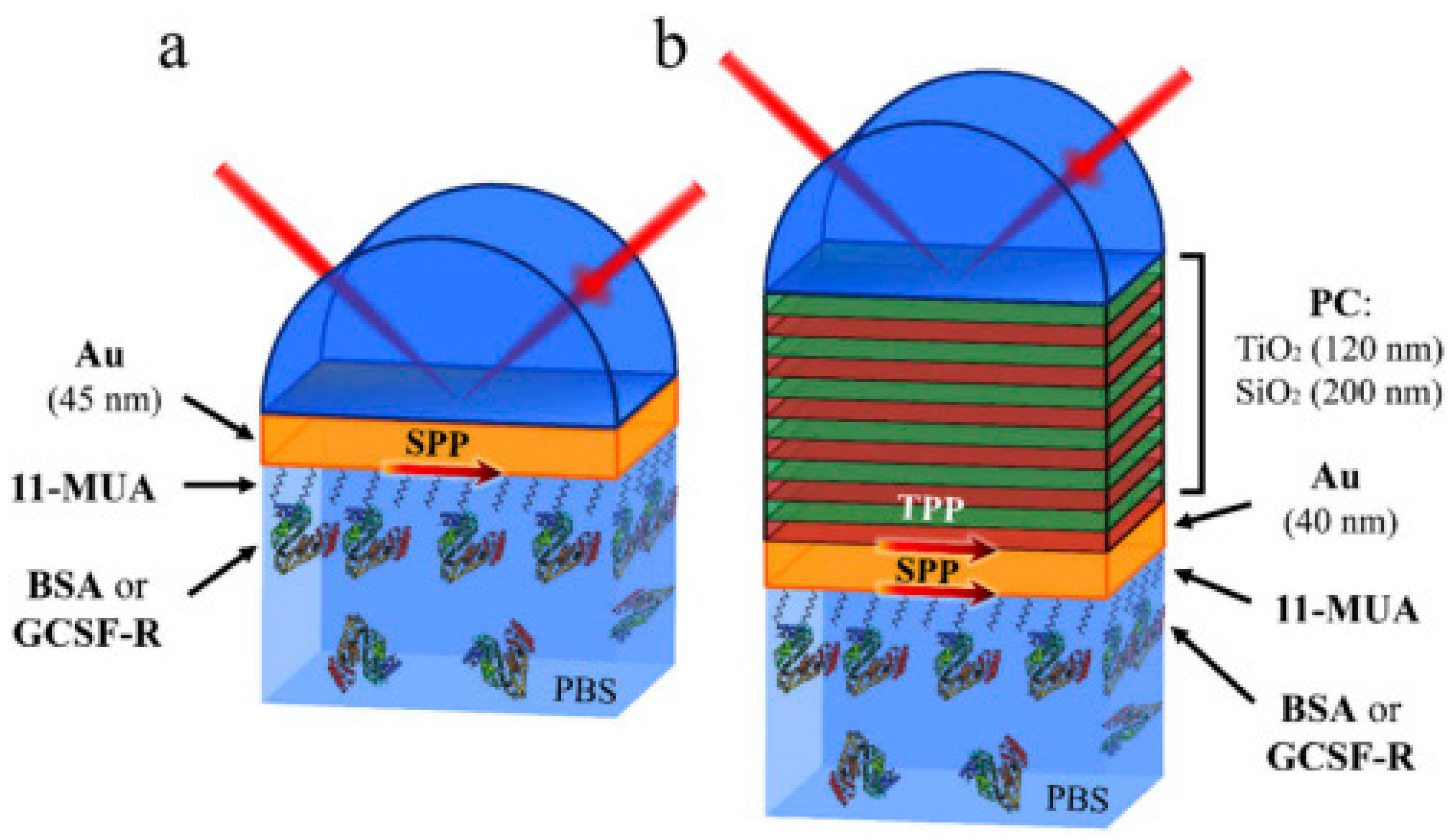
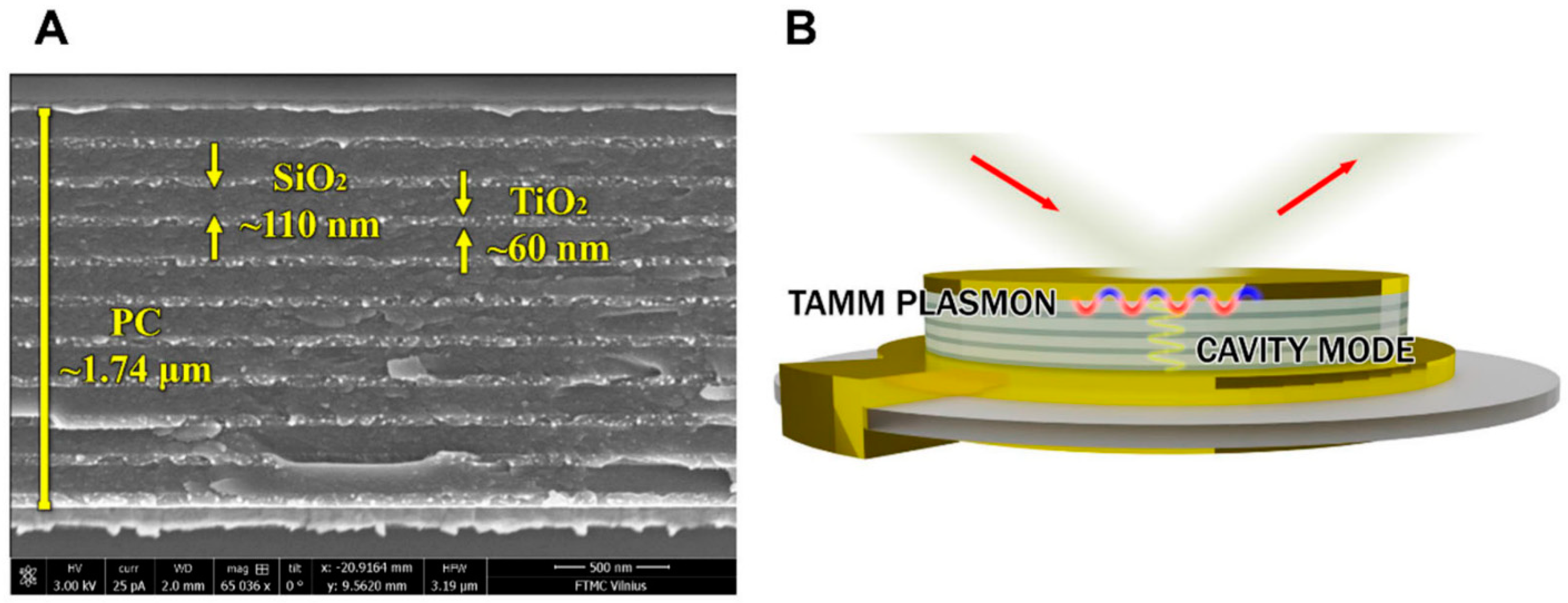
  105. Buzavaite-Verteliene, E.; Plikusiene, I.; Tolenis, T.; Valavicius, A.; Anulyte, J.; Ramanavicius, A.; Balevicius, Z. Hybrid Tamm-surface plasmon polariton mode for highly sensitive detection of protein interactions. Opt. Express 2020, 28, 29033. [Google Scholar] [CrossRef]
  106. Plikusienė, I.; Bužavaitė-Vertelienė, E.; Mačiulis, V.; Valavičius, A.; Ramanavičienė, A.; Balevičius, Z. Application of tamm plasmon polaritons and cavity modes for biosensing in the combined spectroscopic ellipsometry and quartz crystal microbalance method. Biosensors 2021, 11, 501. [Google Scholar] [CrossRef]
  107. Pal, A.K.; Pagal, S.; Prashanth, K.; Chandra, G.K.; Umapathy, S.; Mohan, D.B. Ag/ZnO/Au 3D hybrid structured reusable SERS substrate as highly sensitive platform for DNA detection. Sens. Actuators B Chem. 2019, 279, 157–169. [Google Scholar] [CrossRef]
  108. Kim, D.-K.; Kim, D.M.; Yoo, S.M.; Lee, S.Y. Controllable gold-capped nanoporous anodic alumina chip for label-free, specific detection of bacterial cells. RSC Adv. 2017, 7, 18815–18820. [Google Scholar] [CrossRef] [Green Version]
  109. Plikusiene, I.; Balevicius, Z.; Ramanaviciene, A.; Talbot, J.; Mickiene, G.; Balevicius, S.; Stirke, A.; Tereshchenko, A.; Tamosaitis, L.; Zvirblis, G.; et al. Evaluation of affinity sensor response kinetics towards dimeric ligands linked with spacers of different rigidity: Immobilized recombinant granulocyte colony-stimulating factor based synthetic receptor binding with genetically engineered dimeric analyte d. Biosens. Bioelectron. 2020, 156, 112112. [Google Scholar] [CrossRef]
  110. Balevicius, Z.; Talbot, J.; Tamosaitis, L.; Plikusiene, I.; Stirke, A.; Mickiene, G.; Balevicius, S.; Paulauskas, A.; Ramanavicius, A. Modelling of immunosensor response: The evaluation of binding kinetics between an immobilized receptor and structurally-different genetically engineered ligands. Sens. Actuators B Chem. 2019, 297, 126770. [Google Scholar] [CrossRef]
  111. Plikusiene, I.; Maciulis, V.; Ramanaviciene, A.; Balevicius, Z.; Buzavaite-Verteliene, E.; Ciplys, E.; Slibinskas, R.; Simanavicius, M.; Zvirbliene, A.; Ramanavicius, A. Evaluation of kinetics and thermodynamics of interaction between immobilized SARS-CoV-2 nucleoprotein and specific antibodies by total internal reflection ellipsometry. J. Colloid Interface Sci. 2021, 594, 195–203. [Google Scholar] [CrossRef]
  112. Plikusiene, I.; Maciulis, V.; Juciute, S.; Maciuleviciene, R.; Balevicius, S.; Ramanavicius, A.; Ramanaviciene, A. Investigation and Comparison of Specific Antibodies’ Affinity Interaction with SARS-CoV-2 Wild-Type, B.1.1.7, and B.1.351 Spike Protein by Total Internal Reflection Ellipsometry. Biosensors 2022, 12, 351. [Google Scholar] [CrossRef]
  113. Stetter, J.R.; Penrose, W.R. Understanding Chemical Sensors and Chemical Sensor Arrays (Electronic Noses): Past, Present, and Future. Sens. Update 2002, 10, 189–229. [Google Scholar] [CrossRef]
  114. Yang, J.; Cho, M.; Lee, Y. Synthesis of hierarchical Ni(OH)2 hollow nanorod via chemical bath deposition and its glucose sensing performance. Sens. Actuators B Chem. 2016, 222, 674–681. [Google Scholar] [CrossRef]
  115. Kim, E.B.; Seo, H.K. Highly sensitive formaldehyde detection using well-aligned zinc oxide nanosheets synthesized by chemical bath deposition technique. Materials 2019, 12, 250. [Google Scholar] [CrossRef] [Green Version]
  116. Kaur, N.; Raj, P.; Singh, A.; Singh, N.; Kim, D.Y. A facile route to ionic liquids-functionalized ZnO nanorods for the fluorometric sensing of thiabendazole drug. J. Mol. Liq. 2018, 261, 137–145. [Google Scholar] [CrossRef]
  117. Shariati, R.; Rezaei, B.; Jamei, H.R.; Ensafi, A.A. Application of coated green source carbon dots with silica molecularly imprinted polymers as a fluorescence probe for selective and sensitive determination of phenobarbital. Talanta 2019, 194, 143–149. [Google Scholar] [CrossRef]
  118. Shetti, N.P.; Malode, S.J.; Nayak, D.S.; Aminabhavi, T.M.; Reddy, K.R. Nanostructured silver doped TiO2/CNTs hybrid as an efficient electrochemical sensor for detection of anti-inflammatory drug, cetirizine. Microchem. J. 2019, 150, 104124. [Google Scholar] [CrossRef]
  119. Yadav, M.; Dhanda, M.; Arora, R.; Jagdish, R.; Singh, G.; Lata, S. Titania (TiO2)/silica (SiO2) nanospheres or NSs amalgamated on a pencil graphite electrode to sense l-ascorbic acid electrochemically and augmented NSs for antimicrobial behaviour. New J. Chem. 2022, 46, 12783–12796. [Google Scholar] [CrossRef]
  120. Xiao, W.; Ding, L.; He, J.; Huang, J. Preparation of lucigenin-doped silica nanoparticles and their application in fiber optic chloride ion sensor. Opt. Mater. (Amst.) 2019, 98, 109467. [Google Scholar] [CrossRef]
  121. Alam, M.M.; Rahman, M.M.; Uddin, M.T.; Asiri, A.M.; Chani, M.T.S.; Islam, M.A. Development of L-glutamic acid biosensor with ternary ZnO/NiO/Al2O3 nanoparticles. J. Lumin. 2020, 227, 117528. [Google Scholar] [CrossRef]
  122. Rahman, M.M.; Ahmed, J.; Asiri, A.M.; Alamry, K.A. Fabrication of a hydrazine chemical sensor based on facile synthesis of doped NZO nanostructure materials. New J. Chem. 2020, 44, 13018–13029. [Google Scholar] [CrossRef]
  123. Hu, J.; Zhang, M.; Wang, X.; Sun, Y.; Li, P.; Zhang, W.; Lian, K.; Chen, L.; Chen, Y. Synthesis and characterization of flower-like MoO3/In2O3 microstructures for highly sensitive ethanol detection. RSC Adv. 2017, 7, 23478–23485. [Google Scholar] [CrossRef]
Figure 1. Synthesis methods of various nanostructures and their application in different sensors design.
Nanomaterials 12 04413 g001
Figure 2. Scheme for total synthesis of dendrimer encapsulated mesoporous silica NPs. Step (1) inoculation of dendrimer with metal ions, (2) formation of reverse microemulsion with disperse phase (blue) and continuous phase (orange), (3) base catalyzed silica formation, and (4) acid catalyzed etching of metal encapsulated dendrimers. Adapted from [45].
Nanomaterials 12 04413 g002
Figure 3. (a) Schematic synthesis diagram of the 3D flower-like hierarchical ZnO microstructures; (b) SEM image of as-grown MFs; (c) SEM image of a single MF and corresponding EDX elemental maps. Adapted from [56].
Nanomaterials 12 04413 g003
Figure 4. Scheme of the fabrication of immunosensor with a sandwich configuration based on ZnO nanorods. Adapted from [67].
Nanomaterials 12 04413 g004
Figure 5. Scheme showing the synthetic process to generate (a) ZnO@ZIF-8-x-y and Co(CO3)0.5(OH)·0.11H2O@ZIF-67-x-y using 2-Melm vapor, where x and y are the synthesis temperature and synthesis time, respectively. (b) Advantages of Co3O4/NC hybrid materials. Adapted from [34], 2018, American Chemical Society.
Nanomaterials 12 04413 g005
Figure 6. Four different dimensions of ZnO nanostructures with their advantages. Zero-dimensional nanostructures provide a large surface area. One-dimensional nanostructures possess stable and direct electron transport. Two-dimensional nanostructures give specific planes for immobilization process for the simultaneous detection of different analytes. Three-dimensional nanostructures have extra surface area (outer and inner area) to provide more sites for immobilization. Adopted from [27].
Nanomaterials 12 04413 g006
Figure 7. Total internal reflection geometry schematic of the Au (a) and PC/Au (b) samples with a self-assembled monolayer of 11-mercaptoundecanoic acid (11-MUA) and the GCSF-R or BSA protein in phosphate-buffered saline solution. Adopted from [105].
Nanomaterials 12 04413 g007
Figure 8. SEM micrograph of the plasmonic photonic structure modified QCM-D sensor chip (A) and Tamm plasmons and cavity mode excitation using nanometer structures of formed photonic crystal (B). Adopted from [106].
Nanomaterials 12 04413 g008
Table 1. Nanostructure formation methods, detected analyte and reported biosensing properties.
NanostructureMethod of
Synthesis
ApplicationReported Sensing
Properties
Ref.
ZnO nanostructuresChemical bath depositionElectrochemical immunosensor for ZIKV-NS1 antigenLOD: 1.00 pg/mL
LDR: 0.1–100 ng/mL
[100]
MoS2/Cu2OChemical vapour deposition, electrodepositionGSH, GSSG biosensor for indirect cancer cell detectionLDR: 0–50,000 cells[101]
Au(Fe3O4) MNPsCo-precipitation, wet chemicalColorimetric hGH sensorLOD: 0.082 nM
LDR: 0.1–5.0 nM
[102]
Au(Fe3O4) MNPsCo-precipitation, wet chemicalSPR CD5 immunosensorLOD: 8.31 fM[103]
ZnO NRs-rGOElectrodepositionElectrochemical IgG detectionLOD: 1.25 ng/mL
LDR: 10–1000 ng/mL
[67]
ZnO NWLsElectrodepositionElectrochemical enzymatic H2O2 sensor for cancer cell detectionLOD: 0.8 μM
LDR: 1–1000 μM
[104]
Au/(TiO2/SiO2)
Photonic crystal
Ion beam
sputtering
TIRE signal enhancement6.4 times more sensitive than SPR[105]
Au/(TiO2/SiO2)/AuIon beam
sputtering
SE/QCM-D signal enhancement23 and 49 times increased SE signal[106]
Ag/ZnO-NRs/AuThermal evaporation; hydrothermal; sputteringSERS sensing platformLOD (λ-DNA): 10 ng/μL
LOD (Rh6G): 10−16 M
[107]
Au/PAATwo-step anodization; thermal evaporationInterferometric aptamer based bacterial cell sensorLOD: 20 CFU/mL
LDR: 103–109 CFU/mL
[108]
Abbreviations: ZIKV-NS1—Zika virus NS1 antigen, LOD—limit of detection, LDR—linear dynamic range, GSH—glutathione, GSSG—glutathione disulphide, MNP—magnetic nanoparticle, hGH—human growth hormone, SPR—surface plasmon resonance, CD5—lymphocyte antigen T1, NRs—nanorods, rGO—reduced graphene, IgG—Immunoglobulin G, NWLs—nanowalls, TIRE—total internal reflection ellipsometry, SE—spectroscopic ellipsometry, QCM-D—quartz crystal microbalance with dissipation, SERS—surface enhanced Raman spectroscopy, Rh6G—Rhodamine—6 G, PAA—porous anodic alumina, CFU—colony forming unit.
Table 2. Nanostructure formation methods, detected analyte, and reported chemical sensing properties.
NanostructureMethod of
Synthesis
ApplicationReported Sensing
Properties
Ref.
Ni(OH)2 HRsChemical bath depositionElectrochemical glucose sensorLOD: 0.6 μM
LDR: 0.002–3.8 mM
[114]
ZnO NSsChemical bath depositionElectrochemical aqueous formaldehyde sensorLOD: 210 nM[115]
ZnO NRsHydrothermalFluorescence thiabendazole sensorLOD: 304 nM
LDR: 10–80 μM
[116]
SiO2/GSCDsHydrothermal, reverse microemulsionFluorescence phenobarbital sensorLOD: 0.1 nM
LDR: 0.4–34.5 nM
[117]
Ag-TiO2 NPs/MWCNTsHydrothermal, powder blendingElectrochemical cetirizine sensorLOD: 8.76 nM
LDR: 0.3–3 μM
[118]
TiO2@SiO2 NSsSol-gelElectrochemical ascorbic acid sensorLOD: 383.3 μM
LDR: 50–2500 μM
[119]
Lucigenin doped SiO2 NPsReverse microemulsionFibre optic Cl sensorLDR: 0.02–0.06 M[120]
ZnO/NiO/Al2O3 NPsWet chemicalElectrochemical L-glutamic acid sensorLOD: 95.35 pM
LDR: 0.1 nM–0.01 mM
[121]
Ni-ZnO NPsWet chemicalElectrochemical hydrazine sensorLOD: 1.7 pM
LDR: 0.2 nM–0.02 M
[122]
Abbreviations: HRs—hollow rods, LOD—limit of detection, LDR—linear dynamic range, NS—nanosheets, GSCDs—green source carbon dots, NPs—nanoparticles, MWCNTs—multi-walled carbon nanotubes.
Publisher’s Note: MDPI stays neutral with regard to jurisdictional claims in published maps and institutional affiliations.

