
Submicron-Size Emitters of the 1.2–1.55 μm Spectral Range Based on InP/InAsP/InP Nanostructures Integrated into Si Substrate

 , , , , and
Abstract
1. Introduction
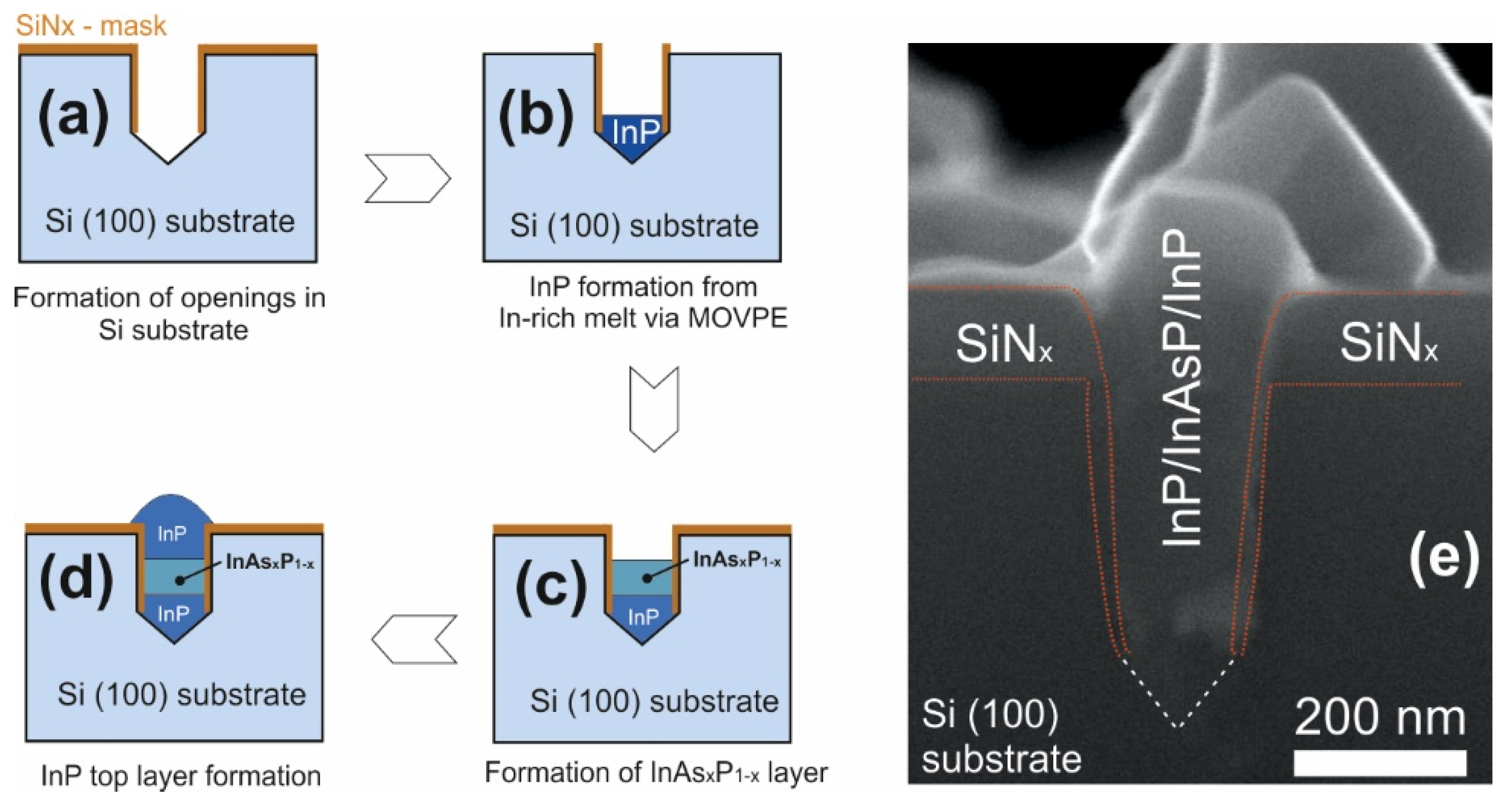
2. Materials and Methods
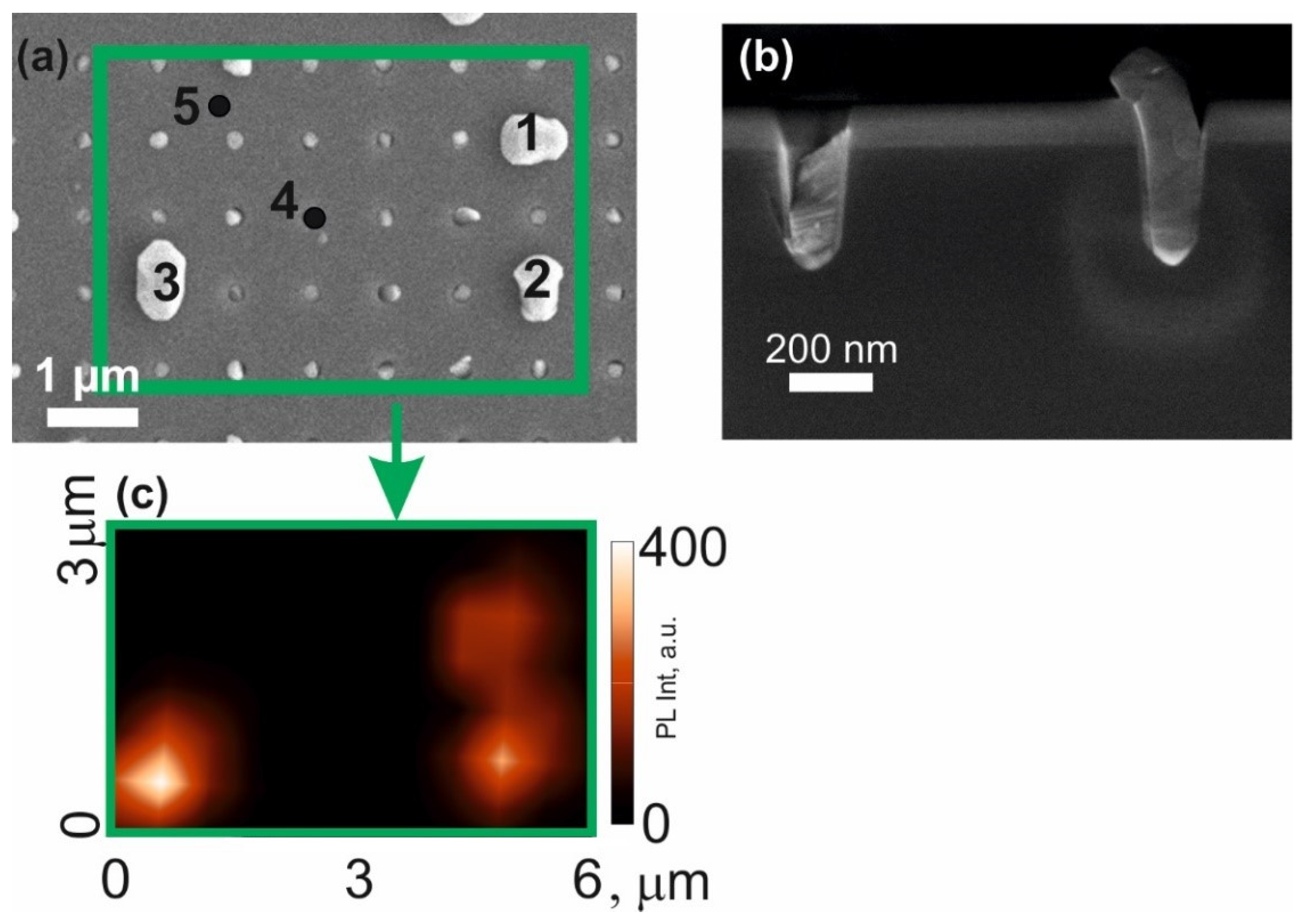
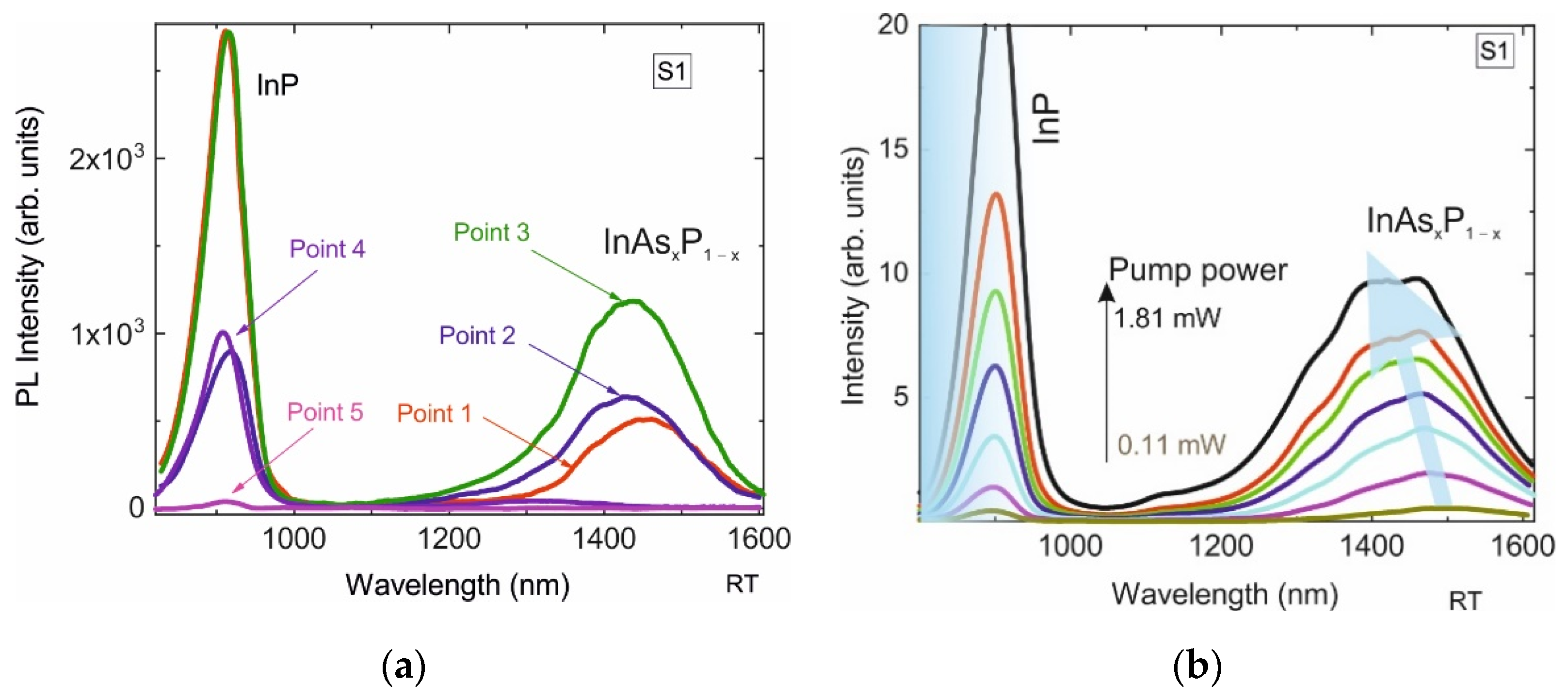
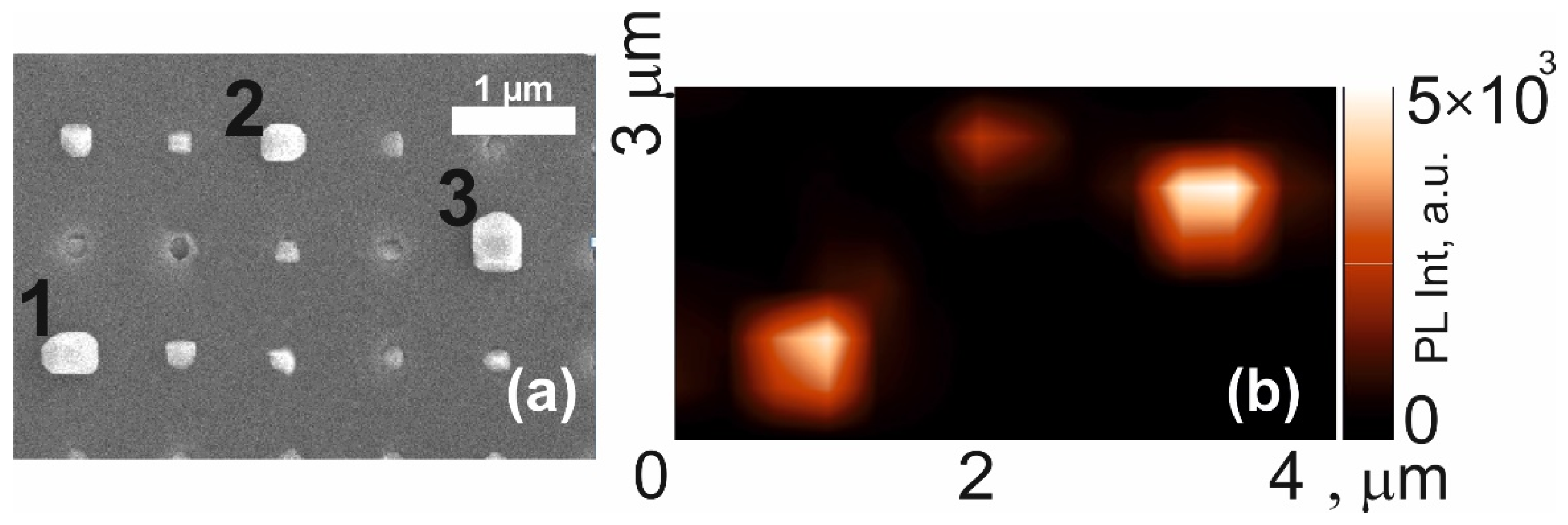
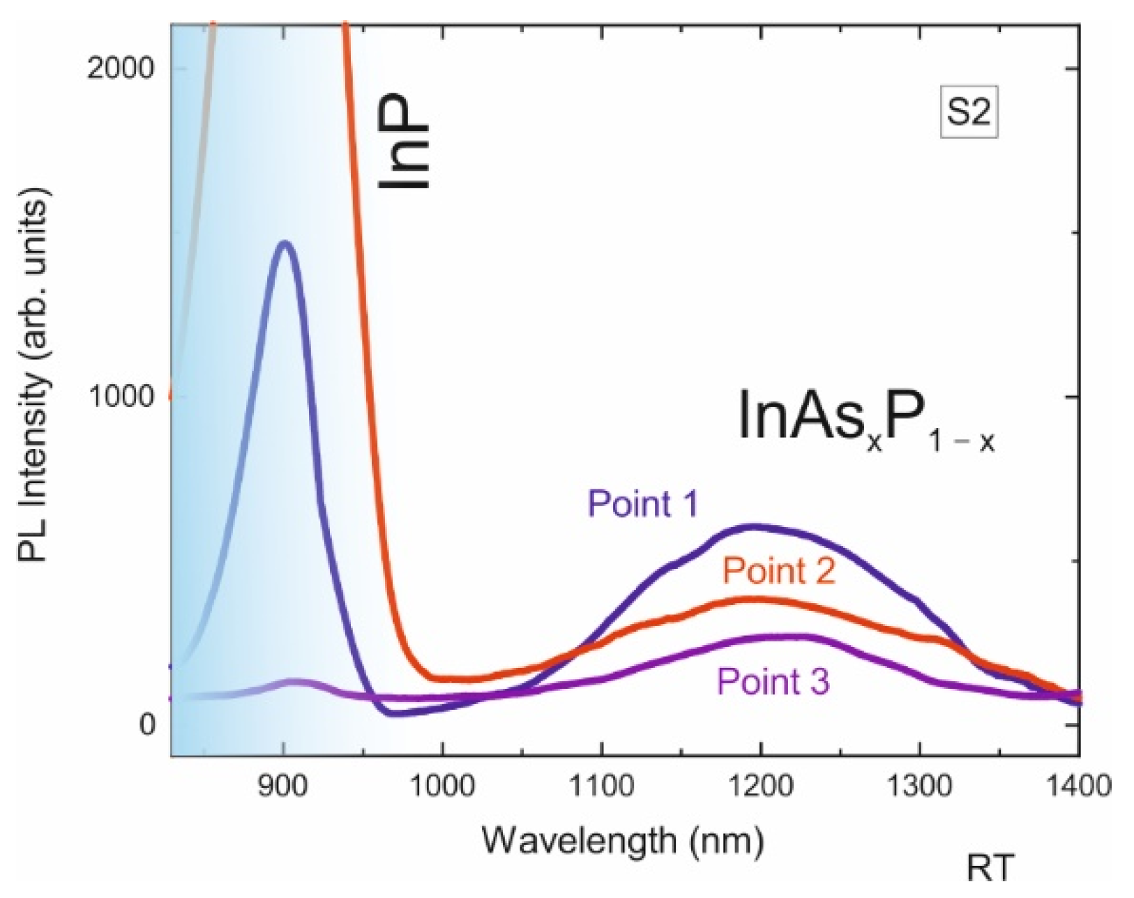
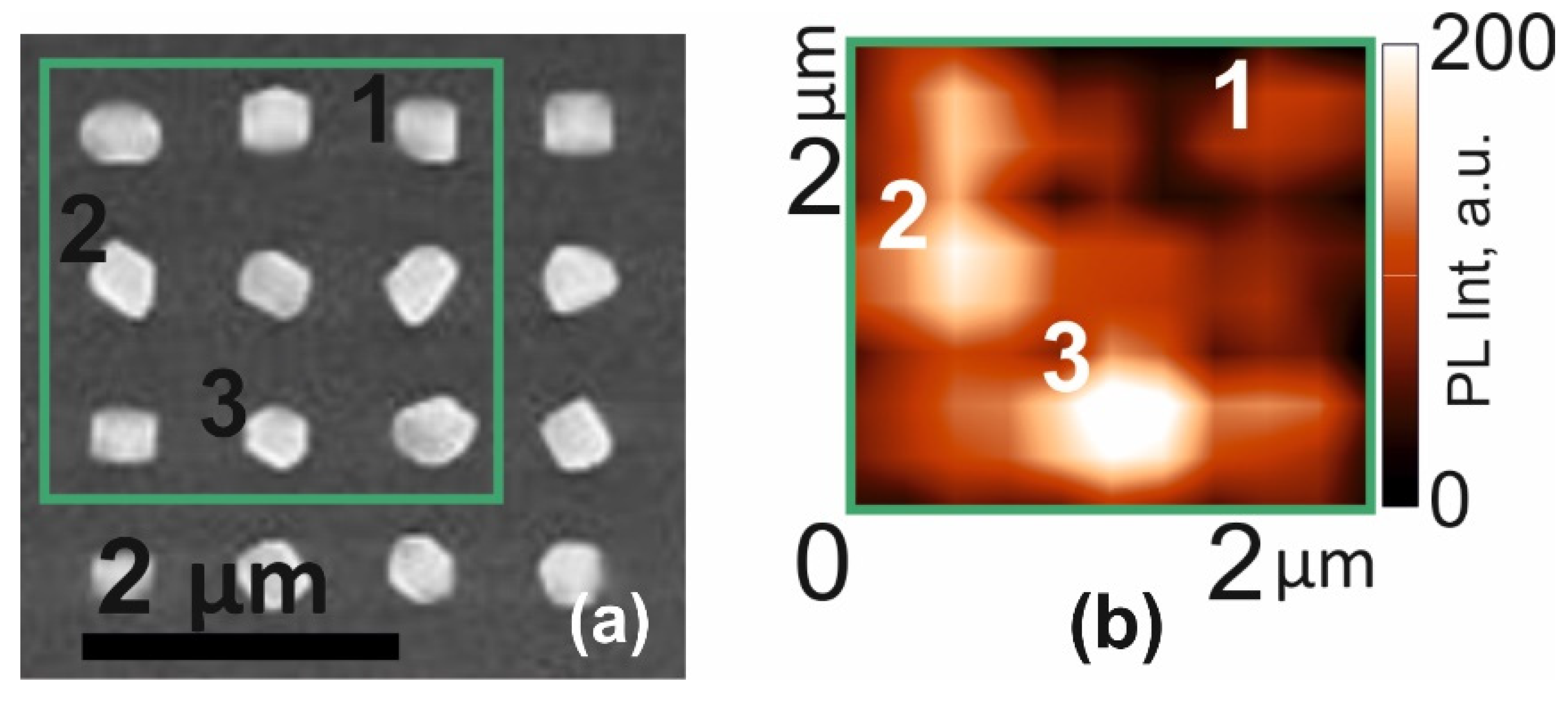
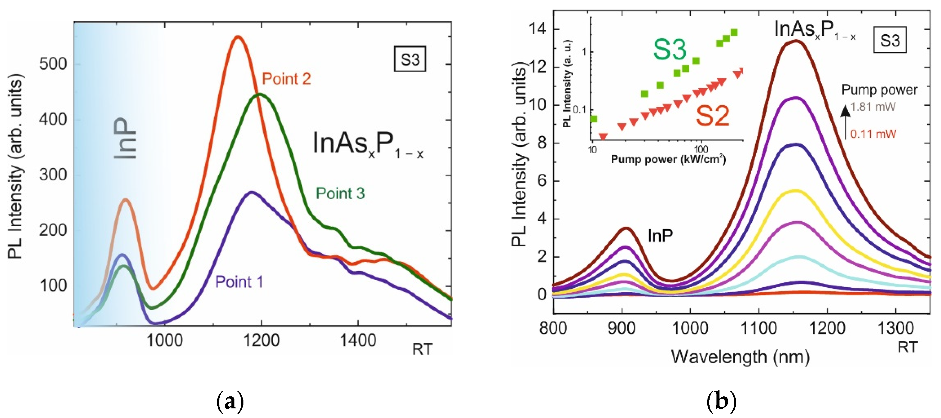
3. Results and Discussion
4. Conclusions
Author Contributions
Funding
Institutional Review Board Statement
Informed Consent Statement
Data Availability Statement
Conflicts of Interest
References
- Elshaari, A.W.; Pernice, W.; Srinivasan, K.; Benson, O.; Zwiller, V. Hybrid integrated quantum photonic circuits. Nat. Photonics 2020, 14, 285–298. [Google Scholar] [CrossRef] [PubMed]
- Liao, M.; Chen, S.; Park, J.-S.; Seeds, A.; Liu, H. III–V quantum-dot lasers monolithically grown on silicon. Semicond. Sci. Technol. 2018, 33, 123002. [Google Scholar] [CrossRef]
- Yu, Y.; Xue, W.; Semenova, E.; Yvind, K.; Mork, J. Demonstration of a self-pulsing photonic crystal Fano laser. Nat. Photonics 2017, 11, 81–84. [Google Scholar] [CrossRef]
- Aharonovich, I.; Englund, D.; Toth, M. Solid-state single-photon emitters. Nat. Photonics 2016, 10, 631–641. [Google Scholar] [CrossRef]
- Park, G.C.; Xue, W.; Piels, M.; Zibar, D.; Mørk, J.; Semenova, E.; Chung, I.-S. Ultrahigh-speed Si-integrated on-chip laser with tailored dynamic characteristics. Sci. Rep. 2016, 6, 38801. [Google Scholar] [CrossRef]
- Waldron, N.; Merckling, C.; Teugels, L.; Ong, P.; Ibrahim, S.A.U.; Sebaai, F.; Pourghaderi, A.; Barla, K.; Collaert, N.; Thean, A.V.-Y. InGaAs Gate-All-Around Nanowire Devices on 300mm Si Substrates. IEEE Electron. Device Lett. 2014, 35, 1097–1099. [Google Scholar] [CrossRef]
- Borg, M.; Schmid, H.; Moselund, K.E.; Signorello, G.; Gignac, L.; Bruley, J.; Breslin, C.; Das Kanungo, P.; Werner, P.; Riel, H. Vertical III–V Nanowire Device Integration on Si(100). Nano Lett. 2014, 14, 1914–1920. [Google Scholar] [CrossRef]
- Kunert, B.; Mols, Y.; Baryshniskova, M.; Waldron, N.; Schulze, A.; Langer, R. How to control defect formation in monolithic III/V hetero-epitaxy on (100) Si? A critical review on current approaches. Semicond. Sci. Technol. 2018, 33, 093002. [Google Scholar] [CrossRef]
- Wan, Y.; Norman, J.C.; Tong, Y.; Kennedy, M.J.; He, W.; Selvidge, J.; Shang, C.; Dumont, M.; Malik, A.; Tsang, H.K.; et al. 1.3 μm Quantum Dot-Distributed Feedback Lasers Directly Grown on (001) Si Laser. Photon. Rev. 2020, 14, 2000037. [Google Scholar]
- Wan, Y.; Zhang, S.; Norman, J.C.; Kennedy, M.J.; He, W.; Liu, S.; Xiang, C.; Shang, C.; He, J.-J.; Gossard, A.C.; et al. Quantum dot lasers grown directly on silicon. Optica 2019, 6, 1394. [Google Scholar] [CrossRef]
- Luxmoore, I.J.; Toro, R.; Zamudio, O.D.P.; Wasley, N.A.; Chekhovich, E.A.; Sanchez, A.; Beanland, R.; Fox, A.M.; Skolnick, M.; Liu, H.Y.; et al. III-V quantum light source and cavity-QED on silicon. Sci. Rep. 2013, 3, 1239. [Google Scholar] [CrossRef] [PubMed]
- Daix, N.; Uccelli, E.; Czornomaz, L.; Caimi, D.; Rossel, C.; Sousa, M.; Siegwart, H.; Marchiori, C.; Hartmann, J.M.; Shiu, K.-T.; et al. Towards large size substrates for III-V co-integration made by direct wafer bonding on Si. APL Mater. 2014, 2, 086104. [Google Scholar] [CrossRef]
- Widiez, J.; Sollier, S.; Baron, T.; Martin, M.; Gaudin, G.; Mazen, F.; Madeira, F.; Favier, S.; Salaun, A.; Alcotte, R.; et al. 300 mm InGaAs-on-insulator substrates fabricated using direct wafer bonding and the Smart Cut(TM) technology. Jpn. J. Appl. Phys. 2016, 55, 04EB10. [Google Scholar] [CrossRef]
- Sahoo, H.K.; Ottaviano, L.; Zheng, Y.; Hansen, O.; Yvind, K. Low temperature bonding of heterogeneous materials using Al2O3 as an intermediate layer. J. Vac. Sci. Technol. B 2018, 36, 011202. [Google Scholar] [CrossRef]
- Sakanas, A.; Semenova, E.; Ottaviano, L.; Mørk, J.; Yvind, K. Comparison of processing-induced deformations of InP bonded to Si determined by e-beam metrology: Direct vs. adhesive bonding. Microelectron. Eng. 2019, 214, 93–99. [Google Scholar] [CrossRef]
- Mauthe, S.; Vico Trivino, N.; Baumgartner, Y.; Sousa, M.; Caimi, D.; Stoferle, T.; Schmid, H.; Moselund, K.E. InP-on-Si Optically Pumped Microdisk Lasers via Monolithic Growth and Wafer Bonding. IEEE J. Sel. Top. Quantum Electron. 2019, 25, 1–7. [Google Scholar] [CrossRef]
- Merckling, C.; Waldron, N.; Jiang, S.; Guo, W.; Barla, K.; Heyns, M.; Collaert, N.; Thean, A.; Vandervorst, W. Selective-Area Metal Organic Vapor-Phase Epitaxy of III-V on Si: What About Defect Density? ECS Trans. 2014, 64, 513–521. [Google Scholar] [CrossRef]
- Wang, Z.; Tian, B.; Pantouvaki, M.; Guo, W.; Absil, P.; Van Campenhout, J.; Merckling, C.; Van Thourhout, D. Roomtemperature InP distributed feedback laser array directly grown on silicon. Nat. Photonics 2015, 9, 837–842. [Google Scholar] [CrossRef]
- Niu, G.; Capellini, G.; Hatami, F.; Di Bartolomeo, A.; Niermann, T.; Hussein, E.H.; Schubert, M.A.; Krause, H.-M.; Zaumseil, P.; Skibitzki, O.; et al. Selective Epitaxy of InP on Si and Rectification in Graphene/InP/Si Hybrid Structure. ACS Appl. Mater. Interfaces 2016, 8, 26948–26955. [Google Scholar] [CrossRef]
- Iemmo, L.; Di Bartolomeo, A.; Giubileo, F.; Luongo, G.; Passacantando, M.; Niu, G.; Hatami, F.; Skibitzki, O.; Schroeder, T. Graphene enhanced field emission from InP nanocrystals. Nanotechnology 2017, 28, 495705. [Google Scholar] [CrossRef]
- Vukajlovic-Plestina, J.; Kim, W.; Ghisalberti, L.; Varnavides, G.; Tütüncuoglu, G.; Potts, H.; Friedl, M.; Güniat, L.; Carter, W.C.; Dubrovskii, V.G.; et al. Fundamental aspects to localize self-catalyzed III-V nanowires on silicon. Nat. Commun. 2019, 10, 869. [Google Scholar] [CrossRef] [PubMed]
- Bollani, M.; Bietti, S.; Frigeri, C.; Chrastina, D.; Reyes, K.; Smereka, P.; Millunchick, J.M.; Vanacore, G.M.; Burghammer, M.; Tagliaferri, A.; et al. Ordered arrays of embedded Ga nanoparticles on patterned silicon substrates. Nanotechnology 2014, 25, 205301. [Google Scholar] [CrossRef] [PubMed]
- Oehler, F.; Cattoni, A.; Scaccabarozzi, A.; Patriarche, G.; Glas, F.; Harmand, J.C. Measuring and Modeling the Growth Dynamics of Self-Catalyzed GaP Nanowire Arrays. Nano Lett. 2018, 18, 701–708. [Google Scholar] [CrossRef]
- Mayer, B.F.; Wirths, S.; Mauthe, S.; Staudinger, P.; Sousa, M.; Winiger, J.; Schmid, H.; Moselund, K.E. Microcavity Lasers on Silicon by Template-Assisted Selective Epitaxy of Microsubstrates. IEEE Photonics Technol. Lett. 2019, 31, 1021–1024. [Google Scholar] [CrossRef]
- Herranz, J.; Corfdir, P.; Luna, E.; Jahn, U.; Lewis, R.B.; Schrottke, L.; Lähnemann, J.; Tahraoui, A.; Trampert, A.; Brandt, O.; et al. Coaxial GaAs/(In,Ga)As Dot-in-a-Well Nanowire Heterostructures for Electrically Driven Infrared Light Generation on Si in the Telecommunication O Band. ACS Appl. Nano Mater. 2020, 3, 165–174. [Google Scholar] [CrossRef]
- Kunert, B.; Guo, W.; Mols, Y.; Tian, B.; Wang, Z.; Shi, Y.; Van Thourhout, D.; Pantouvaki, M.; Van Campenhout, J.; Langer, R.; et al. III/V nano ridge structures for optical applications on patterned 300 mm silicon substrate. Appl. Phys. Lett. 2016, 109, 091101. [Google Scholar] [CrossRef]
- Güniat, L.; Caroff, P.; Fontcuberta i Morral, A. Vapor Phase Growth of Semiconductor Nanowires: Key Developments and Open Questions. Chem. Rev. 2019, 119, 8958–8971. [Google Scholar] [CrossRef] [PubMed]
- Yuan, X.; Pan, D.; Zhou, Y.; Zhang, X.; Peng, K.; Zhao, B.; Deng, M.; He, J.; Tan, H.H.; Jagadish, C. Selective area epitaxy of III–V nanostructure arrays and networks: Growth, applications, and future directions. Appl. Phys. Rev. 2021, 8, 021302. [Google Scholar] [CrossRef]
- Chang, T.-Y.; Kim, H.; Hubbard, W.A.; Azizur-Rahman, K.M.; Ju, J.J.; Kim, J.-H.; Lee, W.-J.; Huffaker, D. InAsP Quantum Dot-Embedded InP Nanowires toward Silicon Photonic Applications. ACS Appl. Mater. Interfaces 2022, 14, 12488–12494. [Google Scholar] [CrossRef]
- Viazmitinov, D.V.; Berdnikov, Y.; Kadkhodazadeh, S.; Dragunova, A.; Sibirev, N.; Kryzhanovskaya, N.; Radko, I.; Huck, A.; Yvind, K.; Semenova, E. Monolithic integration of InP on Si by molten alloy driven selective area epitaxial growth. Nanoscale 2020, 12, 23780–23788. [Google Scholar] [CrossRef]
- Saenz, T.E.; McMahon, W.E.; Norman, A.G.; Perkins, C.L.; Zimmerman, J.D.; Warren, E.L. High-Temperature Nucleation of GaP on V-Grooved Si. Cryst. Growth Des. 2020, 20, 6745–6751. [Google Scholar] [CrossRef]
- Dargys, A.; Kundrotas, J. Handbook on Physical Properties of Ge, Si, GaAs and InP; Science and Encyclopedia Publishers: Vilnius, Lithuania, 1994. [Google Scholar]
- Vurgaftman, I.; Meyer, J.R.; Ram-Mohan, L.R. Band parameters for III–V compound semiconductors and their alloys. J. Appl. Phys. 2001, 89, 5815. [Google Scholar] [CrossRef]
- Dmitriev, D.V.; Kolosovsky, D.A.; Fedosenko, E.V.; Toropov, A.I.; Zhuravlev, K.S. Substitution of Phosphorus at the InP(001) Surface Upon Annealing in an Arsenic Flux. Semiconductors 2021, 55, 823–827. [Google Scholar] [CrossRef]
- Akahane, K.; Matsumoto, A.; Umezawa, T.; Yamamoto, N. Fabrication of In(P)As Quantum Dots by Interdiffusion of P and As on InP(311)B Substrate. Crystals 2020, 10, 90. [Google Scholar] [CrossRef]


| Sample | Annealing Time under 175 sccm of AsH3 Flux | Number of InAsxP1−x Layers |
|---|---|---|
| S1 | 180 s | 1 |
| S2 | 60 s | 1 |
| S3 | 60 s | 5 |
Publisher’s Note: MDPI stays neutral with regard to jurisdictional claims in published maps and institutional affiliations. |
© 2022 by the authors. Licensee MDPI, Basel, Switzerland. This article is an open access article distributed under the terms and conditions of the Creative Commons Attribution (CC BY) license (https://creativecommons.org/licenses/by/4.0/).
Share and Cite
Melnichenko, I.; Moiseev, E.; Kryzhanovskaya, N.; Makhov, I.; Nadtochiy, A.; Kalyuznyy, N.; Kondratev, V.; Zhukov, A. Submicron-Size Emitters of the 1.2–1.55 μm Spectral Range Based on InP/InAsP/InP Nanostructures Integrated into Si Substrate. Nanomaterials 2022, 12, 4213. https://doi.org/10.3390/nano12234213
Melnichenko I, Moiseev E, Kryzhanovskaya N, Makhov I, Nadtochiy A, Kalyuznyy N, Kondratev V, Zhukov A. Submicron-Size Emitters of the 1.2–1.55 μm Spectral Range Based on InP/InAsP/InP Nanostructures Integrated into Si Substrate. Nanomaterials. 2022; 12(23):4213. https://doi.org/10.3390/nano12234213
Chicago/Turabian StyleMelnichenko, Ivan, Eduard Moiseev, Natalia Kryzhanovskaya, Ivan Makhov, Alexey Nadtochiy, Nikolay Kalyuznyy, Valeriy Kondratev, and Alexey Zhukov. 2022. "Submicron-Size Emitters of the 1.2–1.55 μm Spectral Range Based on InP/InAsP/InP Nanostructures Integrated into Si Substrate" Nanomaterials 12, no. 23: 4213. https://doi.org/10.3390/nano12234213
APA StyleMelnichenko, I., Moiseev, E., Kryzhanovskaya, N., Makhov, I., Nadtochiy, A., Kalyuznyy, N., Kondratev, V., & Zhukov, A. (2022). Submicron-Size Emitters of the 1.2–1.55 μm Spectral Range Based on InP/InAsP/InP Nanostructures Integrated into Si Substrate. Nanomaterials, 12(23), 4213. https://doi.org/10.3390/nano12234213