
FDTD Simulations of Shell Scattering in Au@SiO2 Core–Shell Nanorods with SERS Activity for Sensory Purposes

Abstract
:1. Introduction
2. Theoretical Model and Method
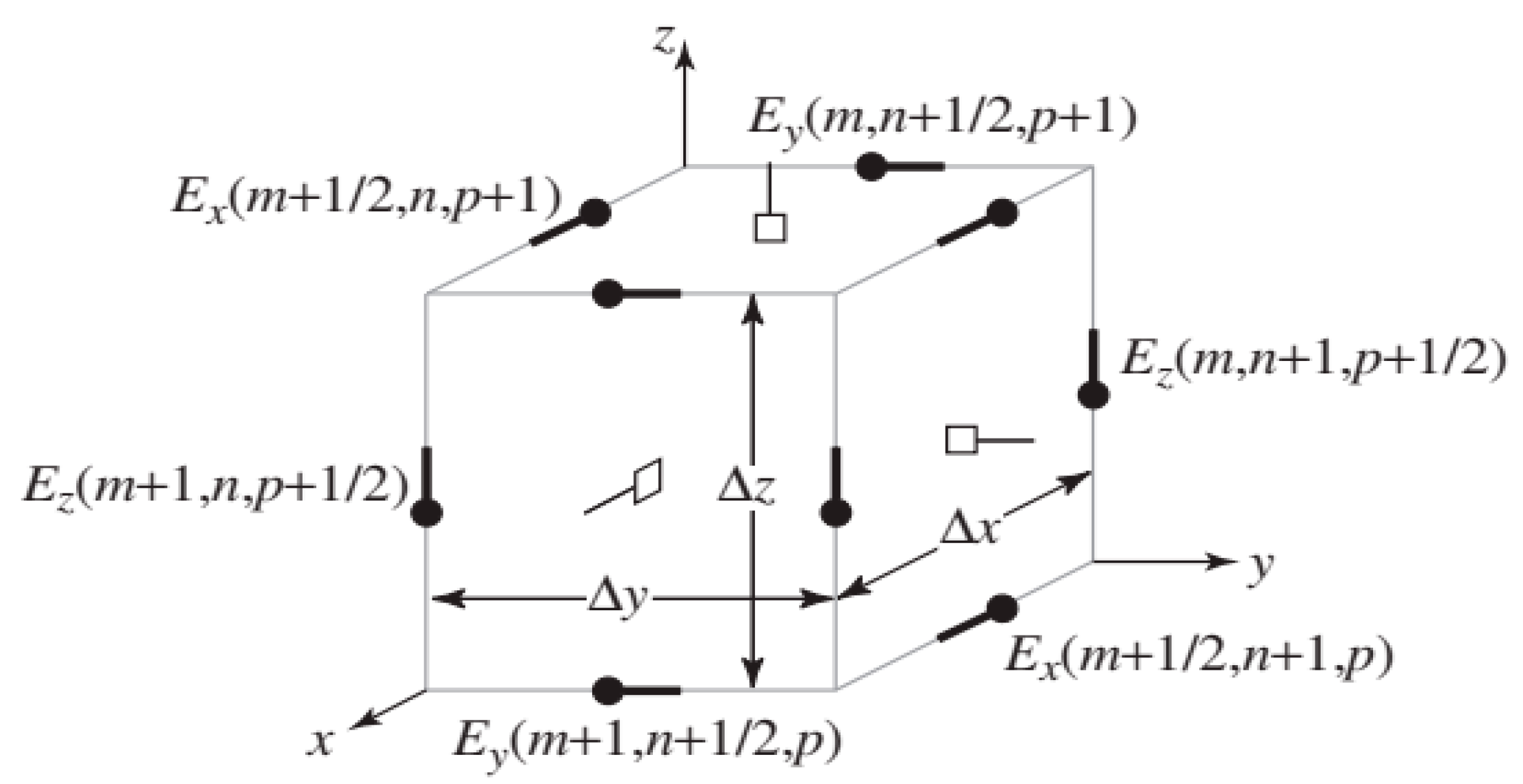
2.1. FDTD Approach
2.2. Raman Scattering and Enhancement Factor
2.3. Simulation Process
- −
- Layers (for PML area discretization purposes) = 8.
- −
- KAPPA, SIGMA, and ALPHA (absorptive properties of PML regions kappa, sigma, and alpha are estimated inside PML regions using polynomial functions) kappa = 2, sigma = 1, and alpha = 0.
- −
- Polynom (defines the order of the polynomial used to evaluate kappa and sigma) = 0.
- −
- Alpha-polynomial (defines the order of the polynomial used to evaluate the alpha channel) = 1.
- −
- Minimum and maximum layers (these provide an acceptable range of values for the number of PML layers). Minimum layers = 8 and maximum = 64.
- −
- Physical parameters of the simulation: travel time of a plane-polarized wave through the working area 1000 fs and temperature T = 300 °K.
3. Simulation Results and Discussion
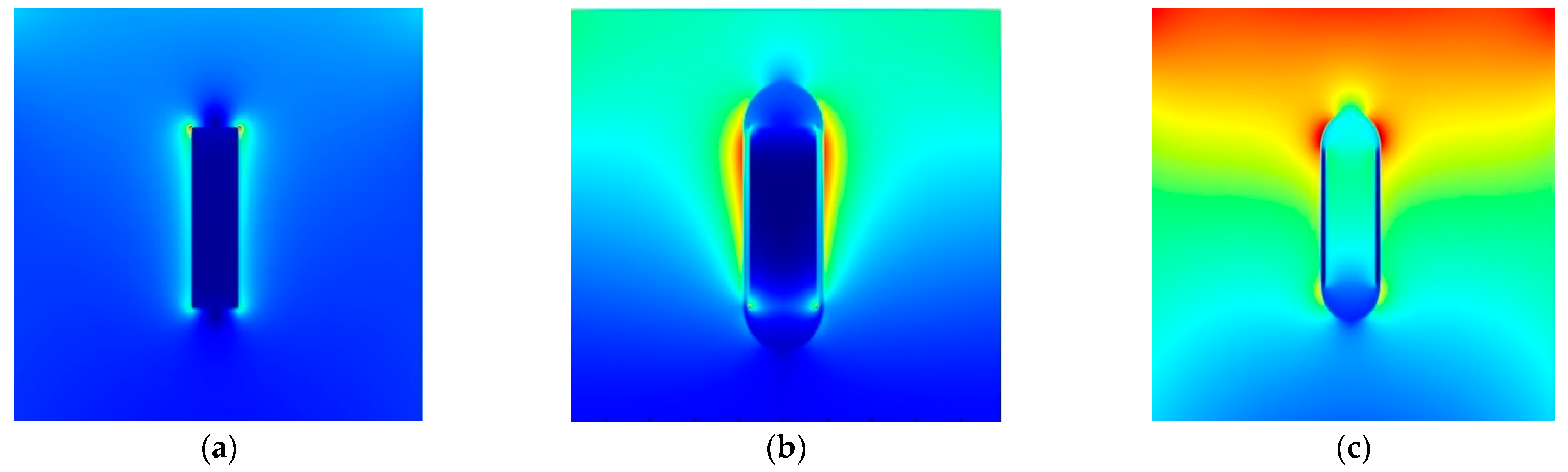
3.1. NR without a SiO2 Shell
3.2. NR with a SiO2 Shell
3.3. A Single (hollow) SiO2 Shell
3.4. Calculation of the Integral Sum for a Single (Hollow) SiO2 and NR Au@SiO2
4. Conclusions
Author Contributions
Funding
Institutional Review Board Statement
Informed Consent Statement
Data Availability Statement
Conflicts of Interest
References
- Razumova, M.; Lunga, Y.; Lozovski, V. Plasmonic Nanoparticles with Biospecific Surfaces in Optical Sensorics of BioLiquids. In Proceedings of the 2020 IEEE 40th International Conference on Electronics and Nanotechnology, Kyiv, Ukraine, 22–24 April 2020; pp. 415–418. [Google Scholar]
- Hanisch, C.; Kulkarni, A.; Zaporojtchenko, V.; Faupel, F. Polymer-metal nanocomposites with 2-dimensional Au nanoparticle arrays for sensoric applications. J. Phys. Conf. Ser. 2008, 100, 052043. [Google Scholar]
- Agafilushkina, S.N.; Žukovskaja, O.; Dyakov, S.A.; Weber, K.; Sivakov, V.; Popp, J.; Osminkina, L.A. Raman signal enhancement tunable by gold-covered porous silicon films with different morphology. Sensors 2020, 20, 5634. [Google Scholar] [CrossRef] [PubMed]
- Jazayeri, M.H.; Amani, H.; Pourfatollah, A.A.; Pazoki-Toroudi, H.; Sedighimoghaddam, B. Various methods of gold nanoparticles (GNPs) conjugation to antibodies. Sens. Bio-Sens. Res. 2016, 9, 17–22. [Google Scholar] [CrossRef] [Green Version]
- Mioc, A.; Mioc, M.; Ghiulai, R.; Voicu, M.; Racoviceanu, R.; Trandafirescu, C.; Soica, C. Gold nanoparticles as targeted delivery systems and theranostic agents in cancer therapy. Curr. Med. Chem. 2019, 26, 6493–6513. [Google Scholar] [CrossRef]
- Kim, C.K.; Ghosh, P.; Rotello, V.M. Multimodal drug delivery using gold nanoparticles. Nanoscale 2009, 1, 61–67. [Google Scholar] [CrossRef] [Green Version]
- Kang, B.; Yu, D.; Dai, Y.; Chang, S.; Chen, D.; Ding, Y. Biodistribution and accumulation of intravenously administered carbon nanotubes in mice probed by Raman spectroscopy and fluorescent labeling. Carbon 2009, 47, 1189–1192. [Google Scholar] [CrossRef]
- Pramanik, A.K.; Palanimuthu, D.; Somasundaram, K.; Samuelson, A.G. Biotin decorated gold nanoparticles for targeted delivery of a smart-linked anticancer active copper complex: In vitro and in vivo studies. Bioconjug. Chem. 2016, 27, 2874–2885. [Google Scholar]
- Kobayashi, Y.; Inose, H.; Nakagawa, T.; Gonda, K.; Takeda, M.; Ohuchi, N.; Kasuya, A. Control of shell thickness in silica-coating of Au nanoparticles and their X-ray imaging properties. J. Colloid Interface Sci. 2011, 358, 329–333. [Google Scholar]
- Chen, H.; Shao, L.; Li, Q.; Wang, J. Gold nanorods and their plasmonic properties. Chem. Soc. Rev. 2013, 42, 2679–2724. [Google Scholar] [CrossRef]
- Gschwend, P.M.; Krumeich, F.; Pratsinis, S.E. 110th Anniversary: Synthesis of Plasmonic Silica-Coated TiN Particles. Ind. Eng. Chem. Res. 2019, 58, 16610–16619. [Google Scholar] [CrossRef]
- Ge, W.; Zhang, X.R.; Liu, M.; Lei, Z.W.; Chen, T.; Lu, Y.L. Plasmonic properties of Au/SiO2 nanoparticles: Effect of gold size and silica dielectric layer thickness. Mater. Res. Innov. 2014, 18, S4-701. [Google Scholar] [CrossRef]
- Zhang, R.; Zhou, Y.; Peng, L.; Li, X.; Chen, S.; Feng, X.; Guan, Y.; Huang, W. Influence of SiO2 shell thickness on power conversion efficiency in plasmonic polymer solar cells with Au nanorod@SiO2 core-shell structures. Sci. Rep. 2016, 6, 1–9. [Google Scholar]
- Quinten, M. Optical Properties of Nanoparticle Systems: Mie and Beyond; John Wiley & Sons: Weinheim, Germany, 2011; pp. 177–226. [Google Scholar]
- Sotiriou, G.A. Biomedical applications of multifunctional plasmonic nanoparticles. Wiley Interdiscip. Rev. Nanomed. Nanobiotechnol. 2013, 5, 19–30. [Google Scholar]
- Seo, S.H.; Kim, B.M.; Joe, A.; Han, H.W.; Chen, X.; Cheng, Z.; Jang, E.S. NIR-light-induced surface-enhanced Raman scattering for detection and photothermal/photodynamic therapy of cancer cells using methylene blue-embedded gold nanorod@SiO2 nanocomposites. Biomaterials 2014, 35, 3309–3318. [Google Scholar] [CrossRef] [Green Version]
- Zyubin, A.; Kon, I.; Tcibulnicova, A.; Matveeva, K.; Khankaev, A.; Myslitskaya, N.; Lipnevich, L.; Demishkevich, E.; Medvedskaya, P.; Samusev, I.; et al. Numerical FDTD-based simulations and Raman experiments of femtosecond LIPSS. Opt. Express 2021, 29, 4547–4558. [Google Scholar]
- Kon, I.; Zyubin, A.; Samusev, I. FTDT simulations of local plasmonic fields for theranostic core-shell gold-based nanoparticles. JOSA A 2020, 37, 1398–1403. [Google Scholar]
- Wang, M.L.; Jing, X.L.; Shen, L. Analysis of the size dependent SERS active of Au@SiO2 core-shell nanoparticles by 3D-FDTD simulation. In Proceedings of the International Symposium on Photoelectronic Detection and Imaging 2013: Imaging Sensors and Applications, Beijing, China, 25–27 June 2013; Volume 8908, pp. 40–45. [Google Scholar]
- Yee, K. Numerical solution of initial boundary value problems involving Maxwell’s equations in isotropic media. IEEE Trans. Antennas Propag. 1966, 14, 302–307. [Google Scholar]
- Sullivan, D.M. Electromagnetic Simulation Using the FDTD Method, 2nd ed.; Wiley-IEEE Press: Ney York, NY, USA, 2013; pp. 85–113. [Google Scholar]
- Sina, S.; Soofi, H. “Tuning the localized surface plasmon resonance of core-shell Ag nanoparticles on dielectric substrates;” to near-infrared window: Applications to surface-enhanced Raman spectroscopy. Opt. Appl. 2020, 50, 333–355. [Google Scholar]
- Huh, Y.S.; Chung, A.J.; Erickson, D. Surface enhanced Raman spectroscopy and its application to molecular and cellular analysis. Microfluid. Nanofluid. 2009, 6, 285–297. [Google Scholar]
- Stiles, P.L.; Dieringer, J.A.; Shah, N.C.; Van Duyne, R.P. Surface-enhanced Raman spectroscopy. Annu. Rev. Anal. Chem. 2008, 1, 601–626. [Google Scholar]
- Le Ru, E.C.; Etchegoin, P.G. Rigorous justification of the |E|4 enhancement factor in surface enhanced Raman spectroscopy. Chem. Phys. Lett. 2006, 423, 63–66. [Google Scholar] [CrossRef]
- Ru, L.; Blackie, E.; Meyer, M.; Etchegoin, P.G. Surface enhanced Raman scattering enhancement factors: A comprehensive study. J. Phys. Chem. 2007, 111, 13794–13803. [Google Scholar]
- Dekker, F.; Kuipers, B.W.M.; Petukhov, A.V.; Tuinier, R.; Philipse, A.P. Scattering from colloidal cubic silica shells: Part I; particle form factors and optical contrast variation. J. Colloid Interface Sci. 2020, 571, 419–428. [Google Scholar] [CrossRef]
- Li, W.; Ma, C.; Zhang, L.; Chen, B.; Chen, L.; Zeng, H. Tuning Localized Surface Plasmon Resonance of Nanoporous Gold with a Silica Shell for Surface Enhanced Raman Scattering. Nanomaterials 2019, 9, 251. [Google Scholar] [CrossRef]


| Excitation Wavelength λ, nm | Re (ε) | Im (ε) |
|---|---|---|
| 532 | −4.29 | 1.64 |
| 632.8 | −10.8 | 0.795 |
| 785 | −21.64 | 0.74 |
| NR Length, nm | NR Radius | Excitation Wavelength, nm | ||||||||
|---|---|---|---|---|---|---|---|---|---|---|
| 532 | 632.8 | 785 | 532 | 632.8 | 785 | 532 | 632.8 | 785 | ||
| Local Maximum of the Electric Field E, V/m | SERS Signal Intensity, a,u | Enhancement Coefficient | ||||||||
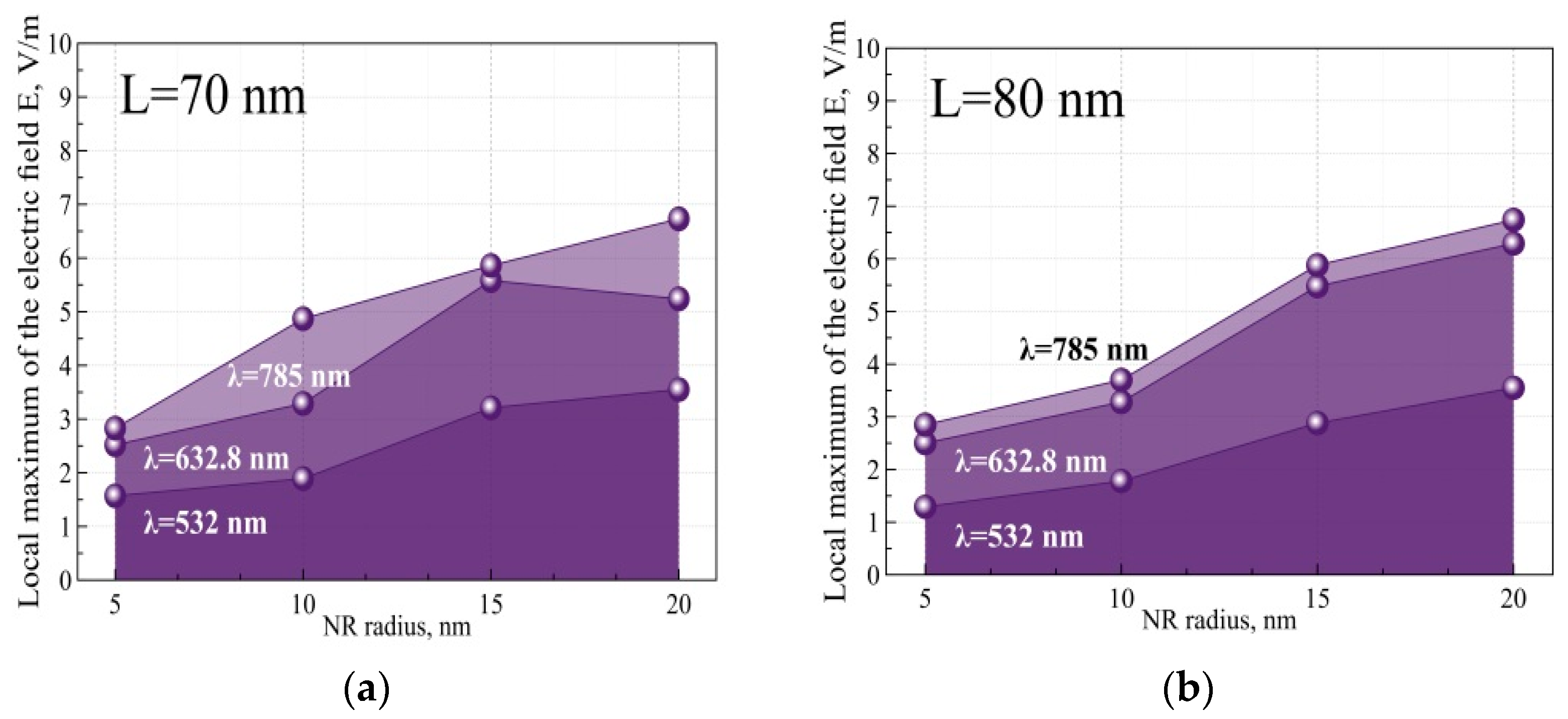
| 70 | 5 | 1.57 | 2.52 | 2.83 | 110 | 90 | 1040 | 1.22 | 0.8 | 110 |
| 10 | 1.89 | 3.29 | 4.87 | 140 | 133 | 2620 | 2 | 1.8 | 700 | |
| 15 | 3.21 | 5.58 | 5.86 | 462 | 500 | 3330 | 22 | 24 | 1100 | |
| 20 | 3.55 | 5.24 | 6.73 | 560 | 340 | 3770 | 29.5 | 12 | 1410 | |
| 80 | 5 | 1.29 | 2.5 | 2.85 | 109 | 105 | 1020 | 1.12 | 1.1 | 103 |
| 10 | 1.78 | 3.28 | 3.7 | 120 | 127 | 1300 | 1.43 | 1.6 | 165 | |
| 15 | 2.88 | 5.48 | 5.88 | 455 | 460 | 3150 | 21 | 21.4 | 1000 | |
| 20 | 3.55 | 6.29 | 6.74 | 520 | 530 | 3600 | 26.6 | 27.5 | 1320 | |
| NR Length, nm | NR Radius nm | Shell Thickness nm | 532 | 632.8 | 785 | 532 | 632.8 | 785 | 532 | 632.8 | 785 |
|---|---|---|---|---|---|---|---|---|---|---|---|
| Local Maximum of the Electric Field E, V/m | SERS Signal Intensity, a,u | Enhancement Coefficient | |||||||||
| 70 | 5 | 2 | 1.53 | 2.31 | 2.80 | 112 | 90 | 491 | 1.27 | 0.8 | 24.2 |
| 3 | 1.28 | 2.29 | 2.74 | 104 | 88 | 462 | 1.1 | 0.74 | 21.9 | ||
| 5 | 1.25 | 2.26 | 2.67 | 100 | 95 | 458 | 1 | 0.9 | 21.1 | ||
| 10 | 1.18 | 2.25 | 2.71 | 99 | 97 | 435 | 0.99 | 0.93 | 19.1 | ||
| 15 | 1.20 | 2.30 | 2.74 | 95 | 100 | 433 | 0.9 | 0.1 | 19 | ||
| 20 | 1.39 | 2.27 | 2.78 | 81 | 74 | 329 | 0.7 | 0.55 | 11 | ||
| 10 | 2 | 1.68 | 2.83 | 3.44 | 190 | 142 | 630 | 3.6 | 2.01 | 39 | |
| 3 | 16.3 | 2.68 | 3.16 | 162 | 130 | 1310 | 2.7 | 1.63 | 172 | ||
| 5 | 1.58 | 2.64 | 3.07 | 120 | 137 | 1350 | 1.41 | 1.85 | 182 | ||
| 10 | 1.39 | 2.58 | 2.97 | 150 | 116 | 1260 | 2.21 | 1.34 | 158 | ||
| 15 | 1.45 | 2.58 | 2.93 | 169 | 104 | 710 | 2.8 | 1.1 | 50 | ||
| 20 | 1.57 | 2.52 | 2.88 | 165 | 123 | 730 | 2.71 | 1.51 | 53 | ||
| 15 | 2 | 3.23 | 3.83 | 5.92 | 700 | 520 | 2410 | 48.5 | 27 | 600 | |
| 3 | 3.66 | 3.70 | 5.43 | 620 | 379 | 2290 | 39 | 14.4 | 520 | ||
| 5 | 3.72 | 4.38 | 5.06 | 710 | 610 | 3790 | 49.1 | 37.2 | 1490 | ||
| 10 | 3.91 | 4.62 | 5.17 | 1050 | 910 | 4800 | 110 | 83 | 2340 | ||
| 15 | 3.78 | 4.93 | 5.54 | 1100 | 1200 | 5400 | 120 | 145 | 2800 | ||
| 20 | 4.07 | 6.14 | 5.68 | 1320 | 1360 | 4400 | 173 | 185 | 1950 | ||
| 20 | 2 | 3.47 | 6.34 | 6.68 | 840 | 550 | 2430 | 70 | 29 | 600 | |
| 3 | 3.35 | 6.10 | 6.38 | 620 | 493 | 2600 | 38 | 24.4 | 700 | ||
| 5 | 3.64 | 5.96 | 5.68 | 900 | 905 | 3810 | 80 | 83 | 1500 | ||
| 10 | 3.84 | 6.48 | 5.79 | 1200 | 1100 | 4800 | 155 | 114 | 2400 | ||
| 15 | 3.91 | 6.92 | 6.28 | 1500 | 1500 | 5400 | 220 | 223 | 2800 | ||
| 20 | 3.97 | 7.34 | 6.55 | 1550 | 1700 | 6000 | 243 | 283 | 3150 | ||
| 80 | 5 | 2 | 1.45 | 2.49 | 2.70 | 110 | 100 | 990 | 1.14 | 1 | 930 |
| 3 | 1.39 | 2.35 | 2.66 | 102 | 95 | 910 | 10.4 | 0.9 | 850 | ||
| 5 | 1.39 | 2.32 | 2.58 | 100 | 91 | 920 | 9.6 | 8.4 | 860 | ||
| 10 | 1.32 | 2.29 | 2.58 | 99 | 92 | 910 | 9.5 | 0.89 | 850 | ||
| 15 | 1.27 | 2.22 | 2.62 | 99 | 109 | 910 | 9.5 | 11.2 | 850 | ||
| 20 | 1.31 | 2.19 | 2.63 | 80 | 80 | 700 | 0.6 | 6.6 | 435 | ||
| 10 | 2 | 1.51 | 2.84 | 3.45 | 190 | 161 | 600 | 3.5 | 2.6 | 35 | |
| 3 | 1.53 | 2.79 | 3.37 | 164 | 150 | 670 | 2.7 | 2.16 | 42.1 | ||
| 5 | 1.41 | 2.68 | 3.26 | 140 | 114 | 690 | 1.9 | 1.3 | 45.2 | ||
| 10 | 1.43 | 2.58 | 3.17 | 142 | 114 | 890 | 2 | 1.3 | 77 | ||
| 15 | 1.45 | 2.56 | 3.11 | 160 | 119 | 400 | 2.5 | 1.35 | 16.1 | ||
| 20 | 1.64 | 2.35 | 3.06 | 180 | 173 | 380 | 3.15 | 3 | 14.5 | ||
| 15 | 2 | 3.19 | 5.45 | 6.00 | 500 | 600 | 2520 | 25.2 | 33.2 | 650 | |
| 3 | 3.50 | 5.39 | 5.70 | 600 | 478 | 2500 | 35 | 23 | 620 | ||
| 5 | 3.68 | 5.16 | 5.12 | 570 | 421 | 3810 | 29 | 18.2 | 1470 | ||
| 10 | 3.89 | 5.50 | 5.10 | 700 | 432 | 4820 | 45 | 19 | 2350 | ||
| 15 | 3.94 | 6.01 | 5.56 | 840 | 530 | 5400 | 70 | 27.3 | 2840 | ||
| 20 | 4.02 | 5.87 | 5.71 | 990 | 530 | 3200 | 93 | 27.3 | 1040 | ||
| 20 | 2 | 3.20 | 6.35 | 6.58 | 600 | 640 | 2820 | 33.1 | 40.5 | 800 | |
| 3 | 3.37 | 6.05 | 6.30 | 680 | 600 | 2610 | 42.4 | 33.1 | 700 | ||
| 5 | 3.67 | 5.82 | 5.60 | 600 | 520 | 2100 | 34.2 | 27 | 422 | ||
| 10 | 3.89 | 6.13 | 5.74 | 660 | 580 | 2800 | 41.7 | 31 | 795 | ||
| 15 | 3.99 | 6.65 | 6.19 | 750 | 720 | 2820 | 60 | 52 | 805 | ||
| 20 | 4.02 | 7.07 | 6.40 | 990 | 890 | 3600 | 95 | 76 | 1300 | ||
| Shell Length, nm | Inner Shell Radius, nm | Shell Thickness, nm | 532 | 632.8 | 785 | 532 | 632.8 | 785 | 532 | 632.8 | 785 |
|---|---|---|---|---|---|---|---|---|---|---|---|
| Local Maximum of the Electric field E, V/m | SERS Signal Intensity, a,u | Enhancement Coefficient | |||||||||
| 70 | 5 | 2 | 1.11 | 1.91 | 2.20 | 63 | 56.5 | 121 | 0.395 | 0.32 | 1.45 |
| 3 | 1.16 | 1.94 | 2.26 | 70 | 62.1 | 130 | 0.43 | 0.38 | 1.7 | ||
| 5 | 1.16 | 1.99 | 2.24 | 72 | 57.6 | 145 | 0.5 | 0.33 | 2.1 | ||
| 10 | 1.10 | 2.06 | 2.57 | 80 | 78 | 385 | 0.63 | 0.58 | 15 | ||
| 15 | 1.32 | 2.12 | 2.65 | 90 | 94 | 420 | 0.77 | 0.89 | 18 | ||
| 20 | 1.29 | 2.04 | 2.78 | 51.4 | 71 | 268 | 0.27 | 0.45 | 6.9 | ||
| 10 | 2 | 1.02 | 1.85 | 2.43 | 61 | 74.6 | 286 | 0.36 | 0.56 | 8.3 | |
| 3 | 1.03 | 1.87 | 2.46 | 62.5 | 71 | 292 | 0.39 | 0.51 | 8.7 | ||
| 5 | 1.00 | 1.91 | 2.57 | 70 | 70 | 338 | 0.45 | 0.45 | 11.3 | ||
| 10 | 1.02 | 2.03 | 2.62 | 73 | 90 | 370 | 0.53 | 0.8 | 13.6 | ||
| 15 | 1.06 | 1.90 | 2.75 | 48.5 | 81 | 331 | 0.24 | 0.62 | 11 | ||
| 20 | 1.22 | 1.90 | 2.79 | 57.5 | 85 | 400 | 0.33 | 0.71 | 16 | ||
| 15 | 2 | 0.97 | 1.95 | 2.54 | 53.2 | 67.5 | 267 | 0.28 | 0.45 | 7.13 | |
| 3 | 0.94 | 1.85 | 2.61 | 60 | 78 | 312 | 0.36 | 0.59 | 9.9 | ||
| 5 | 1.01 | 1.92 | 2.61 | 60.6 | 86 | 380 | 0.37 | 0.74 | 14.5 | ||
| 10 | 1.18 | 1.99 | 2.62 | 56 | 58 | 130 | 0.31 | 0.34 | 1.65 | ||
| 15 | 1.23 | 2.05 | 2.71 | 62.8 | 59.9 | 140 | 0.40 | 0.37 | 1.9 | ||
| 20 | 1.18 | 2.14 | 2.77 | 61.6 | 70 | 164 | 0.38 | 0.44 | 2.69 | ||
| 20 | 2 | 1.04 | 1.91 | 2.64 | 44.4 | 61 | 236 | 0.2 | 0.37 | 5.55 | |
| 3 | 1.10 | 1.89 | 2.61 | 49.8 | 61 | 230 | 0.25 | 0.37 | 5.3 | ||
| 5 | 1.00 | 1.93 | 2.64 | 47 | 58.5 | 230 | 0.22 | 0.34 | 5.3 | ||
| 10 | 1.10 | 1.98 | 2.71 | 54.2 | 56.5 | 140 | 0.29 | 0.32 | 1.95 | ||
| 15 | 1.11 | 1.96 | 2.73 | 52.4 | 70 | 129 | 0.27 | 0.43 | 1.63 | ||
| 20 | 1.10 | 1.97 | 2.81 | 57.5 | 67 | 159 | 0.33 | 0.42 | 2.5 | ||
| 80 | 5 | 2 | 1.11 | 1.99 | 2.24 | 63 | 56 | 124 | 0.39 | 0.32 | 1.53 |
| 3 | 1.18 | 1.94 | 2.25 | 70 | 62 | 130 | 0.43 | 0.38 | 1.7 | ||
| 5 | 1.18 | 1.99 | 2.32 | 71 | 57.5 | 140 | 0.49 | 0.33 | 1.91 | ||
| 10 | 1.10 | 2.05 | 2.52 | 80 | 78 | 370 | 0.63 | 0.58 | 14 | ||
| 15 | 1.31 | 2.11 | 2.63 | 89 | 93 | 410 | 0.76 | 0.85 | 16.2 | ||
| 20 | 1.28 | 2.03 | 2.72 | 51.3 | 70 | 253 | 0.26 | 0.45 | 6.5 | ||
| 10 | 2 | 1.01 | 1.84 | 2.46 | 60 | 74.5 | 280 | 0.36 | 0.55 | 8 | |
| 3 | 0.99 | 1.86 | 2.45 | 61.5 | 71.1 | 291 | 0.38 | 0.52 | 8.5 | ||
| 5 | 1.00 | 1.88 | 2.50 | 62 | 61 | 330 | 0.38 | 0.45 | 11 | ||
| 10 | 1.02 | 2.02 | 2.59 | 73 | 90 | 365 | 0.53 | 0.8 | 13.5 | ||
| 15 | 1.05 | 1.89 | 2.69 | 48 | 80 | 333 | 0.24 | 0.6 | 11.3 | ||
| 20 | 1.21 | 1.89 | 2.73 | 57.5 | 85 | 415 | 0.33 | 0.71 | 16.5 | ||
| 15 | 2 | 0.96 | 1.94 | 2.59 | 52.4 | 67.5 | 270 | 0.27 | 0.45 | 7.2 | |
| 3 | 0.93 | 1.73 | 2.56 | 60 | 78 | 310 | 0.36 | 0.59 | 9.5 | ||
| 5 | 1.01 | 1.9 | 2.58 | 60.5 | 86 | 370 | 0.36 | 0.74 | 13.7 | ||
| 10 | 1.17 | 1.98 | 2.61 | 56.2 | 58 | 130 | 0.31 | 0.34 | 1.65 | ||
| 15 | 1.22 | 2.035 | 2.7 | 63 | 61 | 140 | 0.4 | 0.37 | 1.9 | ||
| 20 | 1.18 | 2.14 | 2.71 | 61 | 70 | 165 | 0.37 | 0.44 | 2.7 | ||
| 20 | 2 | 1.03 | 1.9 | 2.63 | 45 | 62 | 239 | 0.2 | 0.38 | 5.5 | |
| 3 | 1.08 | 1.875 | 2.62 | 50 | 61.5 | 232 | 0.25 | 0.37 | 5.35 | ||
| 5 | 0.99 | 1.92 | 2.64 | 47.1 | 59 | 233 | 0.22 | 0.34 | 5.36 | ||
| 10 | 1.07 | 1.975 | 2.7 | 53.5 | 57 | 140 | 0.29 | 0.32 | 1.95 | ||
| 15 | 1.01 | 1.96 | 2.73 | 52.5 | 70 | 130 | 0.28 | 0.43 | 1.65 | ||
| 20 | 1.09 | 2.04 | 2.8 | 58 | 66 | 160 | 0.34 | 0.42 | 2.52 | ||
| NR Length, nm | Inner Shell Radius, nm | Shell Thickness, nm | Au@SiO2 | Single (Hollow) SiO2 | ||||
|---|---|---|---|---|---|---|---|---|
| 532 | 632.8 | 785 | 532 | 632.8 | 785 | |||
| 5 | 2 | 15.0 | 23.0 | 19.1 | 12.8 | 26.8 | 32.3 | |
| 3 | 15.3 | 24.2 | 19.3 | 10.8 | 26.5 | 31.2 | ||
| 5 | 14.0 | 23.8 | 18.9 | 10.7 | 26.4 | 30.9 | ||
| 10 | 13.0 | 24.3 | 20.4 | 10.4 | 25.7 | 30.8 | ||
| 15 | 15.8 | 25.1 | 21.5 | 9.6 | 27.3 | 29.9 | ||
| 20 | 14.3 | 23.4 | 22.2 | 10.3 | 25.5 | 30.2 | ||
| 10 | 2 | 11.8 | 21.0 | 23.8 | 12.6 | 25.1 | 31.4 | |
| 3 | 11.1 | 21.4 | 23.9 | 12.1 | 24.1 | 29.5 | ||
| 5 | 12.9 | 21.5 | 25.6 | 11.8 | 23.3 | 29.6 | ||
| 10 | 11.7 | 22.7 | 27.0 | 11.6 | 22.4 | 28.2 | ||
| 15 | 8.5 | 21.9 | 27.6 | 12.2 | 21.5 | 26.9 | ||
| 20 | 10.2 | 21.8 | 28.0 | 12.3 | 22.0 | 26.5 | ||
| 15 | 2 | 9.4 | 22.6 | 23.4 | 16.0 | 28.0 | 39.9 | |
| 3 | 8.4 | 22.2 | 23.2 | 17.5 | 28.3 | 39.8 | ||
| 5 | 9.0 | 23.3 | 24.7 | 16.2 | 29.0 | 41.4 | ||
| 10 | 8.3 | 23.0 | 25.6 | 18.1 | 29.2 | 41.6 | ||
| 15 | 12.1 | 21.7 | 26.3 | 18.1 | 29.7 | 41.0 | ||
| 20 | 9.5 | 22.7 | 28.6 | 20.5 | 31.4 | 39.4 | ||
| 20 | 2 | 16.9 | 19.6 | 27.1 | 16.6 | 38.0 | 37.5 | |
| 3 | 17.1 | 19.5 | 27.0 | 18.4 | 33.3 | 38.3 | ||
| 5 | 17.3 | 19.4 | 26.4 | 18.3 | 36.1 | 38.2 | ||
| 10 | 17.4 | 19.9 | 27.2 | 19.8 | 36.9 | 37.4 | ||
| 15 | 17.7 | 21.3 | 27.4 | 19.6 | 37.7 | 37.4 | ||
| 20 | 17.9 | 21.6 | 28.4 | 20.2 | 39.6 | 38.7 | ||
| 80 | 5 | 2 | 20.6 | 21.2 | 21.2 | 14.2 | 28.1 | 19.2 |
| 3 | 20.0 | 22.4 | 21.2 | 13.9 | 29.1 | 18.3 | ||
| 4 | 19.2 | 22.1 | 21.1 | 13.2 | 28.9 | 17.7 | ||
| 10 | 20.2 | 22.5 | 22.8 | 12.7 | 28.0 | 16.3 | ||
| 15 | 20.8 | 23.2 | 24.0 | 11.3 | 28.1 | 17.1 | ||
| 20 | 19.4 | 22.5 | 25.0 | 10.6 | 26.6 | 17.4 | ||
| 10 | 2 | 20.2 | 19.4 | 28.0 | 15.6 | 28.6 | 21.7 | |
| 3 | 17.7 | 19.7 | 28.0 | 14.7 | 27.6 | 19.9 | ||
| 5 | 22.2 | 20.6 | 27.9 | 13.5 | 27.4 | 19.4 | ||
| 10 | 17.4 | 21.6 | 29.0 | 14.3 | 26.5 | 23.0 | ||
| 15 | 17.0 | 20.1 | 30.2 | 14.6 | 27.8 | 20.7 | ||
| 20 | 19.2 | 21.7 | 30.8 | 15.3 | 27.8 | 20.8 | ||
| 15 | 2 | 15.3 | 19.3 | 27.9 | 18.5 | 30.6 | 33.1 | |
| 3 | 15.0 | 20.0 | 27.8 | 20.3 | 31.2 | 33.0 | ||
| 5 | 15.9 | 20.0 | 29.4 | 22.1 | 32.0 | 33.2 | ||
| 10 | 18.7 | 21.1 | 27.9 | 21.2 | 33.4 | 31.9 | ||
| 15 | 18.5 | 21.6 | 29.0 | 22.2 | 33.4 | 34.1 | ||
| 20 | 17.3 | 22.7 | 28.7 | 22.9 | 32.6 | 34.8 | ||
| 20 | 2 | 15.8 | 19.5 | 31.4 | 19.6 | 33.4 | 37.5 | |
| 3 | 16.8 | 19.3 | 31.4 | 20.0 | 33.0 | 37.9 | ||
| 5 | 15.1 | 20.9 | 30.9 | 20.5 | 34.1 | 37.8 | ||
| 10 | 15.8 | 19.8 | 29.5 | 20.8 | 34.9 | 37.0 | ||
| 15 | 15.4 | 21.3 | 29.9 | 22.8 | 35.2 | 36.9 | ||
| 20 | 16.5 | 22.0 | 30.4 | 22.4 | 35.9 | 37.8 | ||
Publisher’s Note: MDPI stays neutral with regard to jurisdictional claims in published maps and institutional affiliations. |
© 2022 by the authors. Licensee MDPI, Basel, Switzerland. This article is an open access article distributed under the terms and conditions of the Creative Commons Attribution (CC BY) license (https://creativecommons.org/licenses/by/4.0/).
Share and Cite
Kon, I.; Zyubin, A.; Samusev, I. FDTD Simulations of Shell Scattering in Au@SiO2 Core–Shell Nanorods with SERS Activity for Sensory Purposes. Nanomaterials 2022, 12, 4011. https://doi.org/10.3390/nano12224011
Kon I, Zyubin A, Samusev I. FDTD Simulations of Shell Scattering in Au@SiO2 Core–Shell Nanorods with SERS Activity for Sensory Purposes. Nanomaterials. 2022; 12(22):4011. https://doi.org/10.3390/nano12224011
Chicago/Turabian StyleKon, Igor, Andrey Zyubin, and Ilia Samusev. 2022. "FDTD Simulations of Shell Scattering in Au@SiO2 Core–Shell Nanorods with SERS Activity for Sensory Purposes" Nanomaterials 12, no. 22: 4011. https://doi.org/10.3390/nano12224011
APA StyleKon, I., Zyubin, A., & Samusev, I. (2022). FDTD Simulations of Shell Scattering in Au@SiO2 Core–Shell Nanorods with SERS Activity for Sensory Purposes. Nanomaterials, 12(22), 4011. https://doi.org/10.3390/nano12224011