Article

Preparation of a ZnO Nanostructure as the Anode Material Using RF Magnetron Sputtering System

1
Department of Electrical Engineering, Hanbat National University, Daejeon 34158, Korea
2
Department of Electronic Engineering, Hanbat National University, Daejeon 34158, Korea
3
Department of Electrical & Computer Engineering, University of Florida, Gainesville, FL 32603, USA
*
Author to whom correspondence should be addressed.
Nanomaterials 2022, 12(2), 215; https://doi.org/10.3390/nano12020215
Submission received: 16 December 2021 / Revised: 5 January 2022 / Accepted: 6 January 2022 / Published: 10 January 2022
(This article belongs to the Special Issue Transparent Conductive Nanomaterials: Science and Applications)

Abstract

:
In this study, a four-inch zinc oxide (ZnO) nanostructure was synthesized using radio frequency (RF) magnetron sputtering to maximize the electrochemical performance of the anode material of a lithium-ion battery. All materials were grown on cleaned p-type silicon (100) wafers with a deposited copper layer inserted at the stage. The chamber of the RF magnetron sputtering system was injected with argon and oxygen gas for the growth of the ZnO films. A hydrogen (H2) reduction process was performed in a plasma enhanced chemical vapor deposition (PECVD) chamber to synthesize the ZnO nanostructure (ZnO NS) through modification of the surface structure of a ZnO film. Field emission scanning electron microscopy and atomic force microscopy were performed to confirm the surface and structural properties of the synthesized ZnO NS, and cyclic voltammetry was used to examine the electrochemical characteristics of the ZnO NS. Based on the Hall measurement, the ZnO NS subjected to H2 reduction had a higher electron mobility and lower resistivity than the ZnO film. The ZnO NS that was subjected to H2 reduction for 5 min and 10 min had average roughness of 3.117 nm and 3.418 nm, respectively.

1. Introduction

Many studies have recently been conducted on the viability of using transition metal oxides (Co, Ni, Cu, Mo, etc.) as anode materials for lithium-ion batteries. Transition metal oxides are attracting attention for such applications due to their specific capacity (which is two to three times higher than that of carbon) They are currently used as an anode material for conventional lithium-ion batteries [1,2,3,4,5,6,7,8,9,10,11,12,13,14,15]. Among the various transition metal oxides, zinc oxide (ZnO) is characterized by its low cost, easy manufacturing, chemical stability, large (60 mV) exciton binding energy, and 3.37 eV band gap [16,17]. When used as an anode material for lithium-ion batteries, ZnO has a high theoretical capacity of 978 mAhg−1 and a large lithium-ion diffusion coefficient [18,19,20,21]. However, given the low electrical conductivity of ZnO, as the charge/discharge cycle progresses, the large volume changes (228%) during the lithiation and delithiation processes reduce the stability of the specific capacity of ZnO [22,23].
The radio frequency (RF) magnetron sputtering system is an example of a physical vapor deposition method. When the RF power is supplied to the target, glow discharge occurs, which prompts the argon (Ar) atoms to conflict with the target. The target particles with smaller binding energy erupt due to the collision with Ar atoms. These erupted target particles adhere to the substrate and form a thin film [24,25].
In this paper, a ZnO film was deposited using an RF magnetron sputtering system, and ZnO nanostructures (ZnO NS) were prepared through hydrogen (H2) reduction. Among the various methods of compensating for the disadvantages of ZnO, one of the most effective methods is changing its structure. The reduction treatment was performed in an H2 gas atmosphere to widen the active area, and ZnO NS was used as the anode material.

2. Experiment Details

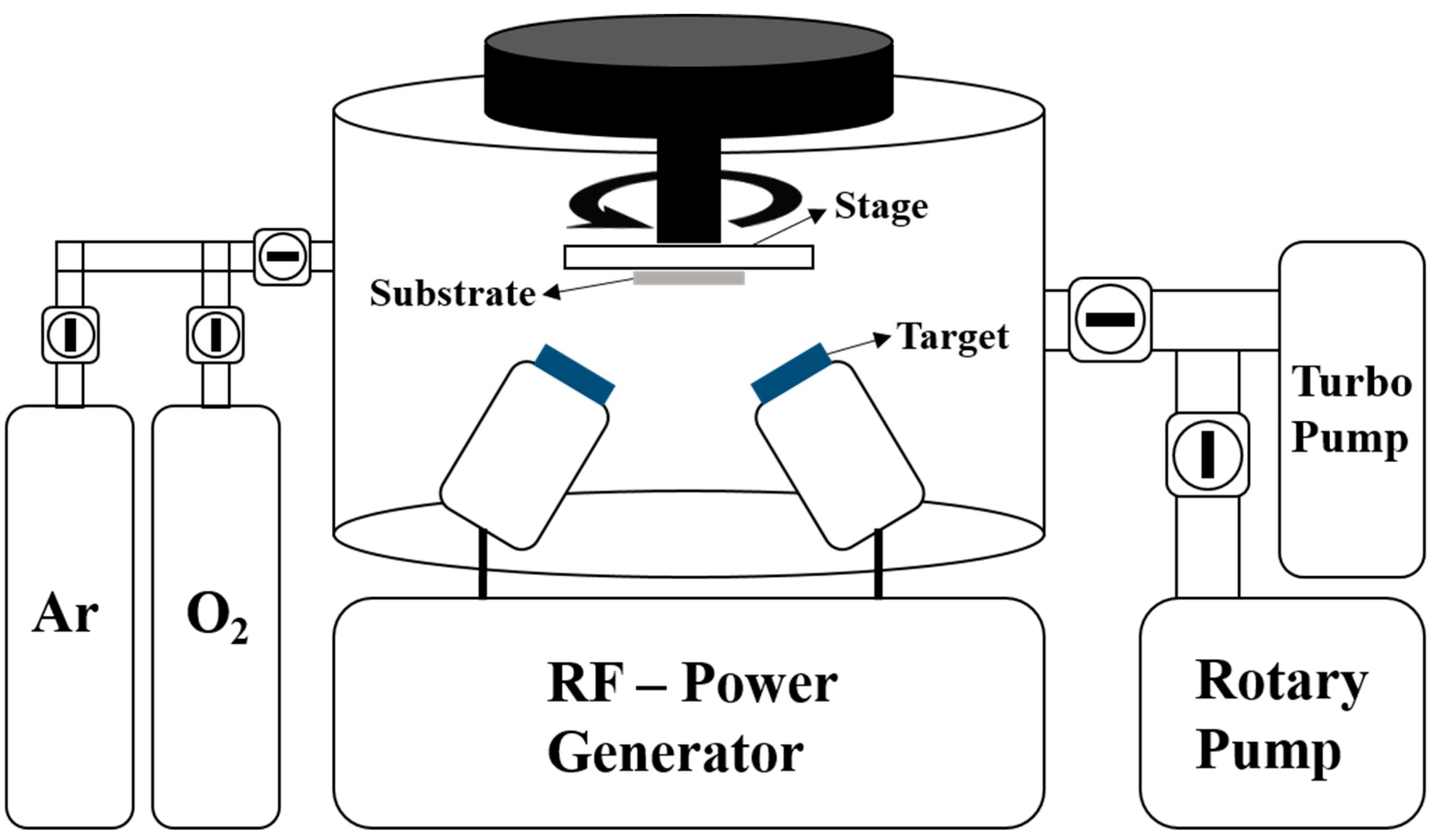
2.1. Preparation of Substrates and Copper (Cu) Layer Deposition

P-type silicon (Si, 100) was used to produce substrates. It was first cleaned to remove impurities. Then, the 2 × 2   cm Si substrates were added to a trichloroethylene (TCE) solvent and cleaned sequentially with ultrasonic cleaners (i.e., acetone, methanol, and deionized (DI) water) for 10 min each, after which they were dried using a nitrogen (N2) gas gun. The cleaned Si substrates were installed on the stage of the RF magnetron sputtering system and inserted into its chamber (I.T.S, Daejeon, Korea, PG600A-600W).
The base pressure of the sputtering chamber was 5 × 10 5   Torr , and the atmosphere of the chamber was composed of argon (Ar) gas. Pre-sputtering was performed for five minutes to remove impurities in the chamber. The Cu layer deposition process was carried out in the Ar atmosphere at a working pressure of 1.5 × 10 2   Torr using a four-inch Cu target. The detailed deposition conditions for the Cu layer are shown in Table 1, and the schematic diagram of the RF sputtering system is shown in Figure 1.

2.2. ZnO Film Deposition

For the deposition of the ZnO film, after the deposition of the Cu layer of the Si substrate, the Si substrate was inserted into the chamber of the RF magnetron sputtering system. The base pressure of the chamber was 5 × 10 5   Torr and the atmosphere of the chamber was made up of a mixture of Ar and oxygen (O2) gas at a ratio of 3:1. Pre-sputtering was performed for five minutes to remove impurities in the chamber, after which the ZnO film was deposited at 250 °C with 150   W RF plasma power using a four-inch ZnO target. The detailed conditions of the deposition of the ZnO film are shown in Table 2.

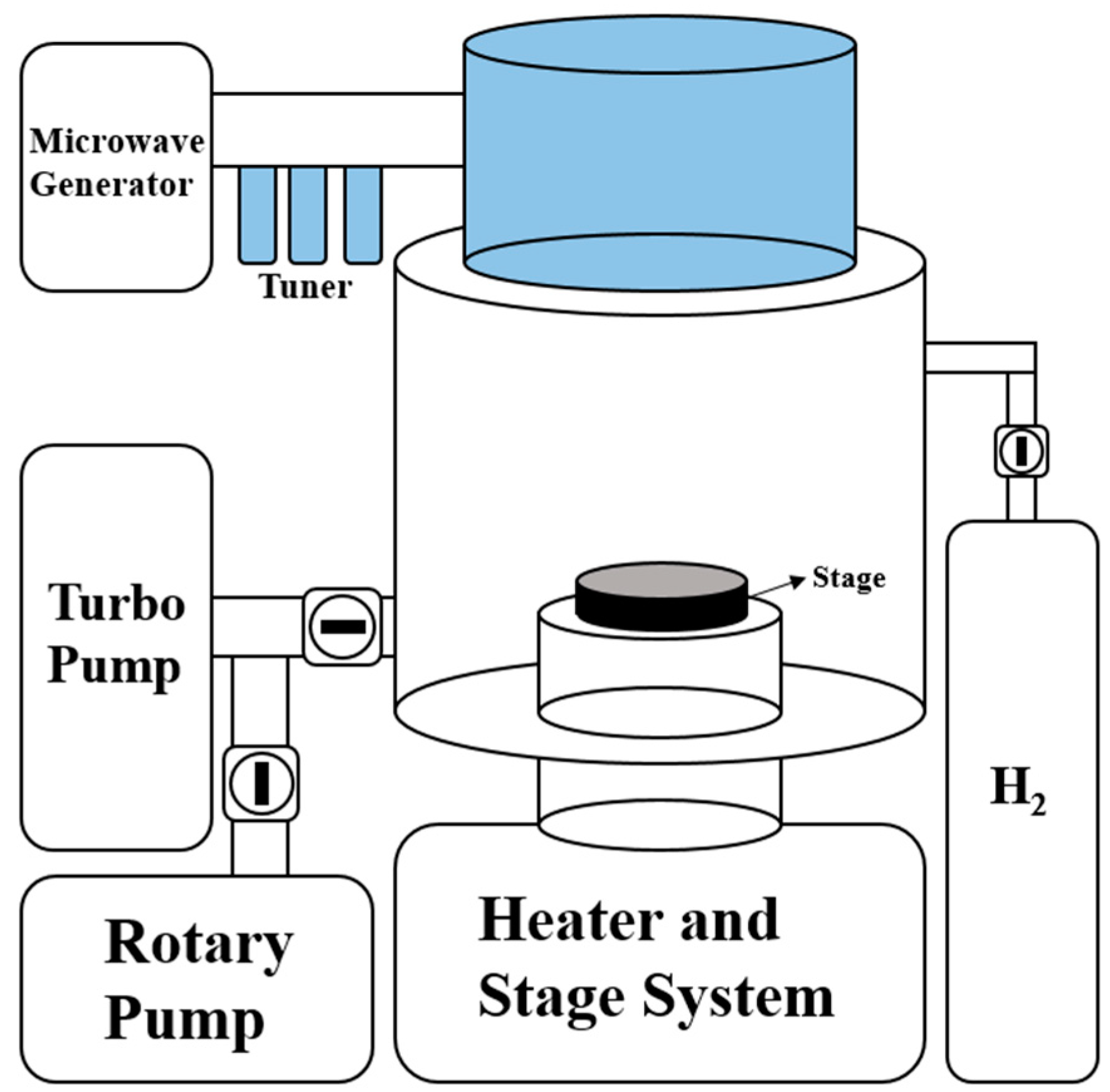
2.3. H2 Reduction Process

Plasma-enhanced chemical vapor deposition (PECVD, Woosin CryoVac, Uiwang, Korea, CVD-R2) was used for the H2 reduction of the ZnO film. The Cu-ZnO film previously prepared on the Si substrates was inserted into the stage of the PECVD chamber. The base pressure was set at 5 × 10 5   Torr , and the stage temperature at 600 °C. The ZnO NS was synthesized through H2 reduction of the ZnO film by injecting H2 into the PECVD chamber. The H2 injected into the chamber combined with the O2 in the ZnO film and caused a reduction reaction that escaped as water vapor. The H2 reduction process was performed for 5 min and 10 min for each sample. The PECVD schematic diagrams are shown in Figure 2, and the detailed H2 reduction processes are shown in Table 3.

2.4. Analysis

Field emission scanning electron microscopy (FE-SEM, Hitachi, Tokyo, Japan, S-4800), energy dispersive spectrometry (EDS, Oxford Instrument, Abingdon-on-Thames, United Kingdom, X-MAX), and atomic force microscopy (AFM, Park System, Suwon, Korea, XE-100) analysis were performed for the ZnO NS prepared on an Si wafer, and Hall measurement (ECOPIA, Anyang, Korea, HMS-3000) and cyclic voltammetry (CV, Autolab Instruments, Ionenstrasse, Switzerland, ECO CHEMIE PGSTAT 100) analysis were performed to determine the electrical conductivity and the oxidation-reduction characteristics. The CV test was performed the ZnO NS working electrode in 1M of sodium chloride (NaCl) electrolyte. The counter electrode was platinum (Pt) and the reference electrode was Ag/AgCl. The potential range of CV test was −0.8 V to 0 V, while the scan rate was 50 mV/s.

3. Results and Discussion

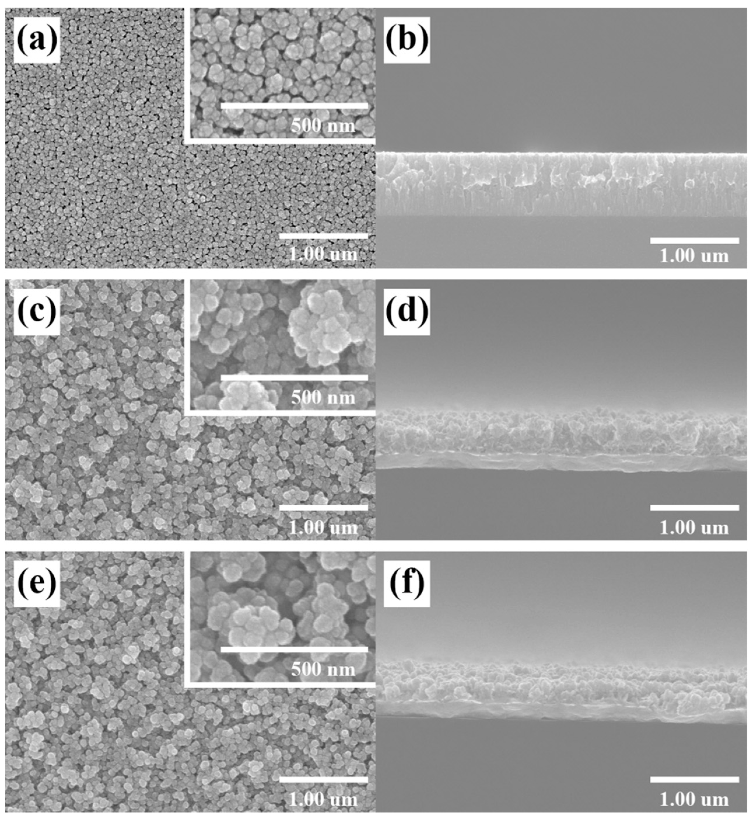
3.1. Field Emission Scanning Electron Microscopy (FESEM)

Figure 3 shows the surface and cross-section FESEM images of the ZnO NS. Figure 3a,b how the surface and cross-section, respectively, of the ZnO film deposited on the Cu layer before the H2 reduction process was performed. Figure 3c,d show the surface and cross-section, respectively, of the ZnO NS on which the H2 reduction process was performed for five minutes. During the H2 reduction process, the ZnO film was etched with H2 and its structure changed. Therefore, it can be confirmed that the surface area of H2 is wider than that of the ZnO film. In addition, Figure 3e,f show the surface and cross-section, respectively, of the ZnO nanostructure that was etched with H2 for 10 min.

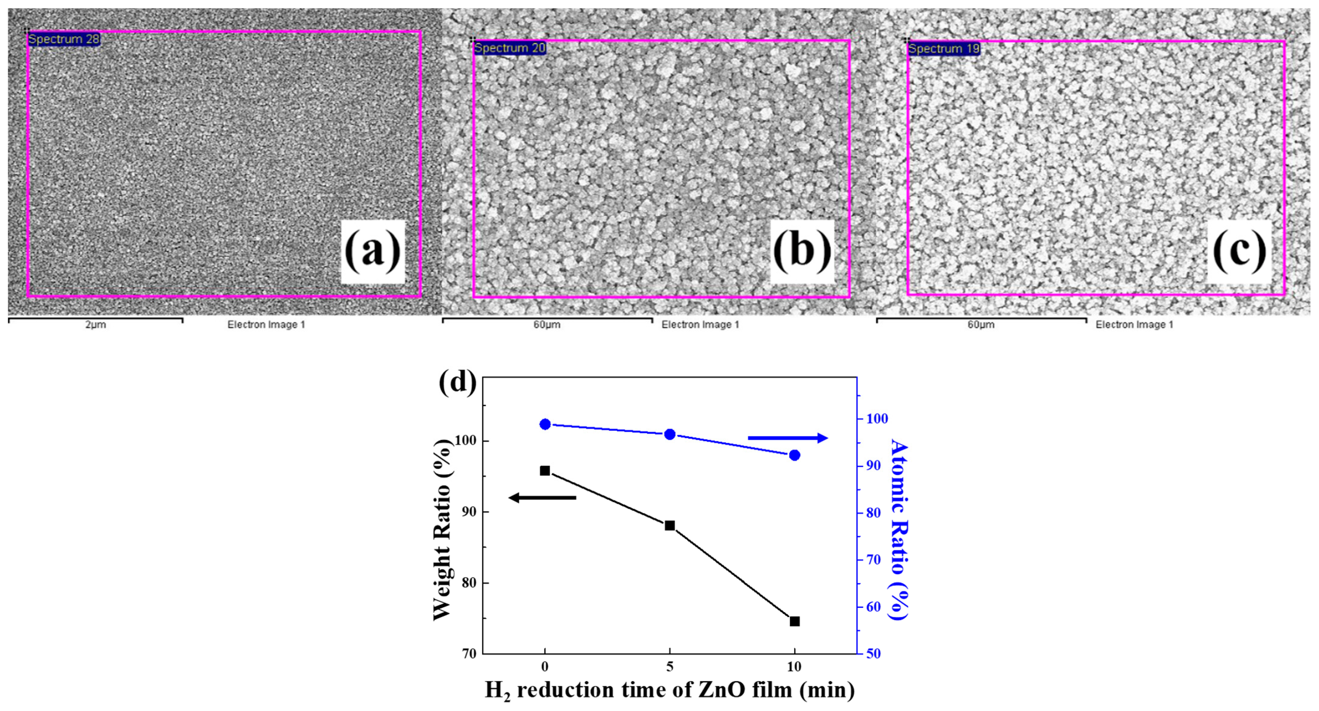
3.2. Energy Dispersive Spectrometry (EDS)

The ratios of zinc (Zn) and O2 in the ZnO film and the ZnO NS were confirmed through EDS analysis. The EDS measurement area of the ZnO film to which the H2 reduction process was not applied is shown in Figure 4a. Figure 4b,c show the EDS measurement area of the ZnO NS surface on which the H2 reduction process was performed for 5 and 10 min, respectively. The weight ratio and the atomic ratio of Zn and O2, which were determined using EDS analysis, are shown in Table 4. The weight ratio and the atomic ratio of the ZnO film and the ZnO NS that changed during the H2 reduction process are shown in Figure 4d. The figure shows that the longer the H2 reduction process, the lower the proportions of O2 in the ZnO film and in the ZnO NS. This was caused by the reaction of H2 and O2 during the H2 reduction process, which escaped as water vapor.

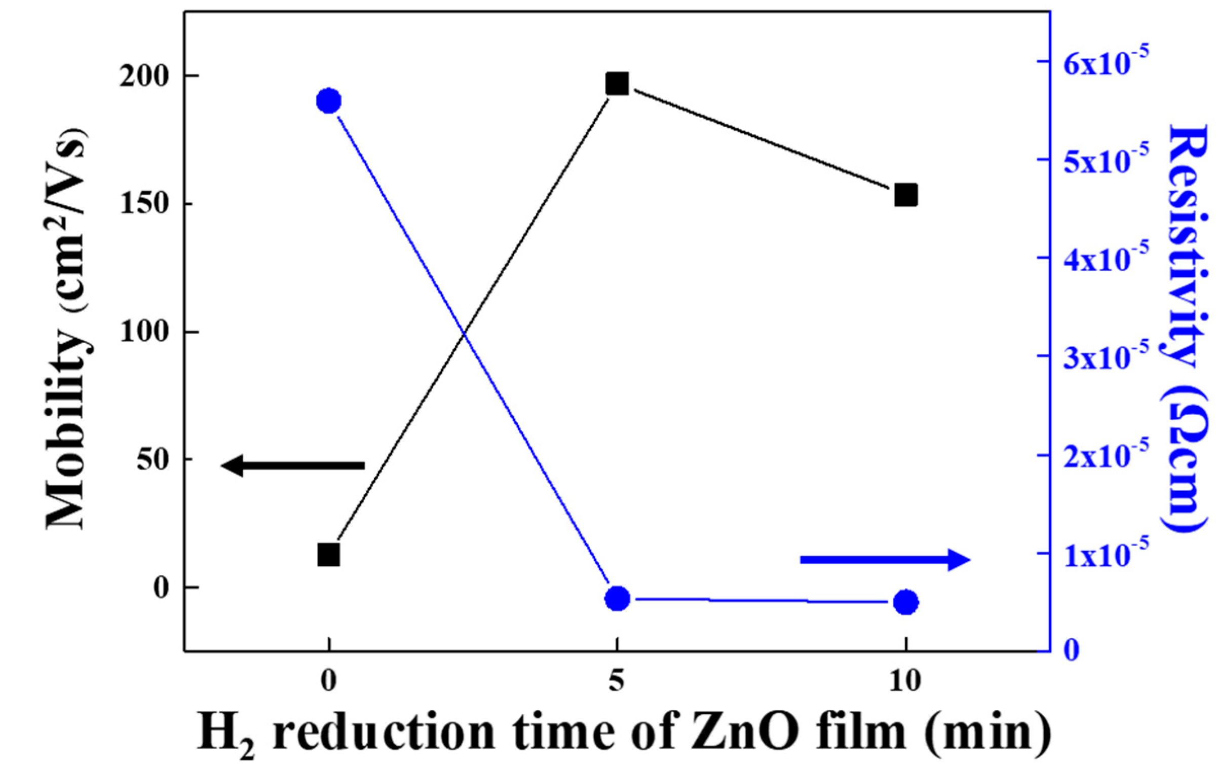
3.3. Hall Measurement

Hall measurement was performed on the ZnO films and on the ZnO NS. The graph in Figure 5 shows the mobility and resistance of the ZnO film and the ZnO NS. It shows that the ZnO NS subjected to H2 reduction had higher electron mobility and lower resistivity than the ZnO film. Although ZnO NS that was subjected to H2 reduction for five minutes showed higher electron mobility than the ZnO film subjected to H2 reduction for 10 min, their resistivity values were similar. These results show that the low electrical conductivity of the ZnO film can be increased through H2 reduction.

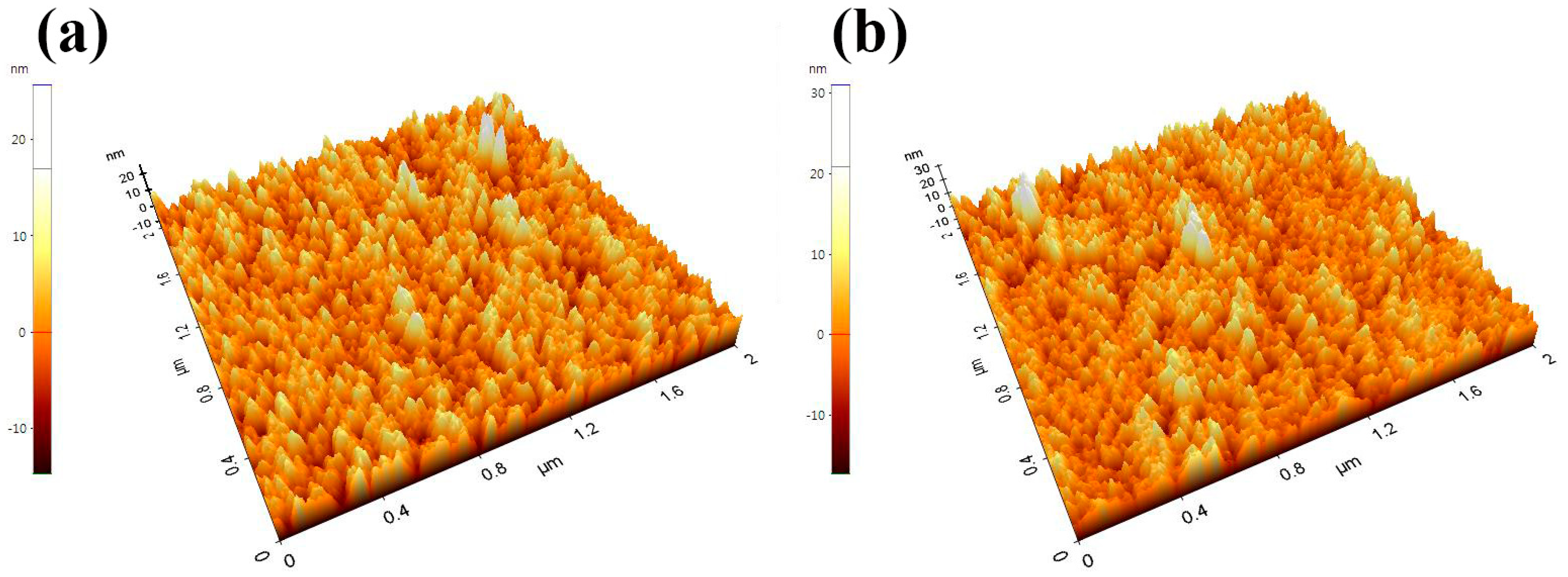
3.4. Atomic Force Microscopy (AFM)

The surface roughness was confirmed through AFM analysis of the ZnO NS. The average roughness (Ra) of the ZnO NS that was subjected to H2 reduction for five minutes was 3.117 nm, and its root mean square roughness (Rq) was 3.970 nm. The ZnO NS that was subjected to H2 reduction for 10 min had an Ra of 3.418 nm and an Rq of 4.427 nm. The comparison of the surface roughness values showed that the surface of the ZnO NS that was subjected to H2 reduction for 10 min was rougher. Figure 6a,b show the three-dimensional (3D) AFM images of the ZnO NS on which H2 reduction was performed for five minutes and 10 min, respectively, and Table 5 summarizes the main parameters of the AFM analysis for the ZnO NS.

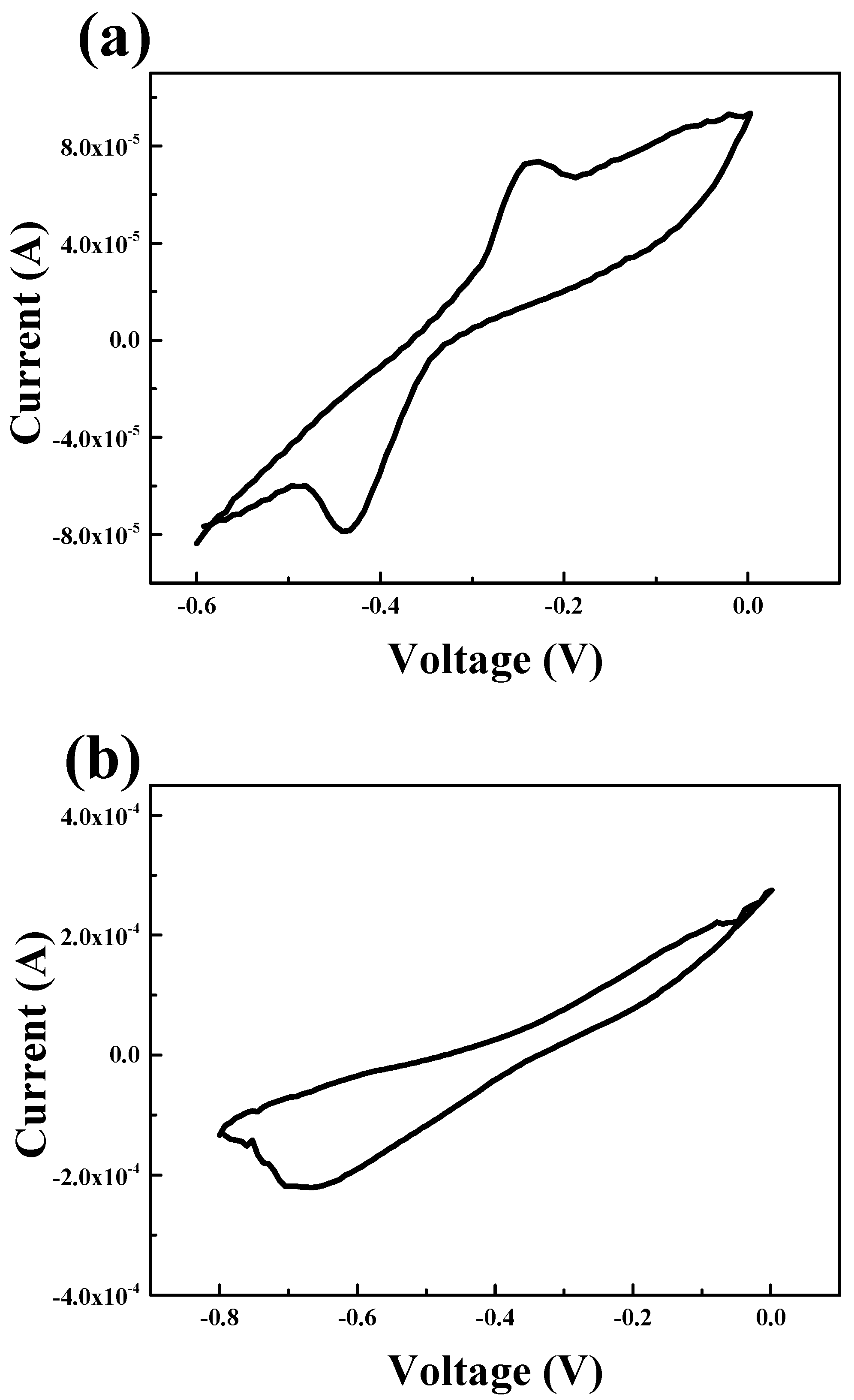
3.5. Cyclic Voltammetry (CV)

Figure 7 shows the CV curve of the ZnO NS. Figure 7a is the CV curve for the ZnO NS in which H2 reduction was performed for five minutes. One oxidation peak at −2.4 V and one reduction peak at −4.4 V were observed. On the other hand, on the CV curve of the ZnO NS on which H2 reduction was performed for 10 min, as shown in Figure 7b, one reduction peak was observed at −6.4 V but no oxidation peak was observed. On a CV curve, if only an oxidation peak or a reduction peak is observed, it indicates that an irreversible reaction is occurring rather than a reversible reaction. Accordingly, it can be confirmed that ZnO NS subjected to H2 reduction for 5 min exhibits a reversible reaction that can be utilized as an anode material for a lithium-ion battery. However, ZnO NS subjected to H2 reduction for 10 min is expected to be difficult to apply as an anode material for lithium-ion batteries.

4. Conclusions

In this study, a ZnO NS was prepared. When it was subjected to H2 reduction, its structure changed and it was confirmed to have had higher electrical conductivity than the ZnO film. In addition, its roughness value was measured and its CV curve was analyzed. The CV curve showed that its properties of oxidation-reduction reaction as the anode material improved when it was subjected to H2 reduction for five minutes. Therefore, the ZnO nanostructure can be applied as an anode material for lithium-ion batteries.

Author Contributions

Conceptualization, S.L. and W.C.; Data curation, S.L., Y.-H.J. and Y.-K.Y.; Formal analysis, S.L.; Investigation, S.L., Y.-H.J. and Y.-K.Y.; Writing-original draft, S.L.; Supervision, W.C All authors have read and agreed to the published version of the manuscript.

Funding

This work was supported by the Korea Institute of Energy Technology Evaluation and Planning (KETEP), the Ministry of Trade, Industry and Energy (MOTIE) of the Republic of Korea (No. 20204030200080) and the Korea Electric Power Corporation. (Grant number: R17XA05-01).

Institutional Review Board Statement

Not applicable.

Informed Consent Statement

Not applicable.

Data Availability Statement

The data presented in this study are available in article.

Conflicts of Interest

The authors declare no conflict of interest.

References

  1. Xiao, L.; Li, E.; Yi, J.; Meng, W.; Wang, S.; Deng, B.; Liu, J. Enhancing the performance of nanostructured ZnO as an anode material for lithium-ion batteries by polydopamine-derived carbon coating and confined crystallization. J. Alloys Compd. 2018, 764, 545. [Google Scholar] [CrossRef]
  2. Zhao, J.; Zhang, Y.; Wang, Y.; Li, H.; Peng, Y. The application of nanostructured transition metal sulfides as anodes for lithium ion batteries. J. Energy Chem. 2018, 27, 1536. [Google Scholar] [CrossRef] [Green Version]
  3. Su, H.; Jaffer, S.; Yu, H. Transition metal oxides for sodium-ion batteries. Energy Storage Mater. 2016, 5, 116. [Google Scholar] [CrossRef]
  4. Yan, Y.; Wang, B.; Yan, C.; Kang, D. Decorating ZnO nanoflakes on carbon cloth: Free-standing, highly stable lithium-ion battery anodes. Ceram. Int. 2019, 45, 15906. [Google Scholar] [CrossRef]
  5. Wei, J.S.; Zhu, Z.Y.; Zhao, X.; Song, T.B.; Huang, J.H.; Zhang, Y.X.; Chen, L.; Niu, X.Q.; Wang, Y.G.; Xiong, H.M. Self-assembled ZnO-carbon dots anode materials for high performance nickel-zinc alkaline batteries. Chem. Eng. J. 2021, 425, 130660. [Google Scholar] [CrossRef]
  6. Song, Y.; Chen, Y.; Wang, Z.; Zhao, W.; Qin, C.; Yu, H.; Wang, X.; Bakenov, Z.; Zhang, Y. Defective ZnOx@porous carbon nanofiber network inducing dendrite-free zinc plating as zinc metal anode for high-performance aqueous rechargeable Zn/Na4Mn9O18 battery based on hybrid electrolyte. J. Power Sources 2022, 518, 230761. [Google Scholar] [CrossRef]
  7. Bui, V.K.H.; Pham, T.N.; Hur, J.; Lee, Y.C. Review of ZnO Binary and Ternary Composite Anodes for Lithium-Ion Batteries. Nanomaterials 2021, 11, 2001. [Google Scholar] [CrossRef]
  8. Deckenbach, D.; Schmeider, J.J. A 3D hierarchically porous nanoscale ZnO anode for high-energy rechargeable zinc-air batteries. J. Power Sources 2021, 488, 229393. [Google Scholar] [CrossRef]
  9. Joshi, N.; Silva, L.; Shimizu, F.M.; Mastelaro, V.R.; M’Pekoo, J.C.; Lin, L.; Oliveira, O.N., Jr. UV-assisted chemiresistors made with gold modified ZnO nanorods to detect ozone gas at room temperature. Microchim. Acta 2019, 186, 418. [Google Scholar] [CrossRef]
  10. Yudha, C.S.; Hutama, A.P.; Rahmawati, M.; Widiyandari, H.; Nursukatmo, H.; Nilasary, H.; Oktaviano, H.S.; Purwanto, A. Synthesis and Characterization of ZnO from Thermal Decomposition of Precipitated Zinc Oxalate Dihydrate as an Anode Material of Li-Ion Batteries. Energies 2021, 14, 5980. [Google Scholar] [CrossRef]
  11. Shah, D.K.; KC, D.; Akhtar, M.S.; Kim, C.Y.; Yang, O.B. Vertically Arranged Zinc Oxid-e Nanorods as Antireflection Layer for Crystalline Silicon Solar Cell: A Simulation Study of Photovoltaic Properties. Appl. Sci. 2020, 10, 6062. [Google Scholar] [CrossRef]
  12. Zhang, F.; Wang, B.; Shen, Y. Blue Luminescent ZnO Nanoclusters Stabilized by Esterifiable Polyamidoamine Dendrimers and their UV-Shielding Applications. Asian J. Chem. 2014, 26. [Google Scholar] [CrossRef]
  13. Han, Z.; Li, Y.; Chen, F.; Tang, S.; Wang, P. Preparation of ZnO/Ag2O Nano-fibers by Coaxial Electrospinning and Study of Their Photocatalytic Properties. Chem. J. Chin. Univ.-Chin. 2020, 41, 308–316. [Google Scholar]
  14. Han, Z.Y.; Li, Y.J.; Lin, X.; Wang, Z.Y.; Li, Z.Q.; Wang, H. Preparation and photoelectrocatalytic performance of Fe2O3/ZnO composite electrode loading on conductive glass. Chem. Res. Chin. Univ. 2018, 39, 771–778. [Google Scholar]
  15. Chen, S.; Zhou, S.; Fu, J.; Tang, S.; Wu, X.; Zhao, P.; Zhang, Z. A near infrared fluorescence imprinted sensor based on zinc oxide nanorods for rapid determination of ketoprofen. Anal. Methods 2021, 13, 2836–2846. [Google Scholar] [CrossRef] [PubMed]
  16. Bhati, V.; Ranwa, S.; Fanetti, M.; Valant, M.; Kumar, M. Efficient hydrogen sensor based on Ni-doped ZnO nanostructures by RF sputtering. Sens. Actuators B Chem. 2018, 255, 588. [Google Scholar] [CrossRef]
  17. Joshi, K.; Rawat, M.; Gautam, S.; Singh Ramola, R.; Singh, F. Band gap widening and narrowing in Cu-doped ZnO thin films. J. Alloys Compd. 2018, 680, 252–258. [Google Scholar] [CrossRef]
  18. Yuan, J.; Zhang, X.; Chen, C.; Hao, Y.; Agrawal, R.; Wang, C.; Li, W.; Yu, H.; Yu, Y.; Zhu, X.; et al. Facile fabrication of three-dimensional porous ZnO thin films on Ni foams for lithium ion battery anodes. Mater. Lett. 2017, 190, 37. [Google Scholar] [CrossRef] [Green Version]
  19. Quartarone, E.; Dall’Asta, V.; Resmini, A.; Tealdi, C.; Tredici, I.G.; Tamburini, U.A.; Mustarelli, P. Graphite-coated ZnO nanosheets as high-capacity, highly stable, and binder-free anodes for lithium-ion batteries. J. Power Sources 2016, 320, 314. [Google Scholar] [CrossRef]
  20. Wang, D.; Guo, J.; Cui, C.; Ma, J.; Cao, A. Controllable synthesis of CNT@ZnO composites with enhanced electrochemical properties for lithium-ion battery. Mater. Res. Bull. 2018, 101, 305. [Google Scholar] [CrossRef]
  21. Li, Y.; Huang, Y.; Wang, X.; Liu, W.; Yu, K.; Liang, C. Simple synthesis of rice husk hollow carbon-coated flower ZnO for the anode in a high performance lithium-ion battery. J. Phys. Chem. Solids 2020, 145, 109540. [Google Scholar] [CrossRef]
  22. Huang, X.; Xia, X.; Yuan, Y.; Zhou, F. Porous ZnO nanosheets grown on copper substrates as anodes for lithium ion batteries. Port. Electrochim. Acta 2011, 56, 4960. [Google Scholar] [CrossRef]
  23. Zhang, Y.; Wei, Y.; Li, H.; Zhao, Y.; Yin, F.; Wang, X. Simple fabrication of free-standing ZnO/graphene/carbon nanotube composite anode for lithium-ion batteries. Mater. Lett. 2016, 184, 235. [Google Scholar] [CrossRef]
  24. Yun, Y.H. Characterization of Ga-doped ZnO thin films prepared by RF magnetron sputtering method. J. Korean Cryst. Growth Cryst. Technol. 2021, 31, 73–77. [Google Scholar]
  25. Westwood, W.D. Magnetrons. In Sputter Deposition; AVS: New York, NY, USA, 2003; pp. 43–74. [Google Scholar]
Figure 1. Schematic diagram of the RF magnetron sputtering system used in this study to synthesize Cu and ZnO.
Nanomaterials 12 00215 g001
Figure 2. Schematic diagram of the PECVD used in this study to synthesize the ZnO NS using the H2 reduction process.
Nanomaterials 12 00215 g002
Figure 3. FESEM image of the surface (a) and cross-section (b) of the ZnO film; FESEM image of the surface (c) and cross-section (d) of the ZnO NS on which the H2 reduction process was performed for five minutes; FESEM image of the surface (e) and cross-section (f) of the ZnO NS on which the H2 reduction process was performed for 10 min.
Nanomaterials 12 00215 g003
Figure 4. EDS analysis area of the ZnO film (a); EDS analysis area of the ZnO NS on which the H2 reduction process was carried out for five minutes (b) and 10 min (c); graph (d) of the ratios of Zn and O2 in the ZnO film and the ZnO NS.
Nanomaterials 12 00215 g004
Figure 5. Hall measurement analysis to confirm the electrical conductivity of the ZnO film and the ZnO NS.
Nanomaterials 12 00215 g005
Figure 6. 3D AFM analysis images of the ZnO NS on which the H2 reduction process was performed for five minutes (a) and 10 min (b).
Nanomaterials 12 00215 g006
Figure 7. CV 2 of the ZnO NS on which the H2 reduction process was performed for 5 min (a) and 10 min (b).
Nanomaterials 12 00215 g007
Table 1. Details of the Cu layer deposition conditions.
SubstrateTargetRF Power (W)Base Pressure (Torr)Working Pressure
(Torr)
Deposition Time (min)Temperature
°C
Si (100)Cu300 5 × 10 5 1.5 × 10 2 15250
Table 2. Details of the ZnO film deposition conditions.
SubstrateTargetRF Power (W)Base Pressure ( Torr ) Working Pressure ( Torr ) Deposition Time (min)Temperature °C
Si wafer/Cu layerZnO150 5 × 10 5 1.5 × 10 2 20250
Table 3. Details of the H2 reduction process conditions.
SamplesSubstrateH2 (sccm)Base Pressure ( Torr ) Temperature °CProcess Time (min)
Sample 1Si wafer/Cu layer/ZnO film100 5 × 10 5 6005
Sample 2Si wafer/Cu layer/ZnO film100 5 × 10 5 60010
Table 4. Weight ratio and atomic ratio of Zn and O2 for the ZnO NS.
SamplesZn Weight (%)O2 Weight (%)Zn Atomic (%)O2 Atomic (%)
Cu-ZnO film4.2495.761.0798.93
ZnO NS (5 min)11.9788.033.2296.78
ZnO NS (10 min)25.3774.637.6892.32
Table 5. Parameters of the AFM analysis of the ZnO NS.
SamplesRaRqSkewness (Rsk)Kurtosis (Rku)
ZnO NS (5 min)3.1173.970−0.3734
ZnO NS (10 min)3.4184.427−0.6124.721
Publisher’s Note: MDPI stays neutral with regard to jurisdictional claims in published maps and institutional affiliations.

