Article

Enhanced Photodetection Range from Visible to Shortwave Infrared Light by ReSe2/MoTe2 van der Waals Heterostructure

1
School of Computer Science and Engineering, Macau University of Science and Technology, Avenida Wai Long, Taipa, Macao 999078, China
2
Institute of Microscale Optoelectronics, Collaborative Innovation Centre for Optoelectronic Science & Technology, Key Laboratory of Optoelectronic Devices and Systems of Ministry of Education and Guangdong Province, College of Physics and Optoelectronic Engineering, Shenzhen Key Laboratory of Micro-Nano Photonic Information Technology, Guangdong Laboratory of Artificial Intelligence and Digital Economy (SZ), Shenzhen University, Shenzhen 518060, China
3
Guangdong-HongKong-Macao Joint Laboratory for Intelligent Micro-Nano Optoelectronic Technology, Foshan University, Foshan 528225, China
*
Author to whom correspondence should be addressed.
These authors contributed equally to this work.
Nanomaterials 2022, 12(15), 2664; https://doi.org/10.3390/nano12152664
Submission received: 5 June 2022 / Revised: 31 July 2022 / Accepted: 1 August 2022 / Published: 3 August 2022
(This article belongs to the Special Issue Molecular Beam Epitaxy Growth of Quantum Wires and Quantum Dots)

Abstract

:
Type II vertical heterojunction is a good solution for long-wavelength light detection. Here, we report a rhenium selenide/molybdenum telluride (n-ReSe2/p-MoTe2) photodetector for high-performance photodetection in the broadband spectral range of 405–2000 nm. Due to the low Schottky barrier contact of the ReSe2/MoTe2 heterojunction, the rectification ratio (RR) of ~102 at ±5 V is realized. Besides, the photodetector can obtain maximum responsivity (R = 1.05 A/W) and specific detectivity (D* = 6.66 × 10¹¹ Jones) under the illumination of 655 nm incident light. When the incident wavelength is 1550–2000 nm, a photocurrent is generated due to the interlayer transition of carriers. This compact system can provide an opportunity to realize broadband infrared photodetection.

1. Introduction

Two-dimensional (2D) materials have gradually become one of the hotspots of current research since the emergence of graphene. Two-dimensional materials have been widely used in photodetectors [1,2], sensors [3,4], solar cells [5,6] and other fields because of their excellent optical, electronic and mechanical properties [7,8]. Transition metal dichalcogenides (TMDs) in particular, as a class of 2D materials, have attracted extensive attention from researchers [9]. TMDs have adjustable band gap from single layer to bulk, and they can convert direct band gap into indirect band gap by adding the number of layers [10], which enables TMD photodetectors to detect light from visible to near-infrared [11]. Moreover, TMDs have higher environmental stability than black phosphorus, which makes them applicable for devices intended to work in harsh conditions for a long time.
As a kind of typical 2D TMD, rhenium selenide (ReSe2) possesses a stable distorted 1T phase, which leads to its in-plane anisotropy [12,13,14]. ReSe2 exists as a layer-dependent band structure in the range of 1.3–1.1 eV from monolayer to bulk [15,16,17], which makes it an ideal candidate for constructing high-performance photodetectors in a broad spectrum [18]. Besides, the strong in-plane anisotropic properties of ReSe2 have also attracted extensive attention for developing high-performance polarized photodetectors [19].
However, the intrinsic bandgap in ReSe2 limits the detection wavelength to near-infrared range [19]. In order to overcome this limitation, heterojunctions based on four different schemes have been proposed [20]. The first scheme uses two materials to form a photoconductive structure, one for absorbing long wavelengths of light and another as a carrier transport channel [21]. The second scheme uses two kinds of materials to form a type II vertical heterojunction structure and uses the characteristics of type II heterojunction to accomplish the carrier interlayer transition [22]. The third scheme is to build a p-g-n structure [23], which uses graphene as a light-absorbing material in the middle layer. Due to the existence of a built-in electric field in the structure, the photogenerated carriers in graphene are effectively separated. The last one is to make a metal array on the surface of a 2D material [24]. It uses the surface plasmon resonance between the incident light and the metal to trap incident light.
Nowadays, ReSe2 has been widely used in photodetectors. Yang et al. constructed the layer-dependent ReSe2 photodetector by mechanical exfoliation method, and obtained a photoresponsivity of 95 A/W [17]. The ReSe2 doped by Co ions has been discussed by Khan et al., which not only improved the photocurrent of the photodetector, but also broadened the photodetection range [25]. However, the photoresponse speeds of these two photodetectors are relatively slow. Many photodetectors based on the structure of vertical heterojunctions can solve this problem [26]. The InSe/ReSe2 heterojunction photodetector was studied by Du et al. and the response speed was 0.36/0.39 ms [27]. However, the photodetection range of ReSe2-based vertical heterojunction photodetectors is mostly concentrated in the visible (VIS) to near-infrared band [28]. According to reports, the longest detection wavelength of ReSe2-based vertical heterojunction photodetectors is only 1550 nm [29].
In this work, we designed an n-ReSe2/p-MoTe2 vertical heterojunction photodetector for broadband photodetection. Benefiting from the characteristics of type II band alignment, this heterostructure can broaden the photodetection range of our photodetector, which covers visible to shortwave infrared (SWIR) bands. The key parameters of the photodetector were obtained, such as response time, responsivity (R) and specific detectivity (D*). Finally, the energy band alignments of the heterojunction photodetector were analyzed, and the mechanism of carrier interlayer transition was analyzed.

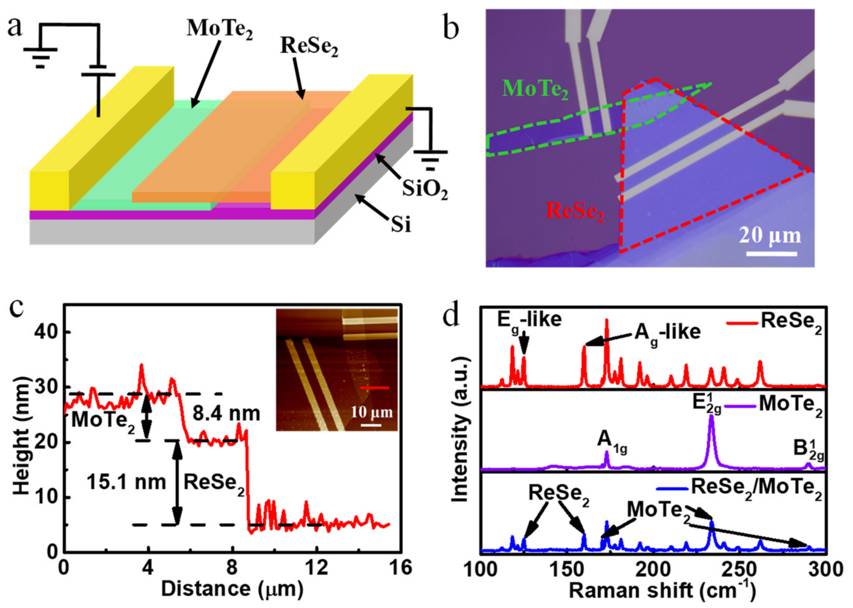
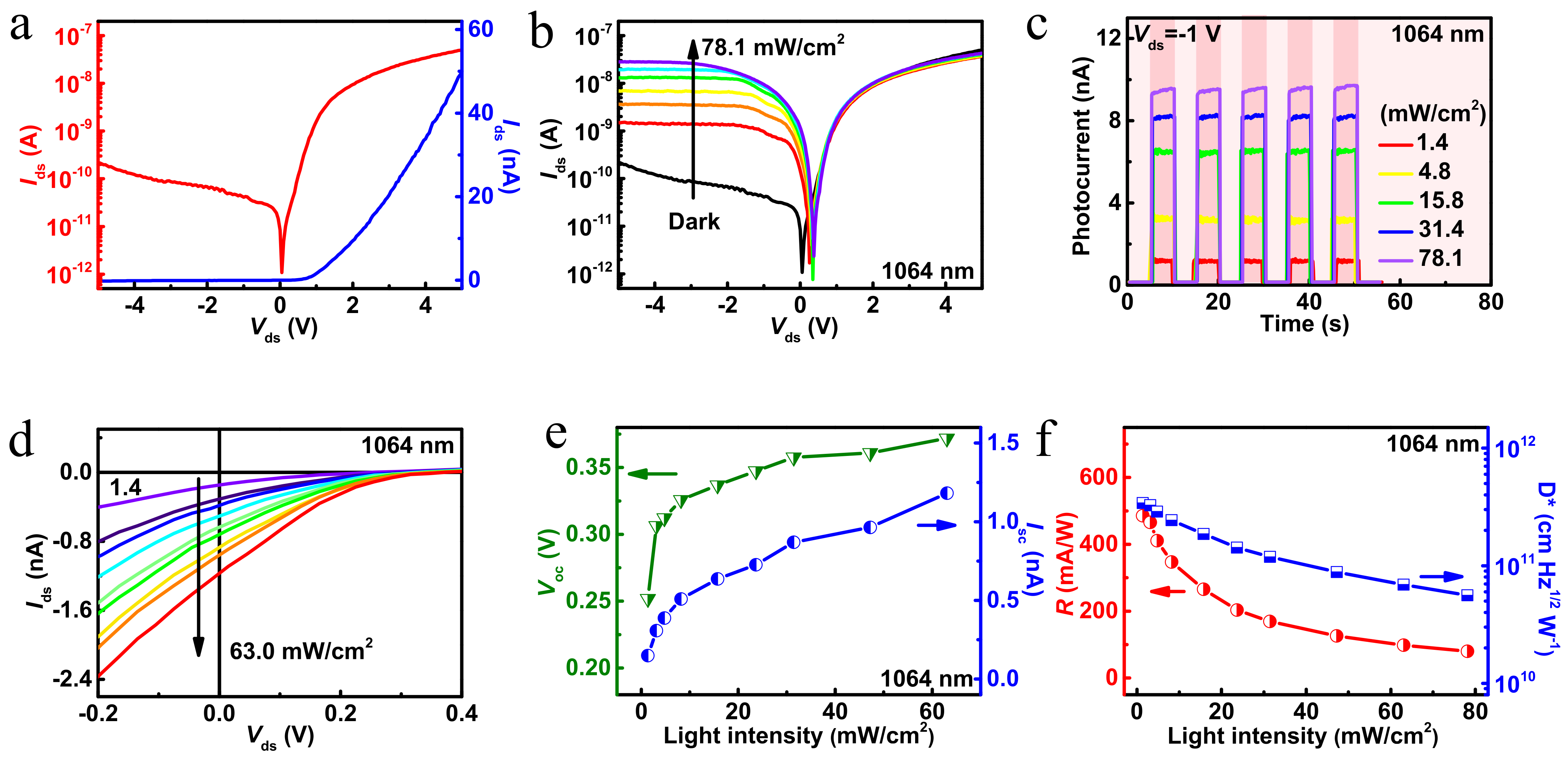
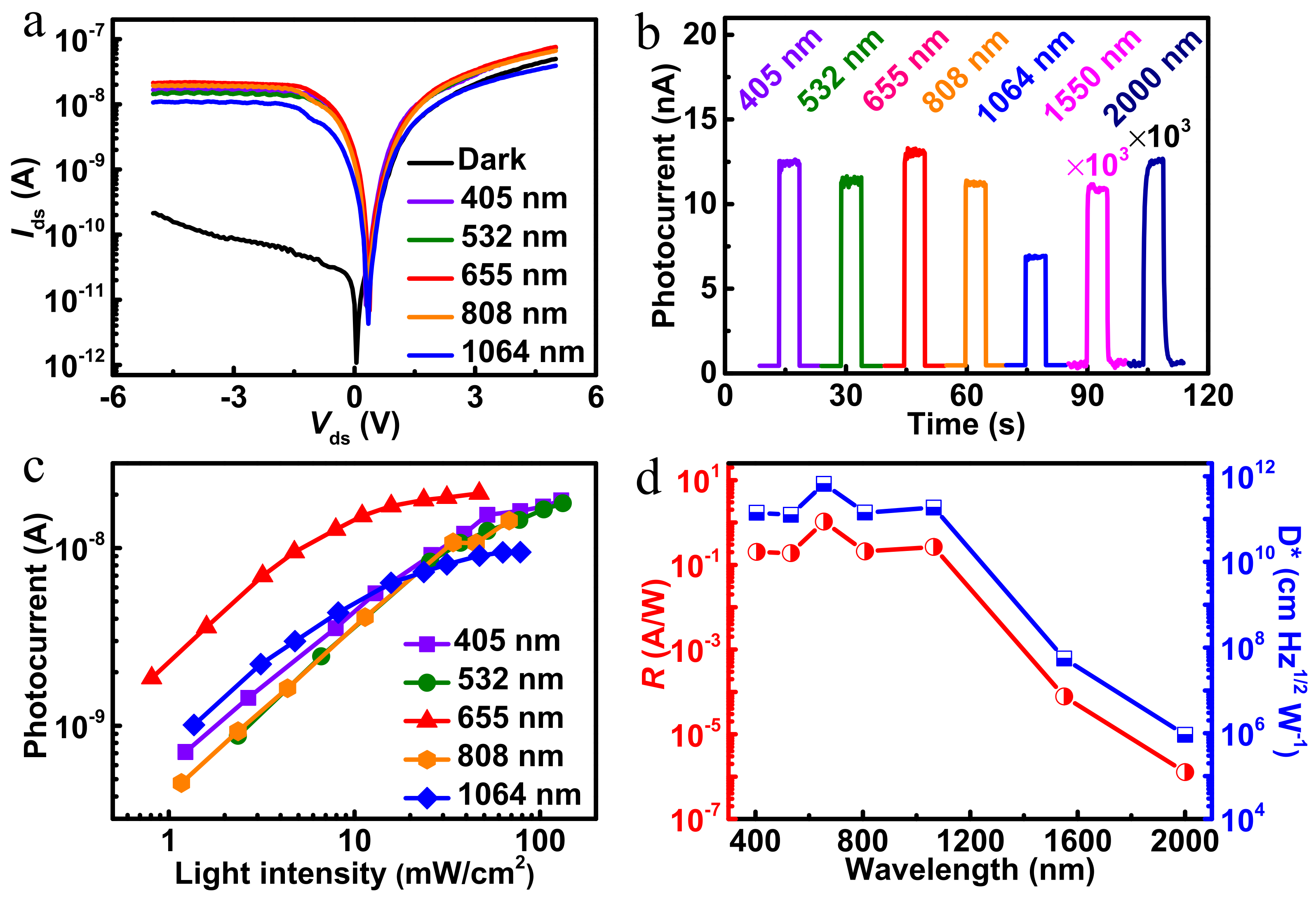
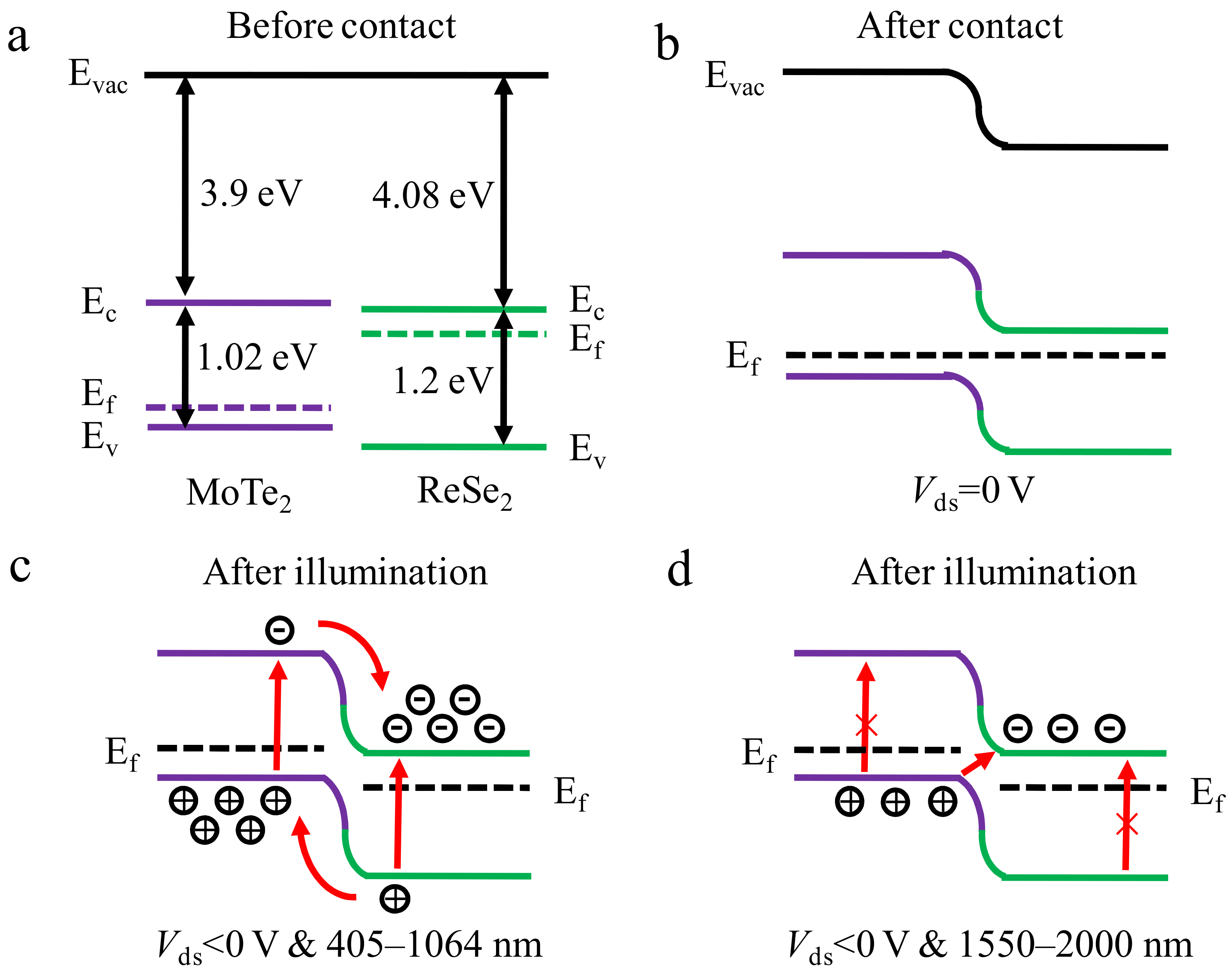
2. Results and Discussion

Figure 1a shows a configuration diagram of the ReSe2/MoTe2 Van der Waals heterostructure. Firstly, the ReSe2 and MoTe2 nanosheets were stacked on a 275 nm SiO2/Si substrate, and then the metal electrodes (Au 60 nm/Cr 10 nm) were deposited onto the two materials by electron beam lithography and electron beam evaporation (shown in experimental details). The optical image of the ReSe2/MoTe2 heterojunction is shown in Figure 1b. The ReSe2 flake is stacked on the MoTe2 flake, and metal electrodes are attached to the surfaces of both materials. The thicknesses of ReSe2 and MoTe2 nanosheets are 15.1 nm and 8.4 nm, respectively (Figure 1c). Additionally, the atomic force microscope (AFM) image of the device is shown in the inset. Besides, the red line in the inset represents the area where the thickness of the heterostructure is obtained. Raman scattering measurements were performed on the heterojunction photodetector using 532 nm laser excitation (Figure 1d). The peaks of 125.1 cm−1 and 159.9 cm−1 correspond to the Eg-like and Ag-like vibration mode of ReSe2, respectively [30]. Besides, the Raman characteristic peaks of MoTe2 are 173.2 cm−1, 233.6 cm−1 and 289.8 cm−1, which correspond to A1g, E 2 g 1 and B 2 g 1 vibration modes, respectively [31]. Raman characteristic peaks of ReSe2 and MoTe2 can be observed simultaneously in the heterojunction region. This means that the heterojunction region can reflect the characteristics of the two materials at the same time.
Next, the measurements of photoelectric properties were completed under ambient conditions at room temperature. In the experiment, the drain electrode and the source electrode were contacted to MoTe2 and ReSe2, respectively. Figure 2a depicts the current-voltage (I–V) characteristics of ReSe2/MoTe2 in a dark environment. According to the I–V curve, typical rectification characteristics are observed and the rectification ratio is about 102 at ±5 V. It indicates that a heterojunction is formed between ReSe2 and MoTe2, because the Au/Cr electrode provides good ohmic contact with ReSe2 and MoTe2, respectively (shown in Supplementary Figure S1). Furthermore, the source-drain current (Ids) in both ReSe2 and MoTe2 materials show positive photocurrent response characteristics under illumination. It is noteworthy that good contact resistance and ohmic characteristics are helpful to improve the performance of the device. The transmission characteristic curve (shown in Supplementary Figure S2) shows that the current increases with the raising of the positive gate voltage for ReSe2, showing an n-type behavior. Whereas the current increases with the raising of the negative gate voltage for MoTe2, indicating a p-type behavior. The rectification effect is related to the built-in electric field formed at the p-n junction between ReSe2 and MoTe2. Under positive bias, the built-in electric field formed at the p-n junction is greatly reduced, which means that electrons are easily transferred across layers leading to a significant conduction current. In contrast, under negative bias, the current is turned off because of the enhanced built-in potential. The quantification of photoresponse to various light intensities is an important experiment to determine the photodetection performance of the heterojunction. Therefore, we measured the characteristics of I-V logarithmic images of the photodetector under different light intensities of 1064 nm laser from dark to 78.1 mW/cm2 (Figure 2b). Obviously, under the negative bias, the photocurrent grows with the increase of light intensity, resulting in the reduction of rectification ratio. In addition, the time-dependent photocurrent of the photodetector at −1 V bias was studied under different light intensities of 1.4, 4.8, 15.8, 31.4 and 78.1 mW/cm2, which is shown in Figure 2c. As the light intensity was adjusted from 1.4 to 78.1 mW/cm2, the photocurrent increased from 1.16 to 9.59 nA. The reason for the high sensitivity under negative bias is that the increase of photoexcited carriers leads to the monotonic increase in photocurrent at higher light intensity. Time-dependent photoresponse of the ReSe2/MoTe2 heterojunction under varied light intensities (1064 nm, Vds = 1 V) has been added in Figure S3a shown in Supplementary Materials. Under positive bias, the photocurrent under different light intensities is relatively low and the noise is large. Besides, the photocurrent comparison curves of the photodetector under positive and negative bias are given in Figure S3b shown in Supplementary Materials. Next, the photovoltaic characteristics of the photodetector based on the ReSe2/MoTe2 heterostructure were further investigated in the light intensity range from 1.4 to 63.0 mW/cm2, which is shown in Figure 2d. It is worth noting that the photodetector possesses photovoltaic characteristics under light illumination without external bias. The extracted open-circuit voltage (Voc, left axis) and short-circuit current (Isc, right axis) show a growth trend (Figure 2e). The maximum values of Voc and Isc are 0.37 V and 1.18 nA, respectively. At the same time, the corresponding R and D* values under different power densities are calculated and plotted in Figure 2f. These two main parameters are calculated according to the following formula: R = ( I p I d ) / P opt , D * = R / 2 eJ d , where Ip, Id, Popt, e and Jd are the photocurrent, dark current, incident light power, electron charge (1.6 × 10⁻¹⁹ C) and effective dark current density (Jd = 6.3 × 10⁻⁶ A/cm2). The maximum values of R and D* are 485.6 mA/W and 3.4 × 10¹¹ Jones (Jones = cm Hz1/2 W−1), respectively, under the incident light with the power density of 1.4 mW/cm2 at −1 V bias. Meanwhile, it can be clearly found that R and D* decrease gradually with the increase of the power density, which is related to the trapping and recombination of the photo-carriers within the heterojunction [32,33,34].
The current of the photodetector under negative bias increases obviously (Figure 3a) with the illumination of different wavelengths (405, 532, 655, 808 and 1064 nm). The corresponding linear scale figure has been given in Supplementary Figure S4. Voc and Isc under different wavelengths of incident light are extracted and given in the support information (shown in Supplementary Figure S5). Subsequently, the real-time photoresponse characteristics of the device under laser light of various wavelengths at −1 V are represented in Figure 3b. Since the photoresponse of the device under 1550 nm and 2000 nm incident light is not of the same order of magnitude, the values of the photocurrent in the figure are multiplied by 1000. The phenomenon shown in the figure is not that there will be higher photocurrent under the irradiation of short wavelength incident light. This mainly depends on which wavelength the heterojunction material is sensitive to. Moreover, stable, fast and repeatable photoresponse curves under the laser light of different wavelengths are also given in the supporting information (shown in Supplementary Figure S6). The results show that the assembled heterojunction exhibits broadband photosensitivity in the range of ultraviolet (405 nm) to shortwave infrared (2000 nm). In order to further investigate the performance of the ReSe2/MoTe2 heterostructure photodetector, Figure 3c and Figure S7 (shown in supporting information) illustrate the optical power density dependence of photocurrent at different wavelengths (VIS-SWIR). Under 405–1064 nm light illumination, the photocurrent at Vds = −1 V increases monotonously with the raise of laser power at the low optical power density, and reaches saturation at high power density. The non-uniformity of photocurrent dependent on optical power density may be related to the increase of recombination activity of photogenerated charge carriers at high power density and the occurrence of trap states between the Fermi level and conduction band [35]. Under 1550 nm and 2000 nm illumination, the increase of photocurrent does not saturate with the increase of power density. In addition, the wavelength correlation R and D* of the ReSe2/MoTe2 heterostructure photodetector were also investigated, as shown in Figure 3d. Obviously, the device shows broadband photoresponse in the range of 405–2000 nm, and the peak response of R and D* reaches 1.05 A/W and 6.66 × 10¹¹ Jones at 655 nm, respectively. Our heterojunction device can detect visible to shortwave infrared light, even though its response drops dramatically in the 1550–2000 nm region. The R and D* of each wavelength at different power are given in the supporting information (shown in Supplementary Figure S8). The responsivity decreases with the increase of incident light intensity. When the incident light intensity increases, more photogenerated carriers will be generated. However, the increase of photogenerated carriers may increase the probability of carriers being trapped by defects, as well as carrier recombination and carrier scattering in the heterojunction, resulting in more carriers being wasted. According to the formula of responsivity, it follows that the more photoelectrons are wasted, the less the photocurrent can be generated, which ultimately leads to the decrease of responsivity.
Figure 4a shows the band alignment of ReSe2 and MoTe2 before contact. The electron affinities of ReSe2 and MoTe2 are 4.08 and 3.9 eV, respectively. The band gaps of ReSe2 and MoTe2 nanosheets are 1.2 and 1.02 eV, respectively [36,37]. According to Figure S2, the electrical characteristics of single ReSe2 and MoTe2 field-effect transistors (FET) are characterized to determine the carrier type. The ReSe2 device exhibits n-type characteristics, while the MoTe2 device exhibits p-type characteristics. This means that the Fermi level (Ef) of ReSe2 is close to the conduction band (Ec), while the Fermi level of MoTe2 is close to the valence band (Ev). After contact, the p-n heterojunction will be constructed, and the transmission of carriers leads to the local band bending at the contact interface. Moreover, the Ef will change to the same level because of the equilibrium of carrier transport at the contact interface. Figure 4b shows the band alignment of the heterojunction after contact. The ReSe2/MoTe2 heterostructure shows the type II staggered band alignment. Due to the difference between the Fermi levels of ReSe2 and MoTe2, the electrons in ReSe2 tend to transfer to MoTe2, while the holes in MoTe2 transfer in the reverse direction. Figure 4c is the band alignment of the heterojunction under light illumination with a negative bias. Under 405–1064 nm light illumination, photoinduced electrons will be generated in ReSe2 and MoTe2, respectively. Under the external negative bias, the direction of the built-in electric field of the ReSe2/MoTe2 heterojunction is consistent with that of the external electric field. Moreover, due to the characteristics of the type II band alignment, the photogenerated electrons in MoTe2 flow into ReSe2, while the holes in ReSe2 flow into MoTe2. The resulting separated holes and electrons reside in two different material sheets, and thus photogenerated current is effectively generated. However, under 1550–2000 nm light, since the photon energy is less than the band gap of the two materials, the two materials cannot generate photogenerated carriers alone (Figure 4d). This means that the energy of the incident light is not enough to transfer the electrons in the valence band to the conduction band. Nevertheless, due to the type II band alignment, the electrons in the valence band of MoTe2 are able to transfer to the conduction band of ReSe2 when the heterojunction is illuminated by long-wavelength incident light, resulting in the interlayer transition. Thus, electrons and holes are effectively separated to form photogenerated current. This is the reason for the excitation of photogenerated current under long wavelengths in Figure 3b.
Figure 5a shows the photoresponse of the photodetector under repeated on/off illumination of 50 Hz, and the photoresponse is normalized. Apparently, our device exhibits outstanding switching characteristics, with fast response speed and excellent reproducibility. Additionally, it has obvious high voltage and low voltage states. Figure 5b shows an enlarged photoresponse curve. According to the definition of response time, the rise and fall times under −1 V bias are estimated to be 5.6 and 4.2 ms, respectively. Table S1 is added to compare the performance parameters of our work and other photodetectors. It can be found that heterojunction photodetectors based on TMD materials can rarely respond to the incident light of shortwave infrared, which is the highlight of our work.

3. Conclusions

In this work, we reported an n-ReSe2/p-MoTe2 vertical heterojunction broadband photodetector. The photodetector exhibits good optoelectronic characteristics from visible to shortwave infrared light (405–2000 nm), where the RR is about 102 at ±5 V. In the photoresponse of the broad spectrum, the maximum R and D* can be obtained under the irradiation of 655 nm incident light, which are 1.05 A/W and 6.66 × 10¹¹ Jones, respectively. With the increase of incident light wavelength, the values of R and D* decrease sharply. The analysis of band alignments demonstrates that the photoresponse caused by the interlayer transition is not as strong as that with direct transition. Additionally, the photoresponse speeds of this photodetector are 5.6/4.2 ms. This work also provides reliable evidence for TMD photodetectors for long wavelength photodetection.

4. Experimental Details

4.1. Preparation of the ReSe2/MoTe2 Heterostructure Photodetector

ReSe2 and MoTe2 bulk materials were purchased from Shanghai Onway Technology Co., Ltd., Shanghai, China. Firstly, ReSe2 and MoTe2 nanosheets were prepared by mechanically exfoliating the bulk materials onto the polydimethylsiloxane (PDMS) stamp. A MoTe2 flake was then directionally transferred to a 275 nm thickness SiO2/Si substrate. Subsequently, a ReSe2 flake was transferred to the substrate to form the heterojunction. Afterwards, the electrode patterns were designed by electron beam lithography (Raith PIONEER Two, Dortmund, Germany). Finally, the source and drain electrodes of 50 nm Au/10 nm Cr were deposited onto the two materials by metal electron beam evaporation technology (Silicon Acer Technology Co., Ltd. ASB-EPI-C6, Zhubei, Taiwan).

4.2. Characterization

Raman spectra with 532 nm excitation wavelength were measured by using a Horiba LabRAM (HR800), Paris, France; the laser spot size is about 800 nm. AFM images were collected by Bruker Innovato, Karlsruhe, Germany in order to confirm the thickness of the nanosheets. The electrical and optical performances of the device were tested using a Keithley 4200 semiconductor characteristic analyzer system (Keithley, 4200 SCS), Beaverton, OR, USA under ambient conditions.

Supplementary Materials

The following supporting information can be downloaded at: https://www.mdpi.com/article/10.3390/nano12152664/s1, Figure S1: IV characteristics of the individual (a) ReSe2 nanosheets and (b) MoTe2 nanosheets under dark and red light illumination; Figure S2: Ids-Vg curves of the single MoTe2 (a) and ReSe2 (b) nanosheets FET; Figure S3: (a) Time-dependent photoresponse of the ReSe2/MoTe2 heterojunction under varied light intensities (1064 nm, Vds = 1 V), (b) The photocurrent as functions of light intensity under 1064 nm incident light (Vds = ±1 V); Figure S4: IV curves of the photodetector under light illumination with different wavelengths; Figure S5: Extracted open-circuit voltage (Voc, left axis) and short-circuit current (Isc, right axis) as functions of light intensity under different wavelengths of 405 nm (a), 532 nm (b), 655 nm (c), and 808 nm (d); Figure S6: (a,b) Time-dependent photoresponse of the ReSe2/MoTe2 heterojunction under various wavelengths from visible to shortwave infrared (Vds = −1 V and Vg = 0 V). Measurements were carried out in the atmosphere at room temperature; Figure S7: (a) Logarithmic plot of the photocurrent as functions of light intensity under 1550 nm incident light. (b) The photocurrent as functions of light intensity under 2000 nm incident light; Figure S8: Responsivity and specific detectivity of the ReSe2/MoTe2 heterojunction photodetector as functions of light intensity under different wavelengths of (a) 405 nm, (b) 532 nm, (c) 655 nm, (d) 808 nm, (e) 1550 nm, (f) 2000 nm; Table S1: Key parameter comparison list of ReSe2/MoTe2 heterojunction photodetector. References [38,39,40,41,42,43] are cited in the Supplementary Materials.

Author Contributions

Conceptualization, Z.L. and W.Z.; methodology, Z.L. and W.Z.; software, Z.L.; validation, W.Z., Y.Z. and Y.S.; formal analysis, H.H.; investigation, Z.L.; resources, J.L.; data curation, Z.L. and W.Z.; writing—original draft preparation, Z.L. and W.Z.; writing—review and editing, W.C. and J.L.; visualization, Y.Z.; supervision, Y.S.; project administration, J.L.; funding acquisition, J.L. All authors have read and agreed to the published version of the manuscript.

Funding

This research was funded by the National Natural Science Foundation of China (No. 61827819), and the Research Fund of Guangdong-Hong Kong-Macao Joint Laboratory for Intelligent Micro-Nano Optoelectronic Technology (No. 2020B1212030010).

Institutional Review Board Statement

Not applicable.

Informed Consent Statement

Not applicable.

Data Availability Statement

The data presented in this study are available on request from the corresponding author.

Acknowledgments

The authors acknowledge the equipment support from The Photonics Center of Shenzhen University for micro/nanofabrication.

Conflicts of Interest

The authors declare no conflict of interest.

References

  1. Wu, E.; Wu, D.; Jia, C.; Wang, Y.; Yuan, H.; Zeng, L.; Xu, T.S.; Li, X. In Situ Fabrication of 2D WS2/Si Type-II Heterojunction for Self-Powered Broadband Photodetector with Response up to Mid-Infrared. ACS Photonics 2019, 6, 565–572. [Google Scholar] [CrossRef] [Green Version]
  2. Su, B.W.; Li, X.K.; Jiang, X.Q.; Xin, W.; Huang, K.X.; Li, D.K.; Guo, H.W.; Liu, Z.B.; Tian, J.G. Carrier Engineering in Polarization-Sensitive Black Phosphorus van der Waals Junctions. ACS Appl. Mater. Interfaces 2018, 10, 35615–35622. [Google Scholar] [CrossRef] [PubMed]
  3. Kim, Y.; Lee, S.; Song, J.G.; Ko, K.Y.; Woo, W.J.; Lee, S.W.; Park, M.; Lee, H.; Lee, Z.; Choi, H.; et al. 2D Transition Metal Dichalcogenide Heterostructures for p- and n-Type Photovoltaic Self-Powered Gas Sensor. Adv. Funct. Mater. 2020, 30, 2003360. [Google Scholar] [CrossRef]
  4. Ji, F.; Ren, X.; Zheng, X.; Liu, Y.; Pang, L.; Jiang, J.; Liu, S.F. 2D-MoO3 nanosheets for superior gas sensors. Nanoscale 2016, 8, 8696–8703. [Google Scholar] [CrossRef] [PubMed]
  5. Shanmugam, M.; Jacobs-Gedrim, R.; Song, E.S.; Yu, B. Two-dimensional layered semiconductor/graphene heterostructures for solar photovoltaic applications. Nanoscale 2014, 6, 12682–12689. [Google Scholar] [CrossRef]
  6. Furchi, M.M.; Pospischil, A.; Libisch, F.; Burgdorfer, J.; Mueller, T. Photovoltaic effect in an electrically tunable van der Waals heterojunction. Nano Lett. 2014, 14, 4785–4791. [Google Scholar] [CrossRef]
  7. Tian, H.; Tice, J.; Fei, R.; Tran, V.; Yan, X.; Yang, L.; Wang, H. Low-symmetry two-dimensional materials for electronic and photonic applications. Nano Today 2016, 11, 763–777. [Google Scholar] [CrossRef] [Green Version]
  8. Koppens, F.H.; Mueller, T.; Avouris, P.; Ferrari, A.C.; Vitiello, M.S.; Polini, M. Photodetectors based on graphene, other two-dimensional materials and hybrid systems. Nat. Nanotechnol. 2014, 9, 780–793. [Google Scholar] [CrossRef]
  9. Li, R.; Li, L.J.; Cheng, Y.; Huang, W. Recent Advances in van der Waals Heterojunctions Based on Semiconducting Transition Metal Dichalcogenides. Adv. Electron. Mater. 2018, 4, 1800270. [Google Scholar] [CrossRef]
  10. Wang, C.; Yang, F.; Gao, Y. The highly-efficient light-emitting diodes based on transition metal dichalcogenides: From architecture to performance. Nanoscale Adv. 2020, 2, 4323–4340. [Google Scholar] [CrossRef]
  11. Mak, K.F.; Shan, J. Photonics and optoelectronics of 2D semiconductor transition metal dichalcogenides. Nat. Photonics 2016, 10, 216–226. [Google Scholar] [CrossRef]
  12. Li, X.; Chen, C.; Yang, Y.; Lei, Z.; Xu, H. 2D Re-Based Transition Metal Chalcogenides: Progress, Challenges, and Opportunities. Adv. Sci. 2020, 7, 2002320. [Google Scholar] [CrossRef]
  13. Arora, A.; Noky, J.; Druppel, M.; Jariwala, B.; Deilmann, T.; Schneider, R.; Schmidt, R.; Del Pozo-Zamudio, O.; Stiehm, T.; Bhattacharya, A.; et al. Highly Anisotropic in-Plane Excitons in Atomically Thin and Bulklike 1T’-ReSe2. Nano Lett. 2017, 17, 3202–3207. [Google Scholar] [CrossRef]
  14. Jiang, S.; Zhang, Z.; Zhang, N.; Huan, Y.; Gong, Y.; Sun, M.; Shi, J.; Xie, C.; Yang, P.; Fang, Q.; et al. Application of chemical vapor–deposited monolayer ReSe2 in the electrocatalytic hydrogen evolution reaction. Nano Res. 2018, 11, 1787–1797. [Google Scholar] [CrossRef]
  15. Kang, B.; Kim, Y.; Cho, J.H.; Lee, C. Ambipolar transport based on CVD-synthesized ReSe2. 2D Mater. 2017, 4, 025014. [Google Scholar] [CrossRef]
  16. Jariwala, B.; Voiry, D.; Jindal, A.; Chalke, B.A.; Bapat, R.; Thamizhavel, A.; Chhowalla, M.; Deshmukh, M.; Bhattacharya, A. Synthesis and Characterization of ReS2 and ReSe2 Layered Chalcogenide Single Crystals. Chem. Mater. 2016, 28, 3352–3359. [Google Scholar] [CrossRef]
  17. Yang, S.; Tongay, S.; Li, Y.; Yue, Q.; Xia, J.B.; Li, S.S.; Li, J.; Wei, S.H. Layer-dependent electrical and optoelectronic responses of ReSe2 nanosheet transistors. Nanoscale 2014, 6, 7226–7231. [Google Scholar] [CrossRef]
  18. Jo, S.H.; Park, H.Y.; Kang, D.H.; Shim, J.; Jeon, J.; Choi, S.; Kim, M.; Park, Y.; Lee, J.; Song, Y.J.; et al. Broad Detection Range Rhenium Diselenide Photodetector Enhanced by (3-Aminopropyl)Triethoxysilane and Triphenylphosphine Treatment. Adv. Mater. 2016, 28, 6711–6718. [Google Scholar] [CrossRef]
  19. Zhang, E.; Wang, P.; Li, Z.; Wang, H.; Song, C.; Huang, C.; Chen, Z.G.; Yang, L.; Zhang, K.; Lu, S.; et al. Tunable Ambipolar Polarization-Sensitive Photodetectors Based on High-Anisotropy ReSe2 Nanosheets. ACS Nano 2016, 10, 8067–8077. [Google Scholar] [CrossRef]
  20. Shih, C.-C.; Huang, M.-H.; Wan, C.-K.; Jian, W.-B.; Kono, K.; Lin, Y.-F.; Ho, C.-H. Tuning Interface Barrier in 2D BP/ReSe2 Heterojunctions in Control of Optoelectronic Performances and Energy Conversion Efficiencies. ACS Photonics 2020, 7, 2886–2895. [Google Scholar] [CrossRef]
  21. Kufer, D.; Nikitskiy, I.; Lasanta, T.; Navickaite, G.; Koppens, F.H.; Konstantatos, G. Hybrid 2D-0D MoS2-PbS quantum dot photodetectors. Adv. Mater. 2015, 27, 176–180. [Google Scholar] [CrossRef]
  22. Zhang, K.; Zhang, T.; Cheng, G.; Li, T.; Wang, S.; Wei, W.; Zhou, X.; Yu, W.; Sun, Y.; Wang, P.; et al. Interlayer Transition and Infrared Photodetection in Atomically Thin Type-II MoTe2/MoS2 van der Waals Heterostructures. ACS Nano 2016, 10, 3852–3858. [Google Scholar] [CrossRef]
  23. Long, M.; Liu, E.; Wang, P.; Gao, A.; Xia, H.; Luo, W.; Wang, B.; Zeng, J.; Fu, Y.; Xu, K.; et al. Broadband Photovoltaic Detectors Based on an Atomically Thin Heterostructure. Nano Lett. 2016, 16, 2254–2259. [Google Scholar] [CrossRef]
  24. Chen, Z.; Li, X.; Wang, J.; Tao, L.; Long, M.; Liang, S.-J.; Ang, L.K.; Shu, C.; Tsang, H.K.; Xu, J.-B. Synergistic Effects of Plasmonics and Electron Trapping in Graphene Short-Wave Infrared Photodetectors with Ultrahigh Responsivity. ACS Nano 2017, 11, 430–437. [Google Scholar] [CrossRef]
  25. Khan, M.F.; Rehman, S.; Akhtar, I.; Aftab, S.; Ajmal, H.M.S.; Khan, W.; Kim, D.-k.; Eom, J. High mobility ReSe2 field effect transistors: Schottky-barrier-height-dependent photoresponsivity and broadband light detection with Co decoration. 2D Mater. 2019, 7, 015010. [Google Scholar] [CrossRef]
  26. Lin, X.; Wang, F.; Shan, X.; Miao, Y.; Chen, X.; Yan, M.; Zhang, L.; Liu, K.; Luo, J.; Zhang, K. High-performance photodetector and its optoelectronic mechanism of MoS2/WS2 vertical heterostructure. Appl. Surf. Sci. 2021, 546, 149074. [Google Scholar] [CrossRef]
  27. Du, C.; Gao, H.; Du, W.; Li, J.; Leng, J.; Li, K.; Wang, W. High responsivity and broadband polarized photodetectors based on InSe/ReSe2 van der Waals heterostructures. J. Alloys Compd. 2022, 919, 165586. [Google Scholar] [CrossRef]
  28. Elahi, E.; Khan, M.F.; Rehman, S.; Khalil, H.M.W.; Rehman, M.A.; Kim, D.K.; Kim, H.; Khan, K.; Shahzad, M.; Iqbal, M.W.; et al. Enhanced electrical and broad spectral (UV-Vis-NIR) photodetection in a Gr/ReSe2/Gr heterojunction. Dalton Trans. 2020, 49, 10017–10027. [Google Scholar] [CrossRef]
  29. Afzal, A.M.; Iqbal, M.Z.; Dastgeer, G.; Nazir, G.; Eom, J. Ultrafast and Highly Stable Photodetectors Based on p-GeSe/n-ReSe2 Heterostructures. ACS Appl. Mater. Interfaces 2021, 13, 47882–47894. [Google Scholar] [CrossRef]
  30. Jiang, S.; Hong, M.; Wei, W.; Zhao, L.; Zhang, N.; Zhang, Z.; Yang, P.; Gao, N.; Zhou, X.; Xie, C.; et al. Direct synthesis and in situ characterization of monolayer parallelogrammic rhenium diselenide on gold foil. Commun. Chem. 2018, 1, 1–8. [Google Scholar] [CrossRef]
  31. Li, A.; Chen, Q.; Wang, P.; Gan, Y.; Qi, T.; Wang, P.; Tang, F.; Wu, J.Z.; Chen, R.; Zhang, L.; et al. Ultrahigh-Sensitive Broadband Photodetectors Based on Dielectric Shielded MoTe2/Graphene/SnS2 p-g-n Junctions. Adv. Mater. 2019, 31, e1805656. [Google Scholar] [CrossRef]
  32. Nguyen, T.T.; Patel, M.; Kim, S.; Mir, R.A.; Yi, J.; Dao, V.-A.; Kim, J. Transparent photovoltaic cells and self-powered photodetectors by TiO2/NiO heterojunction. J. Power Sources 2021, 481, 228865. [Google Scholar] [CrossRef]
  33. Gao, Y.; Xu, J.; Shi, S.; Dong, H.; Cheng, Y.; Wei, C.; Zhang, X.; Yin, S.; Li, L. TiO2 Nanorod Arrays Based Self-Powered UV Photodetector: Heterojunction with NiO Nanoflakes and Enhanced UV Photoresponse. ACS Appl. Mater. Interfaces 2018, 10, 11269–11279. [Google Scholar] [CrossRef]
  34. Zhang, H.; Zhang, X.; Liu, C.; Lee, S.T.; Jie, J. High-Responsivity, High-Detectivity, Ultrafast Topological Insulator Bi2Se3/Silicon Heterostructure Broadband Photodetectors. ACS Nano 2016, 10, 5113–5122. [Google Scholar] [CrossRef]
  35. Xie, C.; Zeng, L.; Zhang, Z.; Tsang, Y.H.; Luo, L.; Lee, J.H. High-performance broadband heterojunction photodetectors based on multilayered PtSe2 directly grown on a Si substrate. Nanoscale 2018, 10, 15285–15293. [Google Scholar] [CrossRef]
  36. Lee, J.; Duong, N.T.; Bang, S.; Park, C.; Nguyen, D.A.; Jeon, H.; Jang, J.; Oh, H.M.; Jeong, M.S. Modulation of Junction Modes in SnSe2/MoTe2 Broken-Gap van der Waals Heterostructure for Multifunctional Devices. Nano Lett. 2020, 20, 2370–2377. [Google Scholar] [CrossRef]
  37. Ahn, J.; Ko, K.; Kyhm, J.H.; Ra, H.S.; Bae, H.; Hong, S.; Kim, D.Y.; Jang, J.; Kim, T.W.; Choi, S.; et al. Near-Infrared Self-Powered Linearly Polarized Photodetection and Digital Incoherent Holography Using WSe2/ReSe2 van der Waals Heterostructure. ACS Nano 2021, 15, 17917–17925. [Google Scholar] [CrossRef]
  38. Cho, A.-J.; Namgung, S.D.; Kim, H.; Kwon, J.-Y. Electric and photovoltaic characteristics of a multi-layer ReS2/ReSe2 heterostructure. APL Mater. 2017, 5, 076101. [Google Scholar] [CrossRef] [Green Version]
  39. Wang, X.; Huang, L.; Peng, Y.; Huo, N.; Wu, K.; Xia, C.; Wei, Z.; Tongay, S.; Li, J. Enhanced rectification, transport property and photocurrent generation of multilayer ReSe2/MoS2 p–n heterojunctions. Nano Res. 2015, 9, 507–516. [Google Scholar] [CrossRef]
  40. Afzal, A.M.; Javed, Y.; Akhtar Shad, N.; Iqbal, M.Z.; Dastgeer, G.; Munir Sajid, M.; Mumtaz, S. Tunneling-based rectification and photoresponsivity in black phosphorus/hexagonal boron nitride/rhenium diselenide van der Waals heterojunction diode. Nanoscale 2020, 12, 3455–3468. [Google Scholar] [CrossRef]
  41. Li, K.; Du, C.; Gao, H.; Yin, T.; Zheng, L.; Leng, J.; Wang, W. Ultrafast and Polarization-Sensitive ReS2/ReSe2 Heterostructure Photodetectors with Ambipolar Photoresponse. ACS Appl. Mater. Interfaces 2022, 14, 33589–33597. [Google Scholar] [CrossRef] [PubMed]
  42. Tian, X.; Liu, Y. Van der Waals heterojunction ReSe2/WSe2 polarization-resolved photodetector. J. Semicond. 2021, 42, 032001. [Google Scholar] [CrossRef]
  43. Jaffery, S.H.A.; Dastgeer, G.; Hussain, M.; Ali, A.; Hussain, S.; Ali, M.; Jung, J. Near-Direct Band Alignment of MoTe2/ReSe2 Type-II p-n Heterojunction for Efficient VNIR Photodetection. Adv. Mater. Technol. 2022, 2200026. [Google Scholar] [CrossRef]
Figure 1. Broadband photovoltaic detector based on p-n structure. (a) Configuration diagram of the ReSe2/MoTe2 heterostructure; (b) optical image of a fabricated device; (c) individual thickness profiles of ReSe2 and MoTe2 nanosheets. A topographic AFM image of the ReSe2/MoTe2 heterostructure is shown in the inset; (d) Raman spectra of multi-layer ReSe2 and MoTe2 nanosheets, as well as the overlapped area in the heterostructure under 532 nm laser.
Nanomaterials 12 02664 g001
Figure 2. (a) The linear and logarithmic coordinates IV curves of the heterojunction device in the dark; (b) IV curves of the ReSe2/MoTe2 heterojunction under varied light intensities (1064 nm, Vds = −1 V); (c) time-dependent photoresponse of the ReSe2/MoTe2 heterojunction under varied light intensities (1064 nm, Vds = −1 V); (d) enlarged IV curves in linear with photovoltaic behaviors; (e) extracted open-circuit voltage (Voc, left axis) and short-circuit current (Isc, right axis) as functions of light intensity under 1064 nm wavelength; (f) responsivity and specific detectivity of the ReSe2/MoTe2 heterojunction photodetector as functions of light intensity under 1064 nm wavelength.
Nanomaterials 12 02664 g002
Figure 3. (a) IV curves of the photodetector under light illumination with different wavelengths; (b) temporal photoresponse under various wavelengths (405–2000 nm) with different optical power densities (405 nm @ 39.1 mW/cm2, 532 nm @ 37.2 mW/cm2, 655 nm @ 7.9 mW/cm2, 808 nm @ 34.0 mW/cm2, 1064 nm @ 15.8 mW/cm2, 1550 nm @ 89.5 mW/cm2, 2000 nm @ 6230.9 mW/cm2) at −1 V bias, and the values of the photocurrent at 1550 nm and 2000 nm are multiplied by 1000; (c) logarithmic plot of the photocurrent as functions of light intensity with different wavelengths; (d) responsivity and specific detectivity of the ReSe2/MoTe2 heterojunction photodetector versus wavelength.
Nanomaterials 12 02664 g003
Figure 4. Energy band alignments of the ReSe2 and MoTe2 before (a) and after (b) contact. Energy band alignments of the ReSe2/MoTe2 heterojunction after illumination under negative bias: (c) Incident light wavelength is 405–1064 nm. (d) Incident light wavelength is 1550–2000 nm.
Nanomaterials 12 02664 g004
Figure 5. (a) Photoresponse of the ReSe2/MoTe2 heterojunction under 1064 nm light illumination with frequency of 50 Hz; (b) rising and falling edges for estimating rise time and the fall time at 50 Hz.
Nanomaterials 12 02664 g005
Publisher’s Note: MDPI stays neutral with regard to jurisdictional claims in published maps and institutional affiliations.

