Article

Design of Waveguide Polarization Convertor Based on Asymmetric 1D Photonic Crystals

1
Institute of Photonics, National Changhua University of Education, Changhua 500, Taiwan
2
Institute of Imaging and Biomedical Photonics, National Yang Ming Chiao Tung University, Tainan City 711, Taiwan
3
Department of Optics and Photonics, National Central University, Taoyuan City 320, Taiwan
*
Author to whom correspondence should be addressed.
Nanomaterials 2022, 12(14), 2454; https://doi.org/10.3390/nano12142454
Submission received: 13 June 2022 / Revised: 11 July 2022 / Accepted: 16 July 2022 / Published: 18 July 2022
(This article belongs to the Special Issue Nanophotonics and Integrated Optics Devices)

Abstract

:
Photonic crystals possess metastructures with a unique dispersion relation. An integrated optical circuit plays a crucial role in quantum computing, for which miniaturized optical components can be designed according to the characteristics of photonic crystals. Because the stable light transmission mode for a square waveguide is transverse electric or transverse magnetic polarization, we designed a half-waveplate element with a photonic crystal that can rotate the polarization direction of the light incident on a waveguide by 90°. Using the dispersion relation of photonic crystals, the polarization rotation length and the optical axis’s angle of deviation from the electric field in the eigenmode can be effectively calculated. Polarization rotators designed on the basis of photonic crystal structures can effectively reduce the insertion loss of components and exhibit favorable polarization rotation performance.

1. Introduction

Photonic crystals, which possess an artificial periodic structure, have a unique dispersion relation and are used extensively in the design of optical components, such as optical lenses [1,2,3,4], optical waveguides [5,6], and optical waveplates [7,8,9]. Photonic crystals with different structural designs can be exploited to tailor the dispersion relation and spatially exhibit different effective refractive indices of guided modes in the waveguide.
Integrated optical circuits [10,11] are expected to play a crucial role in the development of quantum computers. A complete integrated optical circuit for quantum computing can be easily fabricated on a chip by using a miniature optical structure [12,13,14,15]. In the optical quantum computing design, silicon may be a good material candidate at a certain low operating temperature due to the stable dispersion relation [16]. Because of the inherent properties of photons, the polarization state of light can be considered a quantum mode in quantum calculations. Two orthogonal polarization modes can be selected as optical quantum modes, and a polarization rotator can be used to switch between [15] or facilitate the entanglement of [12] these quantum modes.
Miniaturized optical components built into waveguide-type structures are connected with other fibers or waveguides and integrated into the optical circuit on a chip. Currently, waveguides are commonly produced with square cross sections; therefore, the light waves transmitted in waveguides exhibit transverse electric (TE) or transverse magnetic (TM) polarization. Most relevant studies have used elements with asymmetric cross sections to achieve conversion between these polarization modes, with the polarization rotation effect being produced by the difference in the transmission constants between these modes. Common methods used to achieve polarization rotation include embedding the main waveguide in the corner of the outer waveguide [12,17], digging a groove on one side of a waveguide [18,19], cutting one side of a square waveguide into an oblique shape [20,21,22,23], and developing a waveguide with an L-shaped (asymmetric) [24,25] or double-stair cross section [26].
One particular avenue that was recently proposed in this context is using the photonic crystal [27]. Chen designed a polarization rotator based on one-dimensional photonic crystals. In addition to using arrays of air cylinders to produce asymmetric cross sections, they used photonic crystals to design a new type of polarization rotator with high performance and potential.
In this study, we designed a waveguide-type wave plate element with one-dimensional photonic crystals. We formed an asymmetric waveguide cross section by placing periodic arrays of air cubes on a square Si waveguide to create two polarization modes with different effective refractive indices of the guided mode in the waveguide (nf and ns). The angle between the optical axis and the coordinate axis of the two modes in the crystals was 45°, enabling the polarization angle to be rotated by 90° beyond a certain length (Lπ) in the wave plate element to achieve TE–TM conversion. We calculated the polarization rotation length Lπ by analyzing the photonic crystal band structure and determined the angle between the optical axis and the coordinate axis (optical axis deviation angle) by using the horizontal and vertical components of the electric field in the eigenmode. Changes in the geometric parameters of the air cubes can cause changes in the deviation angle, effective refractive index, and insertion loss (IL) in the eigenmode. Therefore, when maintaining Lπ between 2.5 and 3 μm, we adjusted the geometric parameters of the air cubes to reduce the IL and thus improve the performance of the structure of the wave plate element.

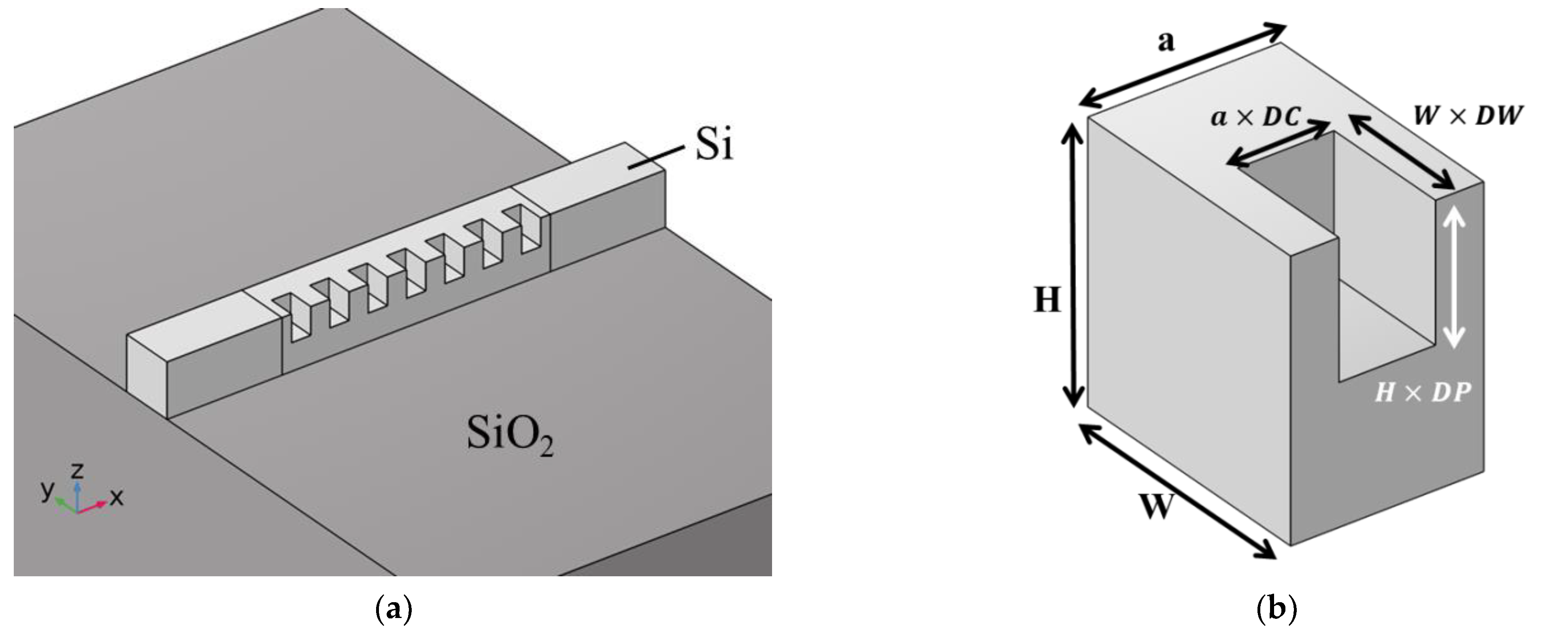
2. Materials and Methods
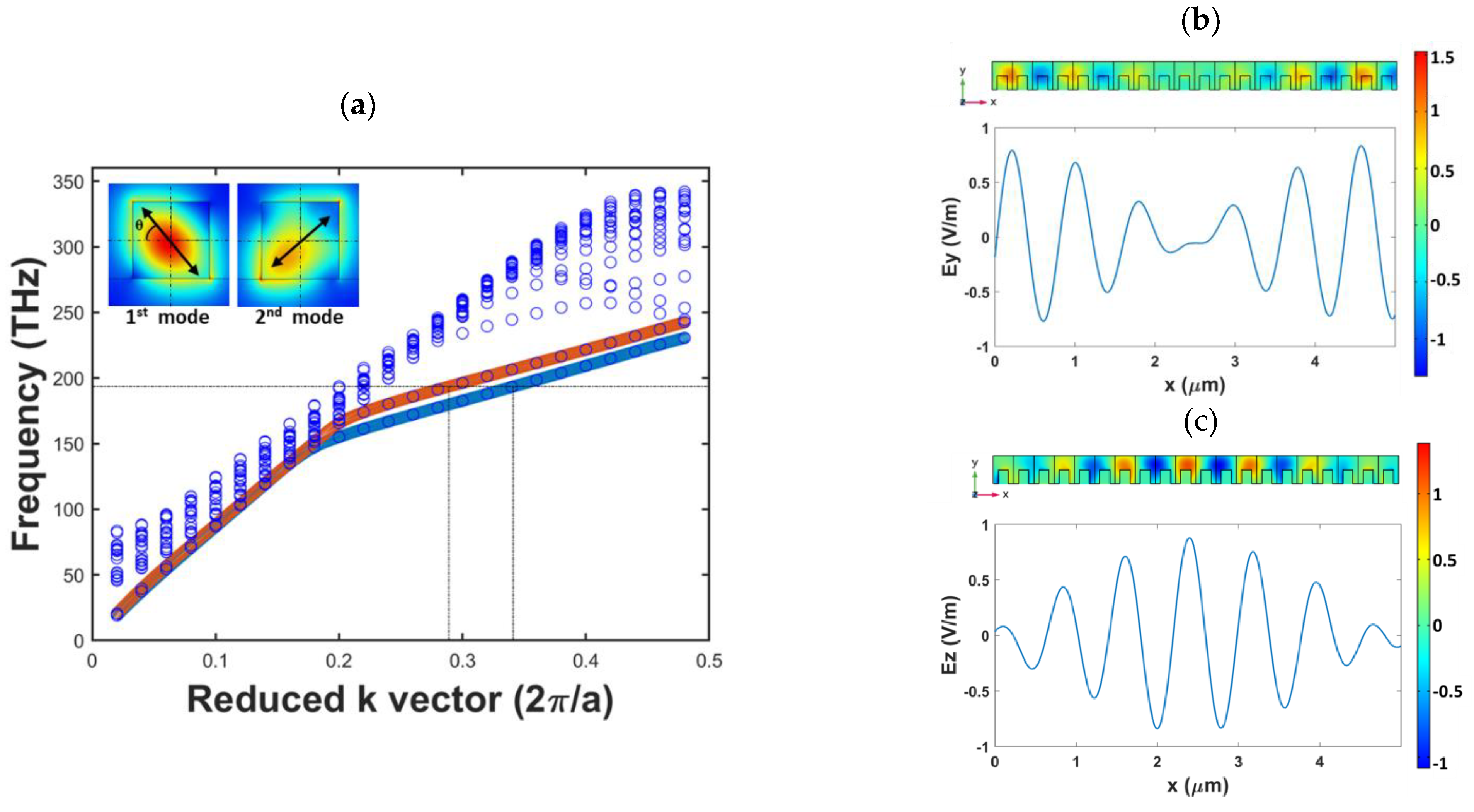
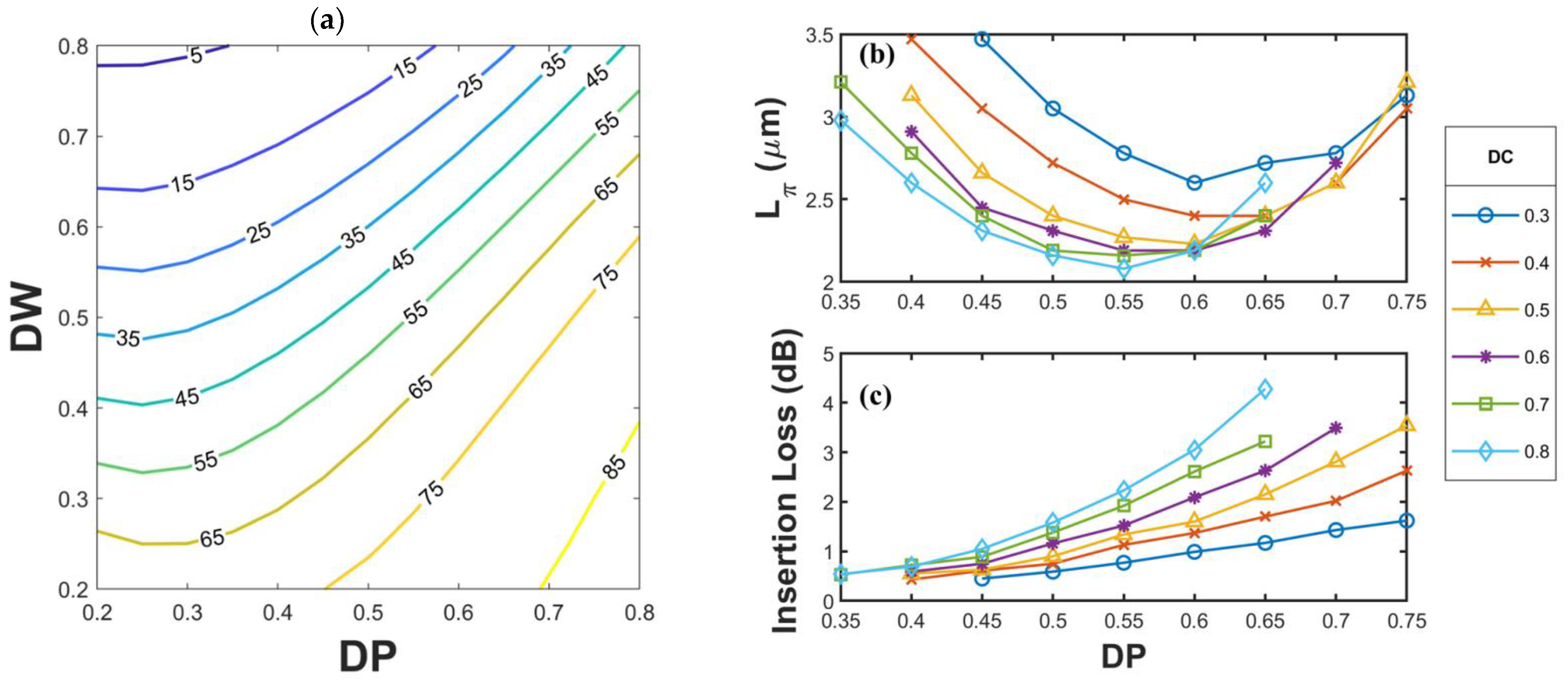
A schematic of the structure of the photonic crystal waveguide is displayed in Figure 1. We used an air cube array on one side of the square waveguide to form a tooth-shaped waveguide, as shown in Figure 1a. A SiO2 substrate (dark gray area in Figure 1) was placed below the waveguide. The waveguide (light gray area in Figure 1) consisted of square waveguides at the front and back for guiding electromagnetic waves and a tooth-shaped multi-period waveguide. These waveguides were made of Si and placed beneath an air layer that occupied the space above (not illustrated here). The refractive indices of SiO2, Si, and air were set as 1.46, 3.46, and 1, respectively. Figure 1b depicts a unit cell and the detailed structural parameters of the periodic tooth-like structures, where a is the lattice constant, H is the height of the waveguide, and W is the width of the waveguide. We defined the thickness, depth, and width of the air cube in the waveguide as a × DC, H × DP, and W × DW, respectively. To maintain the asymmetry of the waveguide’s cross section (similar to an L-shape), we limited DC, DP, and DW to 0.2–0.8.
We used the finite-element method (FEM) to simulate the light transmission behaviors and the photon band structures in the full structure. Band structures and light transmission behaviors were determined using eigenmode analysis and frequency–domain analysis, respectively. In the calculation of the eigenmode, we only used a unit cell with a width of a (Figure 1b). The band structure diagram of the photonic crystal was calculated by setting Floquet periodic boundary conditions in the x-direction, and the deviation angle of the optical axis of the wave plate was determined from the electric field data for the eigenmode. In addition, the polarization transition state and IL values of the full structure were analyzed in the frequency domain by plotting the full structure of the waveplate (Figure 1a). This structure contained multi-period tooth-shaped waveguides and complete square waveguides at its head and tail. An electromagnetic wave with a wavelength of 1.55 μm and y-polarization was incident onto the square waveguide from the x-direction, and it entered the tooth-shaped waveplate structure after passing through a complete square waveguide.

3. Results

We first selected the structure with DC = DP = DW = 0.5 for analysis and used the unit cell displayed in Figure 1b to obtain the band structure diagram of the photonic crystal through FEM-based eigenvalue calculation (Figure 2a). The horizontal axis of the band structure diagram in Figure 2a represents the reduced k-vector. The unit of this vector is 2π/a, and it represents the reciprocal space coordinates in the reduced Brillouin zone. The vertical axis of the aforementioned diagram denotes the eigenfrequency. The points in Figure 2a, which carry different k-vectors, represent the eigenfrequencies at specific k vectors. By connecting those points with similar field distributions, we found several lines in the band structure diagram, which represent the eigenmodes existing in the corresponding structure. We increased the number of data points in the two modes with the lowest frequency by using the interpolation method, and these modes are indicated using blue and orange lines in Figure 2a. The operating frequency was set as the frequency corresponding to a light wave with a vacuum wavelength of 1.55 μm (approximately 194 THz), which is marked with a dotted line Figure 2a. The photonic crystal structure corresponds to the two eigenmodes at the operating frequency, and the k-vectors in these eigenmodes had values of 0.289 (second mode, orange line) and 0.341 (first mode, blue line). After substituting the lattice constant a and wavelength into the reduced k-vector unit noted previously, the refractive index of the first and second modes were obtained (ns = 2.114 and nf = 1.792). We defined the optical axis of the first mode as the slow axis and that of the second mode as the fast axis. The electric field diagrams of the two modes are presented in the insets of Figure 2a.
Because the wave incident from the square waveguide exhibits TE or TM polarization, the half-wave-plate conditions must be fulfilled to achieve conversion between the two orthogonal linear polarization modes. According to the birefringence properties of a half-wave-plate, a phase difference Γ = 2 π · Δ n · L λ 0 = π exists between the components of the incident wave transmitted along the fast and slow axes. In the aforementioned equation, Δ n represents the differences in the refractive indices of the fast and slow axes, L represents the polarization rotation length, and λ 0 represents the wavelength of an incident wave in vacuum. According to the formula, the polarization rotation length can be found that is inverse proportional to Δ n at certain wavelength. Therefore, increasing the difference of the refractive indices between eigenmodes can produce shorter L. After substituting the two effective refractive indices of the guided modes and the vacuum wavelength of 1.55 μm into the aforementioned equation, the required polarization rotation length for the photonic crystal half-wave-plate was obtained as 2.41 μm (Lπ = λ0/(2∙∆n) = 2.41 μm). It can be noticed that it should be a reciprocal result when the light comes from the other side of the device due to the same modes. To verify this result, we performed frequency–domain analysis with a 20-period full structure. The electric field distribution and electric field intensity obtained when a y-polarized electromagnetic wave was transmitted along the waveguide are illustrated in Figure 2b,c, respectively. The electric field intensity map in the lower parts of Figure 2b,c reveals that Ey (intensity along the y-axis) was almost 0 at x = 2.45 μm. Moreover, at this point, Ez (intensity along the z-axis) reached its maximum value. The aforementioned results indicate that the analyzed structure converted y-polarized waves to z-polarized waves at a minimum distance of approximately 2.45 μm, which is close to the theoretical value obtained using the photonic band structure diagram.
For better understanding of the birefringence properties of a PhC-type wave plate structure, we calculated the optical axis deviation angle of the photonic crystal wave plate. By using the y- and z-component strengths of the electric field of the eigenmode to integrate the waveguide cross section Ω, the angle θ between the optical axis and the coordinate axis of mode can be defined as follows [19]:
tan θ = Ω n S i 2 ( y , z ) · E z 2 ( y , z ) d y d z Ω n S i 2 ( y , z ) · E y 2 ( y , z ) d y d z
where nSi is the refractive index of Si (i.e., 3.46).
The inset of Figure 2a shows the optical axis deviation angle θ in the first mode when DC = DP = DW = 0.5. Using Equation (1), we obtained θ   to   be   49.7 ° . Because of the presence of a SiO2 substrate under the waveguide, even when the cross section of the waveguide had a symmetric pattern with x = y as the axis of symmetry, the asymmetric material distribution around the waveguide caused the included angle of the optical axis to not be 45°. According to the characteristics of a half-wave-plate, when the phase difference between the waves passing along the fast and slow axes of a birefringent element is π, the angle φ between the original polarization direction and the optical axis is rotated to 2φ after these waves are linearly polarized and pass through the element. To achieve conversion between TE and TM polarization, 2φ should be 90°; therefore, a birefringent structure should be designed to have a φ value of 45° (i.e., θ = 45° is angle between the optical axis and the coordinate axis). To design a structure with θ = 45°, we calculated the optical axis deviation angle θ for the first mode according to the structural parameters DC, DP, and DW. Figure 3a displays the contour map drawn for DC = 0.5. The gradient of the contours in this figure exhibits an increasing trend from the upper left to the lower right, and the 45° contour is very close to the diagonal where DP = DW. The aforementioned figure reveals that when DP < 0.4, the slope of the contours gradually decreases, and the gradient distribution gradually shifts to the vertical direction; when the DP value is changed, the DW difference corresponding to the same optical axis angle is not very large. The 45° contour line has a high overlap with the DP = DW line only when DP > 0.6.
We extracted the part with L π < 3.5 μm from all the DP and DW combinations on the 45° contour line with different DC values, and the corresponding DC, DP, and DW values are listed in Table 1. On the basis of the structural parameters presented in Table 1, Lπ and IL were plotted for different components (Figure 3b,c). The term Lπ was calculated using the refractive index difference obtained through eigenvalue analysis. To determine the IL, tooth-shaped structures with lengths corresponding to the lengths of each structure (Lπ) were drawn (e.g., for DC = 0.4, DP = 0.4, and DW = 0.46, Lπ = 3.47 μm, which is approximately 13.88 times the value of a (=0.25 μm), and the tooth-shaped structure was drawn for 14 periods). The connected square waveguides in the front and back side of the tooth-shaped region are five periods long, and a y-polarized electromagnetic wave was incident from the x-direction of the square waveguide. The IL can be obtained from the output signal Eout and incident signal Ein received from the output end of the square waveguide as follows:
I L ( dB ) = 10 × log 10 E i n E o u t
It can be noticed that the formula in Equation (2) is similar to the polarization conversion efficiency. The polarization conversion efficiency is defined as the ratio between the output Ez field and the input Ey field, which will show an inverse proportional tendency with the IL. Due to the mechanism of the half-wave plate, the electric field can be almost totally converted to the target component except for the energy loss. The output electric fields in the other two components (i.e., Ex and Ey) are confirmed as one order smaller than the target component Ez. Therefore, we discuss Lπ with IL in the following θ = 45° structures.
Each line in Figure 3b,c represents a different DC value, and DP is the horizontal axis of this graph. For θ = 45°, the smallest value of Lπ (i.e., 2.08 μm) appeared when DC = 0.8, DP = 0.55, and DW = 0.55. The smallest IL (i.e., 0.43 dB) appeared when DC = 0.4, DP = 0.4, and DW = 0.46. If considering the applications in quantum communications, such a low IL device will be needed. According to the acceptable loss in the system, the relation shown in Figure 3b,c can provide several choices.
Figure 3b reveals that, at different DC values, the minimum value of Lπ appeared when 0.5 < DP < 0.6, with corresponding DW values falling in the range of 0.50–0.65. The trend in Figure 3c reveals that the IL increased with the DP value. If the DP value was between 0.5 and 0.6, the smallest Lπ value was obtained, and the IL was not too high. When DC increased, Lπ decreased; however, the rate of decrease of Lπ reduced when DC > 0.5. As displayed in Figure 3c, an increase in the DC value resulted in an increase in the IL because an increase in the DC value increased the size of the air cubes and caused energy dissipation into air. In summary, the DC value must be controlled within a certain range to shorten Lπ without increasing the IL substantially.
For DP values of 0.5–0.6, the Lπ values of each structure were very close to each other. Therefore, suitable geometry parameters could be selected within an appropriate Lπ range to reduce the IL. For example, when DP = 0.6 and DC > 0.5, the required polarization rotation length (Lπ) of each element was approximately 2.19 μm. A structure with DC = 0.5 had a low IL of 1.6 dB.
Finally, to find the optimal result among many parameter combinations, we plotted the product of the IL and Lπ (Figure 4) and determined the combination corresponding to the smallest IL and shortest conversion length. Figure 3c and Figure 4 exhibit similar trends, with the overall performance being better when the DC and DP values were small. However, the minimum value of the aforementioned product (1.49) appeared when DC = 0.4, DP = 0.4, and DW = 0.46 (indicated by the arrow), which indicates that a structure with a smaller DC value should be selected to reduce the IL to the greatest extent allowed by Lπ. Similarly, structures with smaller DP and DW values exhibit lower IL. The inset in Figure 4 illustrates the distribution of the electric field at the point indicated by the arrow, and the inset reveals that the Ey field in this structure (DC = 0.4, DP = 0.4, and DW = 0.46) was completely converted into an Ez field after passing through the photonic crystal wave plate, which confirmed the effectiveness of this structure.

4. Conclusions

In this study, we designed a waveguide-type waveplate based on one-dimensional photonic crystals and created a tooth-shaped waveguide on one side of a square waveguide with an air cube array. On the basis of the birefringence of the half-wave-plate, we used the band structure diagram to analyze the polarization rotation length of the PhC-type wave plate structure. We then verified the calculation results through the frequency–domain simulation of the full structure of the wave plate. By using the electric field data for the eigenmode, we calculated the deviation angle of the optical axis of the crystal. We found that when DP < 0.4, the DW values required to maintain a fixed rotation angle were all very close. This enhances the error tolerance in the fabrication process. By analyzing the effect of variations in the geometric parameters of the air cubes on θ, we found that structures with different geometric parameters at θ = 45° can have an Lπ value of less than 3.5 μm and an IL of less than 5 dB. The product of Lπ and IL confirmed that the designed photonic crystal wave plate exhibits superior overall performance when the air cubes have a smaller volume. When designing components, the required parameters can be effectively selected according to the Lπ and IL values provided by us. The proposed structure can be fabricated by two steps of E-Beam lithography and inductively coupled plasma dry etching processes. For the first step, the patterns of air squares can be defined by E-Beam lithography and etched by dry etching. For the second step, the waveguides’ pattern can be defined by E-Beam lithography with alignment key and etched by dry etching process. According to the Lπ or IL relations as a function of DP, DW, and DC shown above, the geometric parameters of the air cube can provide the fabrication tolerance to a certain extent. Finally, by adjusting the included angle of the optical axis of the wave plate structure, this structure can be used in designing waveguide-type polarization rotation devices.

Author Contributions

F.-L.H.: conceptualization, formal analysis, funding acquisition, methodology, project administration, supervision, writing—review and editing; C.-Y.N.: data curation, software, validation, writing—original draft; Y.-P.T.: data curation, formal analysis, methodology, project administration, software, validation, writing—original draft; T.-W.C.: formal analysis, investigation; Y.-T.Y.: investigation, resources; C.-J.F.: investigation, writing—review and editing; H.-M.C.: resources, writing—review and editing; C.-C.C. (Chien-Chung Chen): visualization; H.-F.L.: visualization; B.-S.L.: conceptualization, formal analysis, funding acquisition, methodology, project administration, supervision, writing—review and editing; K.-C.C.: formal analysis, investigation; C.-C.C. (Chii-Chang Chen): conceptualization, methodology, supervision. All authors have read and agreed to the published version of the manuscript.

Funding

This research received no external funding.

Data Availability Statement

Not applicable.

Conflicts of Interest

The authors declare that they have no known competing financial interest or personal relationships that could have appeared to influence the work reported in this paper.

References

  1. Headland, D.; Withayachumnankul, W.; Yamada, R.; Fujita, M.; Nagatsuma, T. Terahertz multi-beam antenna using photonic crystal waveguide and Luneburg lens. APL Photonics 2018, 3, 126105. [Google Scholar] [CrossRef] [Green Version]
  2. Martínez, A.; Míguez, H.; Griol, A.; Martí, J. Experimental and theoretical analysis of the self-focusing of light by a photonic crystal lens. Phys. Rev. B 2004, 69, 165119. [Google Scholar] [CrossRef]
  3. Roux, F.S.; De Leon, I. Planar photonic crystal gradient index lens, simulated with a finite difference time domain method. Phys. Rev. B 2006, 74, 113103. [Google Scholar] [CrossRef]
  4. Xie, J.; Wang, J.; Ge, R.; Yan, B.; Liu, E.; Tan, W.; Liu, J. Multiband super-resolution imaging of graded-index photonic crystal flat lens. J. Phys. D Appl. Phys. 2018, 51, 205103. [Google Scholar] [CrossRef]
  5. Chen, C.C.; Tsai, Y.L.; Hsu, C.L.; Chang, J.Y. Propagation loss reduction of photonic crystal slab waveguides by microspheres. Opt. Express 2004, 12, 3934–3939. [Google Scholar] [CrossRef] [PubMed]
  6. Chiu, W.Y.; Wu, Y.S.; Chan, Y.J.; Wang, T.D.; Hou, C.H.; Chien, H.T.; Chen, C.-C. Monolithically integrated photonic-crystal devices with photodiodes. Opt. Commun. 2011, 284, 4749–4751. [Google Scholar] [CrossRef]
  7. Dai, Q.F.; Li, Y.W.; Wang, H.Z. Broadband two-dimensional photonic crystal wave plate. Appl. Phys. Lett. 2006, 89, 061121. [Google Scholar] [CrossRef]
  8. Osinski, M.; Bayat, K.; Henneberger, F.; Chaudhuri, S.K.; Safavi-Naeini, S.; Arakawa, Y. Design and simulation of an ultra compact integrated wave plate using photonic crystal slab waveguide. In Proceedings of the Physics and Simulation of Optoelectronic Devices XV; SPIE: Bellingham, WA, USA, 2007. [Google Scholar]
  9. Sun, K.; Li, J.; Sun, J.; Ge, L.; Xu, D.; Zhong, K.; Yao, J. A high-performance terahertz back-reflections blocker based on wire grid and metasurface quarter-wave plate. Results Phys. 2022, 33, 105183. [Google Scholar] [CrossRef]
  10. Mennea, P.L.; Clements, W.R.; Smith, D.H.; Gates, J.C.; Metcalf, B.J.; Bannerman, R.H.S.; Burgwal, R.; Renema, J.J.; Kolthammer, W.S.; Walmsley, I.A.; et al. Modular linear optical circuits. Optica 2018, 5, 1087–1090. [Google Scholar] [CrossRef]
  11. Sanchis, L.; Håkansson, A.; López-Zanón, D.; Bravo-Abad, J.; Sánchez-Dehesa, J. Integrated optical devices design by genetic algorithm. Appl. Phys. Lett. 2004, 84, 4460–4462. [Google Scholar] [CrossRef] [Green Version]
  12. Matsuda, N.; Le Jeannic, H.; Fukuda, H.; Tsuchizawa, T.; Munro, W.J.; Shimizu, K.; Yamada, K.; Tokura, Y.; Takesue, H. A monolithically integrated polarization entangled photon pair source on a silicon chip. Sci. Rep. 2012, 2, 817. [Google Scholar] [CrossRef] [PubMed] [Green Version]
  13. O’Brien, J.L.; Furusawa, A.; Vučković, J. Photonic quantum technologies. Nat. Photonics 2009, 3, 687–695. [Google Scholar] [CrossRef] [Green Version]
  14. Politi, A.; Cryan, M.J.; Rarity, J.G.; Yu, S.; O’Brien, J.L. Silica-on-Silicon Waveguide Quantum Circuits. Science 2008, 320, 646–649. [Google Scholar] [CrossRef] [PubMed] [Green Version]
  15. Xiong, X.; Zou, C.L.; Ren, X.F.; Guo, G.C. Integrated polarization rotator/converter by stimulated Raman adiabatic passage. Opt. Express 2013, 21, 17097–17107. [Google Scholar] [CrossRef]
  16. Frey, B.J.; Leviton, D.B.; Madison, T.J. Temperature-dependent refractive index of silicon and germanium. In Optomechanical Technologies for Astronomy; SPIE: Bellingham, WA, USA, 2006; Volume 6273. [Google Scholar] [CrossRef] [Green Version]
  17. Fukuda, H.; Yamada, K.; Tsuchizawa, T.; Watanabe, T.; Shinojima, H.; Itabashi, S.-I. Polarization rotator based on silicon wire waveguides. Opt. Express 2008, 16, 2628–2635. [Google Scholar] [CrossRef]
  18. Holmes, B.M.; Hutchin, D.C. Realization of novel low-loss monolithically integrated passive waveguide mode converters. IEEE Photonics Technol. Lett. 2006, 18, 43–45. [Google Scholar] [CrossRef]
  19. Kim, S.-H.; Takei, R.; Shoji, Y.; Mizumoto, T. Single-trench waveguide TE-TM mode converter. Opt. Express 2009, 17, 11267. [Google Scholar] [CrossRef]
  20. Rahman, B.M.A.; Obayya, S.; Somasiri, N.; Rajarajan, M.; Grattan, K.T.V.; El-Mikathi, H.A. Design and Characterization of Compact Single-Section Passive Polarization Rotator. IEEE/OSA J. Lightw. Technol. 2001, 19, 512–519. [Google Scholar] [CrossRef]
  21. Jing, Z.; Mingbin, Y.; Guo-Qiang, L.; Dim-Lee, K. Silicon-Waveguide-Based Mode Evolution Polarization Rotator. IEEE J. Sel. Top. Quantum Electron. 2010, 16, 53–60. [Google Scholar] [CrossRef]
  22. Watts, M.R.; Haus, H.A. Haus. Integrated mode-evolution-based polarization rotators. Opt. Lett. 2005, 30, 138–140. [Google Scholar] [CrossRef]
  23. Yamauchi, J.; Yamanoue, M.; Nakano, H. A Short Polarization Converter Using a Triangular Waveguide. J. Lightwave Technol. 2008, 26, 1708–1714. [Google Scholar] [CrossRef] [Green Version]
  24. Wakabayashi, Y.; Hashimoto, T.; Yamauchi, J.; Nakano, H. Short Waveguide Polarization Converter Operating Over a Wide Wavelength Range. J. Lightwave Technol. 2013, 31, 1544–1550. [Google Scholar] [CrossRef]
  25. Wang, Z.; Dai, D. Ultrasmall Si-nanowire-based polarization rotator. J. Opt. Soc. Am. 2008, 25, 747–753. [Google Scholar] [CrossRef]
  26. Xie, A.; Zhou, L.; Chen, J.; Li, X. Efficient silicon polarization rotator based on mode-hybridization in a double-stair waveguide. Opt. Express 2015, 23, 3960–3970. [Google Scholar] [CrossRef] [PubMed] [Green Version]
  27. Chen, C.-C. Design of ultra-short polarization convertor with enhanced birefringence by photonic crystals. Results Phys. 2021, 24, 104138. [Google Scholar] [CrossRef]
Figure 1. Schematics of the (a) full structure and (b) unit cell of the photonic crystal waveplate.
Nanomaterials 12 02454 g001
Figure 2. (a) Band structure diagram (the insets display the electric field distributions of the first and second modes), (b) distribution and intensity maps of the y-component electric field, and (c) distribution and intensity maps of the z-component electric field of the structure with DC = 0.5, DP = 0.5, and DW = 0.5.
Nanomaterials 12 02454 g002
Figure 3. (a) Contour map of the optical axis deviation angle when DC = 0.5, (b) polarization rotation length, and (c) IL when θ = 45°.
Nanomaterials 12 02454 g003
Figure 4. Product of the polarization rotation length and IL when θ = 45° (the inset depicts the electric field distribution at the minimum value of this product).
Nanomaterials 12 02454 g004
Table 1. Structural parameters when θ = 45° and L π < 3.5 μm.
DP0.350.400.450.500.550.600.650.700.75
DW
DC
0.3 0.500.550.600.630.670.730.77
0.4 0.460.500.550.580.630.670.720.76
0.5 0.450.500.540.570.610.660.700.75
0.6 0.450.500.530.560.610.650.70
0.70.430.450.490.530.570.610.65
0.80.430.450.480.520.550.600.65
Publisher’s Note: MDPI stays neutral with regard to jurisdictional claims in published maps and institutional affiliations.

