Article

High Gas Sensitivity to Nitrogen Dioxide of Nanocomposite ZnO-SnO2 Films Activated by a Surface Electric Field

by
Victor V. Petrov
1,*,
Alexandra P. Ivanishcheva
1,*,
Maria G. Volkova
2,
Viktoriya Yu. Storozhenko
2,
Irina A. Gulyaeva
1,
Ilya V. Pankov
3,
Vadim A. Volochaev
3,
Soslan A. Khubezhov
4,5,6 and
Ekaterina M. Bayan
2
1
Institute of Nanotechnologies, Electronics, and Equipment Engineering, Southern Federal University, 347928 Taganrog, Russia
2
Department of Chemistry, Southern Federal University, 344090 Rostov-on-Don, Russia
3
Institute of Physical and Organic Chemistry, Southern Federal University, Stachki Av. 194/2, 344090 Rostov-on-Don, Russia
4
Research Laboratory of Functional Nanomaterials Technology, Southern Federal University, Shevchenko St. 2, 344006 Taganrog, Russia
5
Department of Nanophotonics and Metamaterials, ITMO University, 197101 St. Petersburg, Russia
6
Department of Physics, North-Ossetian State University, Vatutina Str. 46, 362025 Vladikavkaz, Russia
*
Authors to whom correspondence should be addressed.
Nanomaterials 2022, 12(12), 2025; https://doi.org/10.3390/nano12122025
Submission received: 12 May 2022 / Revised: 9 June 2022 / Accepted: 10 June 2022 / Published: 12 June 2022
(This article belongs to the Special Issue Nanomaterials in Gas Sensors)

Abstract

:
Gas sensors based on the multi-sensor platform MSP 632, with thin nanocomposite films based on tin dioxide with a low content of zinc oxide (0.5–5 mol.%), were synthesized using a solid-phase low-temperature pyrolysis technique. The resulting gas-sensitive ZnO-SnO2 films were comprehensively studied by atomic force microscopy, Kelvin probe force microscopy, X-ray diffraction, scanning electron microscopy, transmission electron microscopy, scanning transmission electron microscopy, energy dispersive X-ray spectrometry, and X-ray photoelectron spectroscopy. The obtained films are up to 200 nm thick and consist of ZnO-SnO2 nanocomposites, with ZnO and SnO2 crystallite sizes of 4–30 nm. Measurements of ZnO-SnO2 films containing 0.5 mol.% ZnO showed the existence of large values of surface potential, up to 1800 mV, leading to the formation of a strong surface electric field with a strength of up to 2 × 10⁷ V/cm. The presence of a strong surface electric field leads to the best gas-sensitive properties: the sensor’s responsivity is between two and nine times higher than that of sensors based on ZnO-SnO2 films of other compositions. A study of characteristics sensitive to NO2 (0.1–50 ppm) showed that gas sensors based on the ZnO-SnO2 film demonstrated a high sensitivity to NO2 with a concentration of 0.1 ppm at an operating temperature of 200 °C.

Graphical Abstract

1. Introduction

Gas sensors based on thin-film semiconductor oxide materials are widely used due to their high sensitivity to toxic gases [1,2,3]. Metal oxides, such as tin dioxide [4], zinc oxide [5], titanium dioxide [6], cobalt oxide [7], iron oxide [8], indium oxide and others [9] are used as gas-sensitive sensor materials for monitoring the concentration of pollutants (NOx, CO [10]) or process gases (H2S, H2, C3H8, C2H5OH, CH3COCH3, etc. [11]). Currently of great scientific interest are the gas-sensitive properties of metal oxide nanostructure (nanotubes, nanorods, nanofilms, nanowires, etc.) materials [12,13,14].
However, despite the good gas-sensitive properties of these materials, nanostructure synthesis technology is quite difficult to apply widely in the production of gas sensors. On the other hand, thin films of nanocomposite materials are used to determine low concentrations of gases (fractions and ppm units). Excellent results are shown by thin films based on tin dioxide, with the addition of other oxides in small concentrations [9,15,16,17,18] or heterostructures [19,20]. In this case, the nature, the oxidation degree, the crystallites size, and the modifying agents’ concentration are the controlling factors of the density of surface defects and the surface area of oxide nanomaterials [21], as well as the concentration of surface oxygen [15,22]. In such materials, ZnO-ZnO, SnO2-SnO2 homostructures, and ZnO-SnO2 heterojunctions, as well as Schottky barriers, are formed [23]. The resulting heterojunctions lead to an improvement in the gas-sensitive properties of nanocomposite materials [24].
Nanocomposite materials based on SnO2 are obtained by various methods [22], such as magnetron sputtering methods [25], chemical technologies [26,27,28], atomic layer deposition [29], the microwave hydrothermal method [30,31], magnetron sputtering [32], spray [33,34,35] or solid-phase [36,37] pyrolysis, etc. During the preparation of this article, the authors analyzed the available publications devoted to the study of the gas-sensitive and physicochemical properties of composite materials based on SnO2 with a small concentration of ZnO. A literature review shows that changes in the physicochemical and gas-sensitive properties of the obtained materials are significantly influenced by the concentration of the introduced additives.
The most important measuring results for nanocomposite ZnO-SnO2 films are shown in Table 1. It was found that better sensitive properties are recorded when the particle size of the gas-sensitive material is below 20–30 nm [23,29,38,39,40,41,42]. If crystallite size is higher, the sensitivity is usually lower [43,44,45]. On the other hand, the best gas-sensitive properties are shown for materials with the one component concentration equal to 10% or lower [15,29,46]. The first case can be explained by the existence of a depletion–enrichment zone comparable to the size of nanoparticles. In the second case, the situation is not fully explained. The authors of these publications, as a rule, explain a sensitivity increase by citing the presence of ZnO-SnO2 heterojunctions, the nanocrystalline structure, and the synergistic effect.
Additionally, there is an insufficient number of studies concerned with the influence of small concentrations of some metal oxides. The mechanism of gas sensitivity in such cases should be investigated comprehensively using X-ray photoelectron spectroscopy (XPS) [47] and high-resolution transmission electron microscopy (TEM, HRTEM).
Thus, the aim of the present work was to study the effect of small concentrations of zinc oxide (0.5–5 mol.%) on the physicochemical, electrophysical, and gas-sensitive properties of ZnO-SnO2 thin films. A new method of solid-phase pyrolysis was used to obtain gas-sensitive materials based on ZnO-SnO2 thin films. The characteristics of a gas sensor with ZnO-SnO2 films deposited on the MSP 632 multi-sensor platform (Heraeus Sensor Technology, Hanau, Germany) were also investigated.

2. Materials and Methods

2.1. Chemicals for Synthesis of ZnO-SnO2 Thin Films

Zinc acetate dihydrate (Zn(CH3COO)2·2H2O), stannic chloride pentahydrate (SnCl4·5H2O), an abietic acid (C19H29COOH), and 1,4-dioxane as a solvent were used as precursors for the synthesis of SnO2-ZnO thin films. The reagents were purchased from “ECROS”, Saint Petersburg, Russia. All chemicals used were of analytical grade or of the highest purity available.

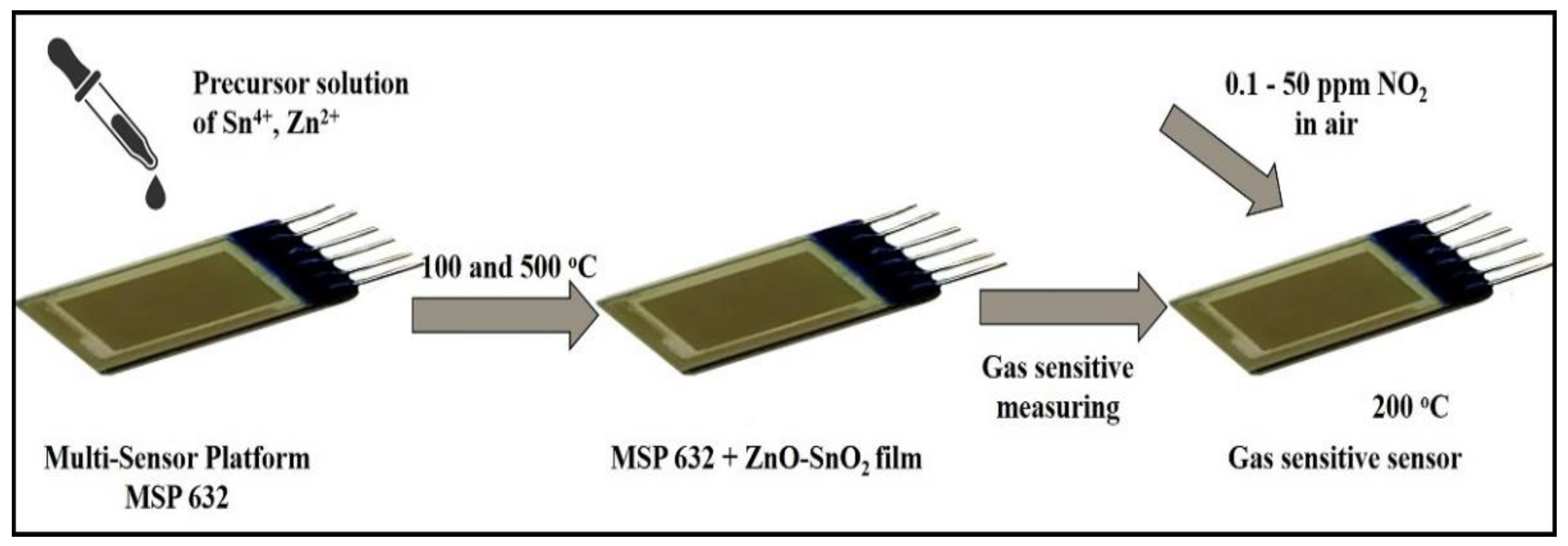
2.2. Synthesis of ZnO-SnO2 Thin Films

The synthesis was carried out in two stages. In the first stage, synthesis was carried out in a melt of abietic acid. The necessary amounts of zinc and tin salts were added to the melt, after which the melt was cooled and crushed. In the second stage, the necessary amounts of organic salts were dissolved in 1,4-dioxane so that the molar ratios of tin and zinc were Zn:Sn = 0:100 (sample 0ZnO), 0.5:99.5 (sample 0.5ZnO), 1:99 (sample 1ZnO), and 5:95 (sample 5ZnO) mol.%, respectively. The resulting solution was applied three times onto polycor substrates and a multi-sensor platform. The precursor solution was deposited on the multi-sensor platform using a mechanical pipette. Each layer was dried in air and in a drying cabinet at a temperature of 100 °C. Heat treatment was carried out at 500 °C for two hours (Figure 1). The synthesis technique is described in more detail in previous studies [15,36].
To make gas sensors based on ZnO-SnO2 thin films, precursor was applied over a Pt counter-pin structure multi-sensor platform, MSP 632, and dried at 100 °C. Annealing at a temperature of 500 °C for two hours in air- and temperature-controlled conditions was carried out directly, using a heater and a temperature sensor MSP 632.

2.3. Characterization
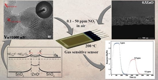
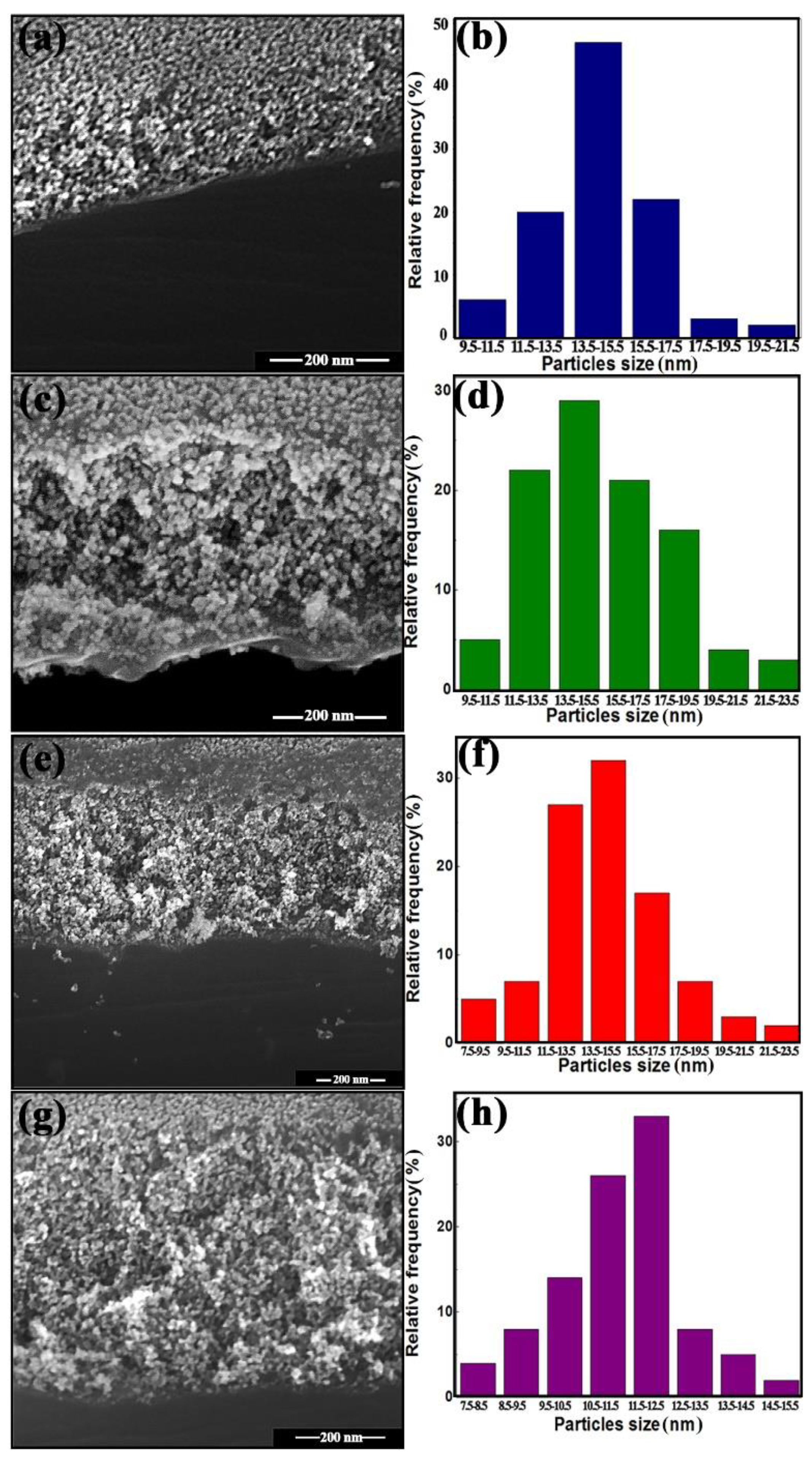
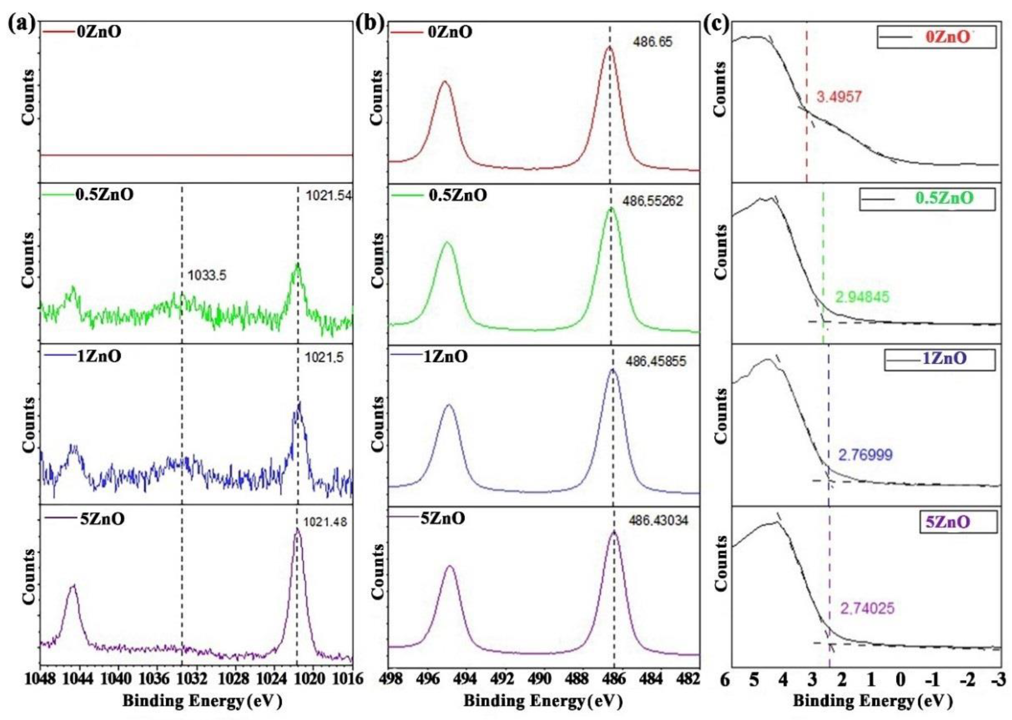
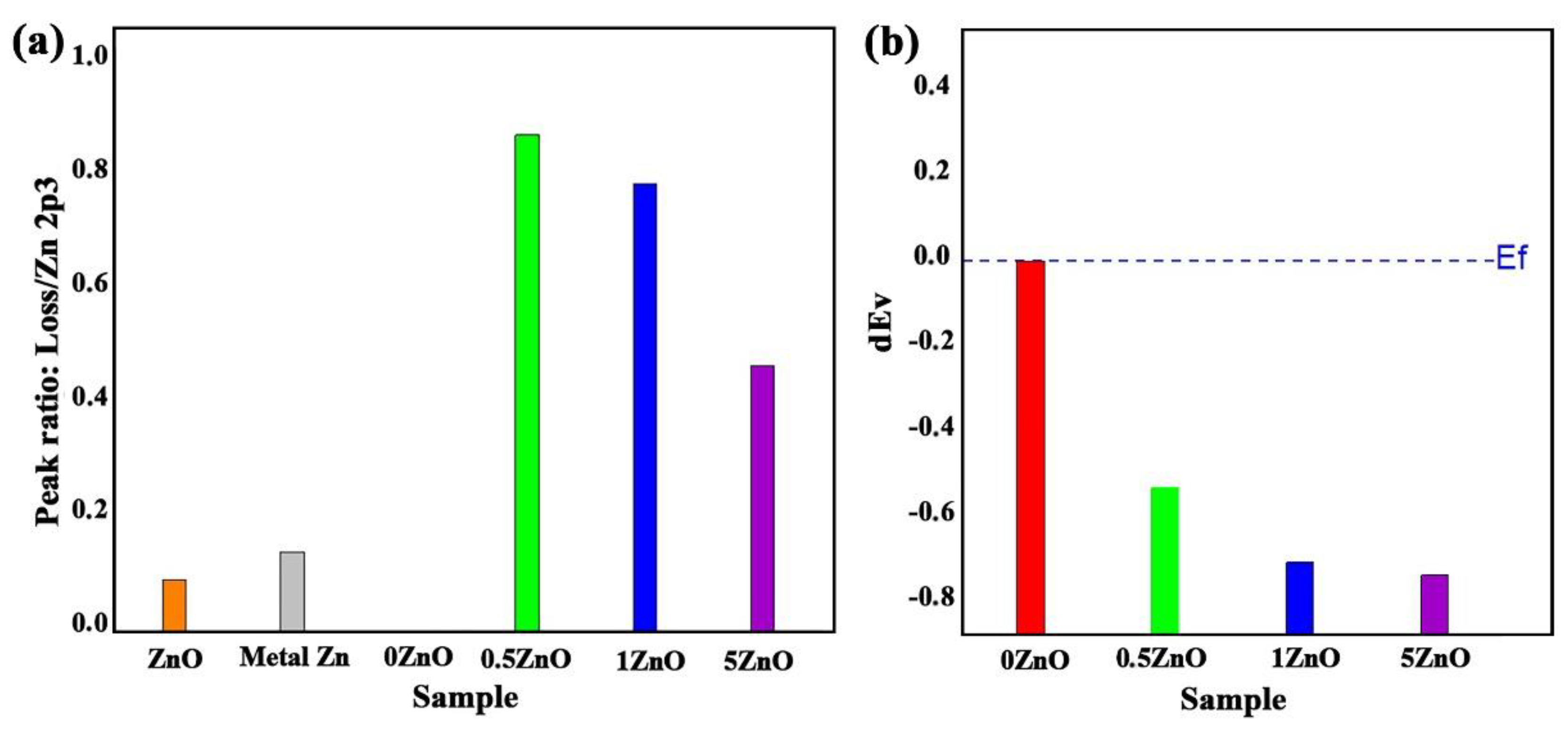
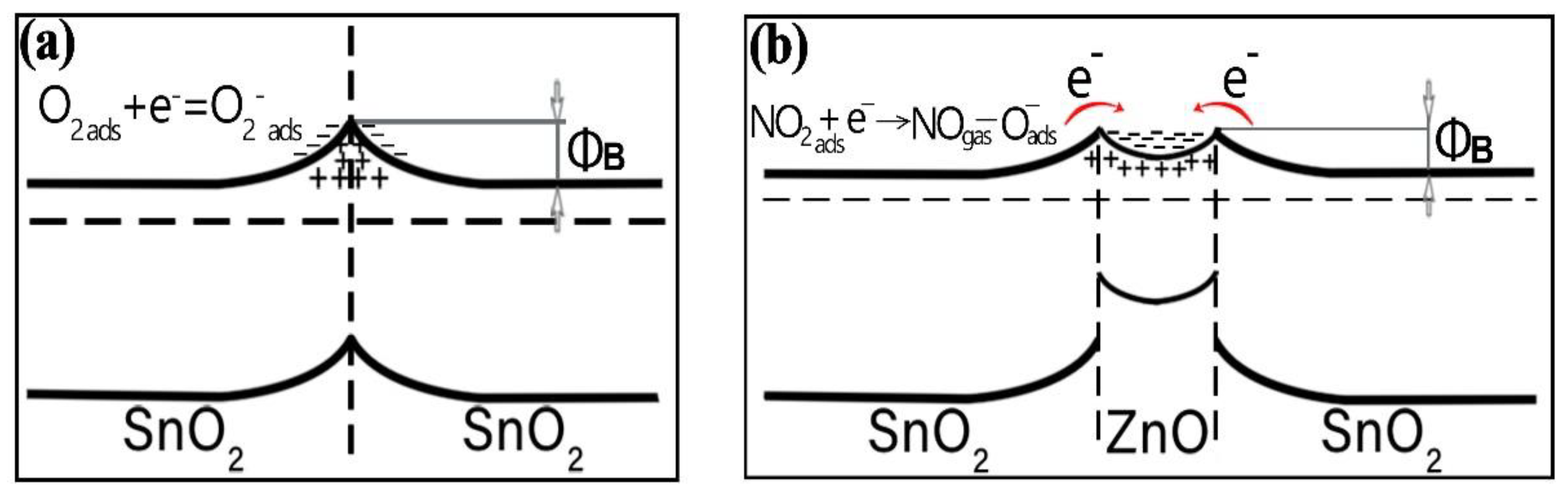
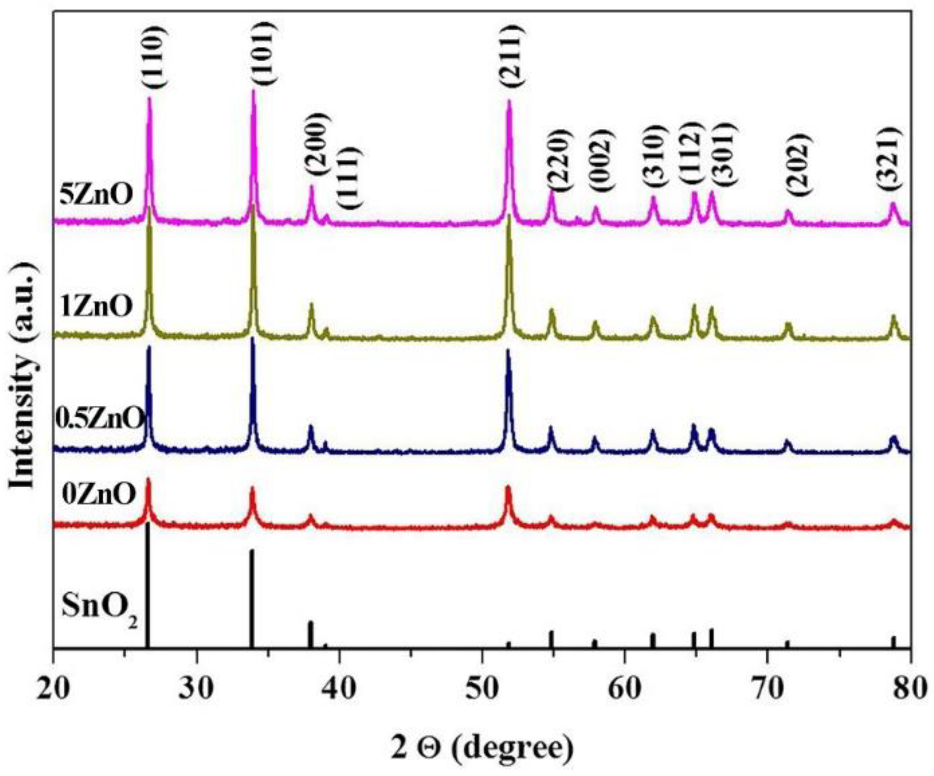
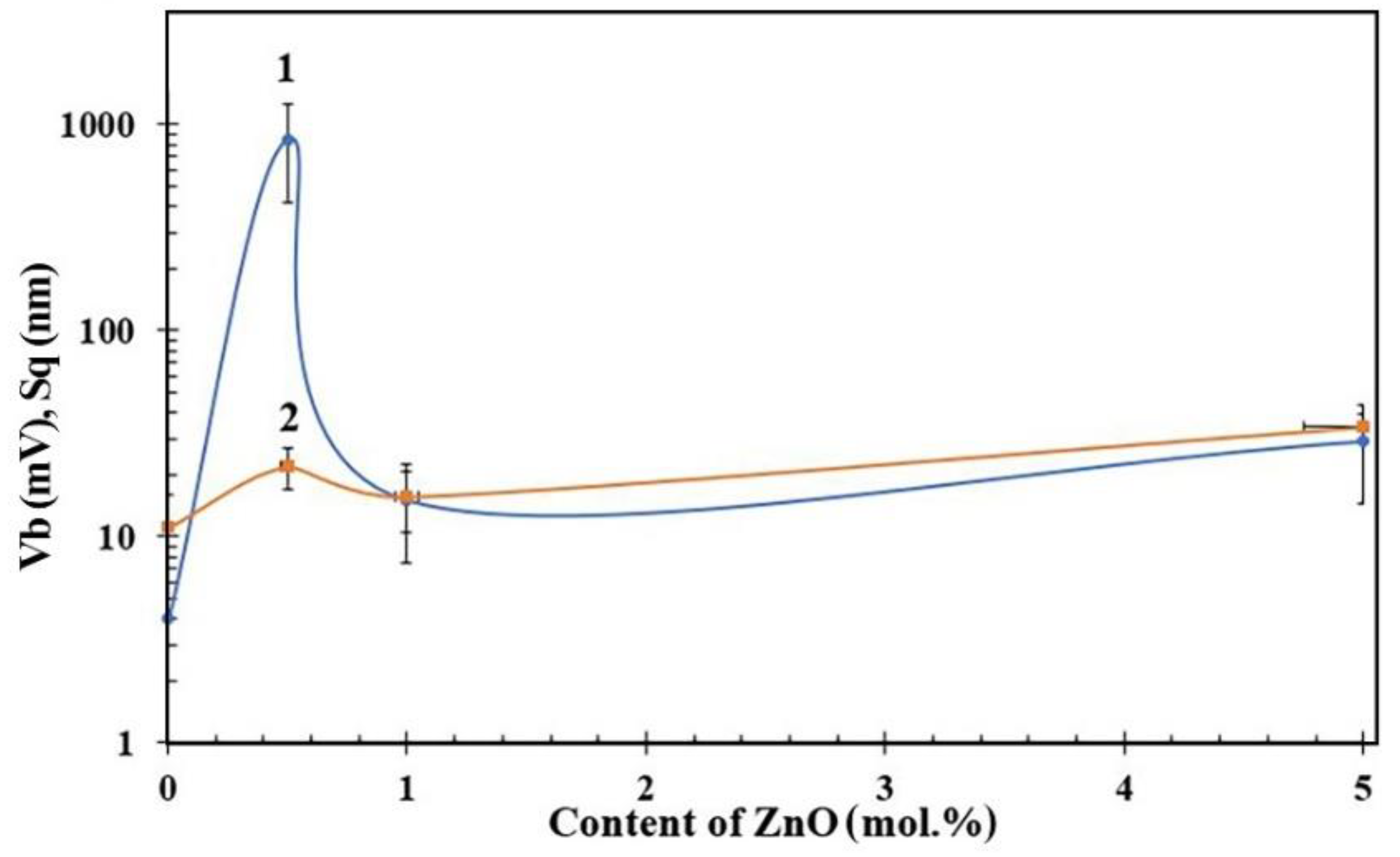
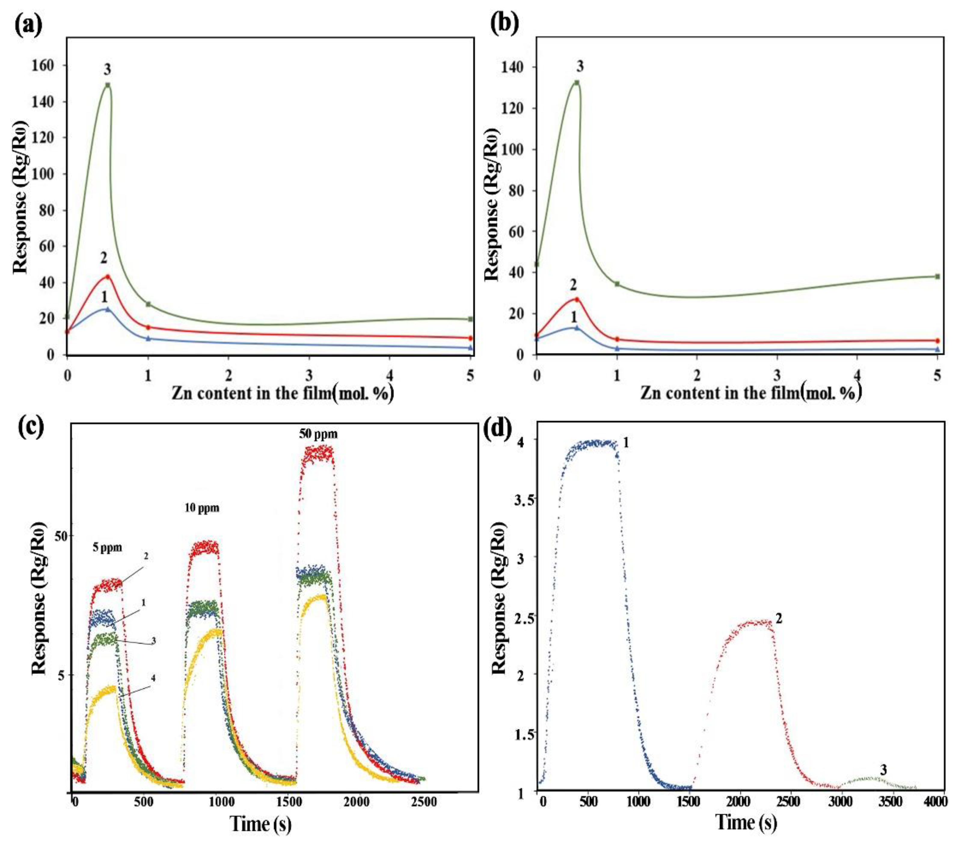
The resulting gas-sensitive ZnO-SnO2 films were comprehensively studied by atomic force microscopy (AFM), Kelvin probe force microscopy (KPFM), X-ray diffraction (XRD), scanning electron microscopy (SEM), transmission electron microscopy (TEM), scanning transmission electron microscopy (STEM), energy dispersive X-ray spectrometry (EDS), and XPS.
Electrophysical (volt-ampere characteristics; temperature dependences of electrical conductivity) and gas sensitivity measurements were estimated using an automated installation for determining the parameters of gas sensors [16]. In addition, the activation energy of conductivity (Ea) was estimated using the Arrhenius equation (Equation (1)) [48]:
G = G0 exp(−Ea/k∙T)
where k is the Boltzmann constant, and G0 the coefficient taking into account the bulk material conductivity.
Next, the temperature-stimulated conduction measurements [16,49,50] method was used to evaluate the “effective” value of the energy barrier between the grains of a nanocrystalline material.
The gas response of sensors was measured with 5–50 ppm nitrogen dioxide (NO2) balanced with synthetic air at operating temperatures of 200–250 °C. In the experiments, cylinders with test synthetic air and a mixture of synthetic air and NO2 (Monitoring LLC, Saint Petersburg, Russia) were used. The gases were injected at a flow rate of 0.3 dm3/min using a gas mixture generator (Microgaz F, Moscow, Russia) [16]. The response of sensor elements based on ZnO-SnO2 films was calculated using the following formula (Equation (2)):
S = Rg/R0
where R0 and Rg are the sensors resistance in synthetic air and in a mixture of synthetic air and NO2, respectively. Subsequently, the gas sensor, which showed the best gas-sensitive properties, was tested for exposure to NO2 with a concentration of 0.1 to 1 ppm.

3. Results

The XRD spectra of pure and ZnO-SnO2 thin films are shown in Figure 2. All of the diffraction peaks are well indexed to the tetragonal structure of SnO2 typical for cassiterite (JCPDS: 41–1445), regardless of the amount of modifying agents. Moreover, no additional diffraction peaks of ZnO were observed, which may be due both to the small amount of it in the system and to the small size of the crystallites. No other impurity phases are observed in the XRD pattern. The XRD patterns for pure and ZnO-SnO2 materials show that the films have a polycrystalline microstructure.
The degree of material crystallinity was determined by XRD according to the method described in the paper [49,50]. It was found that an increase in the content of the introduced additives leads to an increase in the degree of materials’ crystallinity (57.2, 66.0, 67.0 and 67.4% for 0ZnO, 0.5ZnO, 1ZnO, and 5ZnO materials, respectively).
Cross-sectional and top-view SEM images of 0ZnO (a), 0.5ZnO (c), 1ZnO (e), and 5ZnO (g) thin films are presented in Figure 3. It was found that the films are cracked, homogenous, and uniform, with a continuous distribution of grains. The type of coating obtained is an area with adjacent grains, and the thickness of the three-layer films is 160–240 nm; statistical processing of the results of the SEM analysis is shown in the histograms below. However, in SEM images, as a rule, it is difficult to determine the dimensions of agglomeration of observed nanocrystallites. Therefore, the sizes of nanocrystallites measured may, in this case, be partly overestimated.
The 0.5ZnO thin film was investigated using the TEM method. The synthesized film material consists of many nanocrystallites with particles ranging in size from 4.5–11.5 nm (Figure 4a,e–h). Where the film is thin, SnO2 nanocrystallites are visible in large quantities; between these, separate ZnO nanocrystallites are located. Studies conducted using the EDX method showed that the proportion of zinc in the material, by weight, does not exceed 1% of the mass (Figure 4a–f). The mapping of the elements Zn, O, and Sn in one film’s area is shown in Figure 4b–d. It can be seen that the elements Sn, Zn, and O are evenly distributed throughout the material, without local agglomeration. The content of the elements Sn, Zn, and O is consistent with the relative amount of the elements Sn, Zn, and O in the initial solution. The TEM images show that ZnO crystallites make contact with SnO2 crystallites. To prove this, high resolution photos were taken; areas 1 and 2 are highlighted in Figure 4e,f. Area 2 comprises SnO2 nanocrystallites, which is confirmed by the EDX analysis. Area 1 consists of nanocrystallites of SnO2 and ZnO, which are uniformly distributed thoughout the area. Moreover, since there are significantly more SnO2 nanocrystallites, ZnO nanocrystallites make contact with SnO2 nanocrystallites.
To observe the planes of the crystal structure, images with high magnification were obtained for some sections of the film. One particle with a lattice fringe of 0.264 nm corresponds to the plane (002) of the ZnO hexagonal structure: it is shown in Figure 4h. Additionally, on this site there are areas in which it is possible to distinguish a lattice fringe of 0.334 nm, which corresponds to the plane (110) of the SnO2 rutile structure. Thus, it can be concluded that nanoparticles consist of ZnO and SnO2 crystals. Selected area electron diffraction (SAED) circles correspond to the (110), (101), (200), (211), and (112) crystal planes of SnO2.
AFM and KPFM images of 0ZnO, 0.5ZnO, 1ZnO, and 5ZnO films are presented in Figure 5.
AFM studies showed that the films have a granular structure, with a height difference of Sq of 10–35 nm (Figure 5 and Figure 6). In general, with a decrease in the content of ZnO in the film, the roughness decreases from 34 to 11 nm. However, the 0.5ZnO film surface has a higher roughness than the surface of the 0ZnO and 1ZnO films—see Figure 6 (curve 2).
KPFM studies have shown that a lowest average value of the surface potential (Figure 6 (curve 1)) of about 4 mV is characteristic of SnO2 film (Figure 5h). 1ZnO and 5ZnO films have similar average values of surface potential, equal to 15–30 mV (Figure 5b,d).
However, for 0.5ZnO film, a peak value of the surface potential is observed, the average value of which reaches 845 mV, and at some points on the surface the maximum value is 1824 mV; the difference between the maximum and minimum values of Vb could be 1642 mV (Figure 5f and Figure S2).
The samples’ surface composition (Table 2) was also calculated from high-resolution XPS spectra using relative sensitivity factors from the Scofield Library. The high-resolution spectra of Zn2p, Sn3d and the valence band are presented in Figure 7. It can be seen from Figure 7b that the photoelectronic line Sn 3d for the sample 0ZnO (red curve) corresponds to SnO2.
Minor changes in the maximum positions of the Sn 3d photoelectronic lines for samples containing ZnO suggest the formation of a special interface at the nanocomposite oxides’ surface, which leads to a decrease in the work function. Analysis of the XPS spectra valence band edge makes it possible to evaluate and determine in more detail both the change in the maximum of the valence band (VBM), and the band gap and the Fermi level position at the phase boundary [51,52,53,54]. The formation of this interface in the ZnO-SnO2 system can be confirmed by analysing the high-resolution Zn2p spectra (Figure 7a). At zinc concentrations of 0.5% and 1%, the shapes of the Zn2p photoelectronic lines are very different from the case of bulk ZnO (Figure S1). In the region of binding energies of 1033.5 eV, plasmon losses, which are inherent in metallic zinc, are visible; however, the position and shape of the Zn2p3 peak exclude the presence of metallic zinc. The ratio of peak intensities of Zn2p3 photoelectronic lines’ plasmon losses for the obtained samples, as well as a comparison for pure metallic and ZnO crystalline, is shown in Figure 8a. Thus, the presence of a gap between the Fermi level and the edge of the valence band on the one hand, and the features of Zn2p photoelectronic lines on the other, completely exclude the presence of metallic zinc in the synthesized nanocomposites. The peculiarity of the Zn2p photoelectronic lines here can be linked to the formation of an interface enriched with charge carriers at the phase boundary, which leads to inelastic scattering of photoelectrons on them, and the appearance of an intense peak of plasmon losses in the region of 1033.5 eV.
The values of the valence band edge from high-resolution XPS spectra close to the Fermi level are determined using a linear approximation of the background line and the useful signal. The intersection of the obtained lines determines the value of the valence band edge, shown in Figure 7c.
From the analysis of the valence band edge, the values of the change in the valence band maximum for each sample are obtained according to the well-known formula (Equation (3)) [55]:
Δ E = ( E Sn 3 d SnO 2 E VBM SnO 2 ) ( E Zn 2 p ZnO E VBM ZnO ) + Δ E CL
where Δ E CL = E Zn 2 p ZnO E Sn 3 d SnO 2 ;
E Sn 3 d SnO 2 binding   energy   of   3 d 5   electrons   in   SnO 2 ;
E VBM SnO 2 valence   band   edge   value   in   SnO 2
E Zn 2 p ZnO binding   energy   of   2 p 3   electrons   in   ZnO
E VBM ZnO valence   band   edge   value   in   в   ZnO
Valence band edge values and the binding energy of core levels for ZnO2p3/2 and SnO2 3d5/2 are presented in Table 3.
The distribution of the change in the valence band level at the interface for each sample is presented below in Figure 8b.
The dependence of reverse resistance on reverse temperature for all samples has a characteristic form for metal oxide semiconductors (Figure 9).
The activation energy of conductivity (Ea), calculated by the Arrhenius equation (Figure 9b, curve 1), shows a sharp (by 2–2.5 times) decrease in the Ea and the potential barrier ΦB for 0.5ZnO films. The Ea decreases from 0.51 eV to 0.2 eV, and the ΦB from 1.1 eV to 0.54 eV.
The results of the gas sensitivity study of ZnO-SnO2 films at 200 °C and 250 °C are shown in Figure 10. The typical response of gas sensors when exposed to NO2 with concentrations of 5, 10, and 50 ppm is shown in Figure 10c.
It is shown (Figure 10c) that, when exposed to NO2 concentrations of 5, 10, and 50 ppm, a gas sensor based on a 0.5ZnO-99.5SnO2 film is approximately 1.5–9 times more sensitive to NO2 compared to gas sensors based on ZnO-SnO2 films with other compositions. For exposure to NO2 with a concentration of 50 ppm and an exposure temperature of 200 °C, the sensor’s response S is equal to 146. The evaluation of the response time tresp shows (Table 4) that for this sensor, when exposed to 5 ppm NO2, tresp is 144 s and 80 s at operating temperatures of 200 and 250 °C, respectively.
A gas sensor based on a 0.5ZnO-99.5SnO2 film has a higher sensitivity; it was therefore investigated for exposure to NO2 with concentrations from 0.1 to 1 ppm. The sensor response of this gas sensor is shown in Figure 10d. The response value, when exposed to NO2 with a concentration of 1.0 ppm, is 3.9, and, when exposed to NO2 with a concentration of 0.1 ppm, is 1.1.
Thus, gas sensors based on a ZnO-SnO2 film, synthesized using a solid-phase pyrolysis technique with a ratio of 0.5ZnO, have a range of measured concentrations of NO2 equal to 0.1–50 ppm, with a response time of 80–144 s, and an operating temperature of 200 °C.
To test the selectivity of the sensor based on a 0.5ZnO-99.5SnO2 film to other gases, studies were conducted with acetone, ethanol, ammonia, and water molecules, with a concentration of 200 ppm at an operating temperature of 200 °C. The sensor response was 1.1 for acetone, 1.25 for ethanol, 1.76 for ammonia, and 1.1 for water. It can be seen that, in comparison with the response value for nitrogen dioxide with a concentration of 50 ppm (146), these values do not exceed 1.2%.

4. Discussion

It is known that the valence band edge for pure SnO2 is 3.5 eV [54,55]. This is also confirmed by our measurements for the material ZnO:SnO2 = 0:100 (Figure 8, Table 3). For 0.5ZnO film materials or for other ZnO-SnO2 materials, the energy level of the valence band edge decreases to 2.95 eV. Further decrease in the valence band edge value is slower—up to 2.77 and 2.74 eV for 1ZnO and 5ZnO materials, respectively. Thus, the energy of the valence band edge in ZnO-SnO2 films decreases with an increase in the ZnO concentration.
Potential barriers are formed at the interface of SnO2-SnO2 homostructures and the ZnO-SnO2 heterojunction. Measured by temperature-stimulated conduction measurements, the value of the potential barrier ΦB for the SnO2 film was 0.80 eV (Figure 9b). This potential barrier is formed due to the adsorption of oxygen molecules on the surface of SnO2 nanocrystals, and their subsequent ionization with the formation of O2 ions [33,56,57,58,59,60].
The contact of two SnO2 nanocrystallites is shown in Figure 11a. It is well known that, because of this contact, a depletion region is formed in SnO2 nanocrystallites [59,60,61].
The study of the gas sensor based on the film material 0.5ZnO-99.5SnO2 showed that the value of ΦB sharply decreases to 0.47 eV (Figure 9b). With a further increase in the ZnO concentration (1ZnO and 5ZnO), ΦB becomes significantly higher—1.1 and 1.0 eV, respectively. The mechanism of a sharp decrease in ΦB in the gas sensor based on the 0.5ZnO-99.5SnO2 film is shown in Figure 11b. It is known that the work function of ZnO (5.2–5.3 eV) [62,63] is higher than that of SnO2 (4.8–4.9 eV) [61,64]. In addition, the Fermi level of SnO2 is closer to the vacuum level, in relation to the Fermi level of ZnO. When ZnO and SnO2 crystallites are in contact with each other, electrons will transfer from tin dioxide to zinc oxide (Figure 11). The value of the potential barrier at the SnO2-ZnO-SnO2 heterojunction will decrease in this case (Figure 9b). According to TEM studies (Figure 4c), individual ZnO crystallites come into contact with SnO2 crystallites, so ZnO becomes highly enriched with charge carriers. This fact is also confirmed by XPS studies: plasmon losses are observed on Zn2p3 zinc photoelectronic lines (Figure 7a). The same effect leads to the appearance of regions with large local surface potential Vb. This is confirmed by our KPFM measurements (Figure 5c and Figure 6b). On the surface of the 0.5ZnO film, the average value of the surface potential is 845 mV, and in some places reaches values of 1824 mV (Figure 5c). For film materials with a higher content of zinc oxides (1ZnO and 5ZnO), the concentration of ZnO crystallites becomes higher, which leads to a decrease in the average value of the surface potential to 15–30 mV. The existence of high values of the Vb in 0.5ZnO-99.5SnO2 films leads to the formation of a strong surface electric field. The electric field contributes to the reduction of the ΦB between nanocrystallites. In this regard, Ea also decreases in the 0.5ZnO-99.5SnO2 film. In addition, it can be noted that the surface potential affects the morphology of the film’s surface (Figure 6).
As can be seen from Figure 10, gas sensors based on the film material 0.5ZnO-99.5SnO2 show a peak response to NO2 exposure, compared to other samples.
The reason for this sharp increase in response may, on the one hand, be a decrease in the potential barrier ΦB [65]. On the other hand, however, the reason for the sharp increase in the response of gas sensors based on film material 0.5ZnO-99.5SnO2 is, in our opinion, the high surface potential formed due to the contact of ZnO and SnO2 crystallites. The analysis of TEM images (Figure 4) shows that the distance between the crystallites is no more than 0.1 nm. At such values, distances, and potentials, there is a surface electric field with a strength of 2 × 10⁷ V/cm. It is known that an electric field with a strength of up to 3 × 10⁷ V/cm can exist in oxide materials if their thickness is up to 4 nm [66,67]. The presence of a surface electric field is supported by the response decreasing from 200 °C to 250 °C (Figure 10a,b), since it is well known that an increase in temperature leads to a decrease in the influence of the electric field. The effect of the electric field influence on the atoms’ diffusion over the surface, and in the volume of solids, has been well studied [68,69].
As shown in [70], the surface electric field of this magnitude, created by charged adsorption centers, significantly affects the mechanism of the interaction of polar gas molecules with the gas-sensitive material’s surface.
It is known that the NO2 molecule has a dipole moment 0.29–0.33 D [71,72,73]. In this case, the interaction energy of the polar adsorbate molecule with the charged adsorption center (Qaa) can be estimated using the following formula (Equation (4)) [74]:
Q aa = N a × e × V × μ z 0 2
where e is the electron charge; V is the valence of the adsorbent ion; μ is the dipole moment of the adsorbate molecule; z0 is the equilibrium distance between the adsorbate molecule and the charged adsorption centre; and Na is the Avogadro constant.
Calculations show that if z0 is equal to 0.2 nm, the Qaa for the NO2 molecule is 31–35 kJ/mol.
At the same time, we have shown that a sufficiently strong surface electric field (Es), of magnitude (1–2) × 107 V/cm, is created at the crystallite boundary of tin and zinc oxides. The processes of adsorption and dissociation of NO2 molecules are activated by a strong surface electric field. NO2 molecules receive an additional field-induced dipole moment (µi), the magnitude of which depends on the polarizability of the α molecule. It is known that the NO2 molecule has a high polarizability (α), equal to 1.8 × 10⁻²⁴ cm3 [67].
When the amount of polarizability increases, the surface electric field effect on the molecule also increases. The energy of the adsorbate–adsorbent interaction (Qaa) increases by the value of the induction component (Qi) associated with the occurrence of the induced dipole moment. The value of µi can be estimated using the formula (Equation (5)) [75].
μi = α × Es.
Calculation of the total dipole moment (μ′ = μ + µi) shows that μ′ can be equal to 0.47–0.51 D.
In addition, the adsorbate molecule will be affected by orientation polarization, in accordance with the direction of the electric field, which depends on the magnitude of the molecule’s dipole moments [75]. The energy of the orientation influence (Qor) of the field is equal to (Equation (6)):
Qor = 0.5 × μ′ × Es,
The total energy of the adsorbate adsorbent (Qaa′) interaction between the adsorption centre and the NO2 molecule is calculated by the formula (Equation (7)):
Qaa′ = (Qaa + Qi + Qor).
The calculation results show that, for an NO2 molecule with high polarizability, the Qaa′ can increase to 57–60 kJ/mol, that is, almost twofold. Such energy may already be enough to initiate the process of dissociation of gas molecules, since the activation energy of the molecule’s dissociation is half of the molecule dissociation energy [76,77]. The latter circumstance means that dissociation of the NO2 molecule is possible. These arguments do not contradict previously published works [78,79]. Thus, adsorption of NO2 molecules, with their subsequent dissociation, can occur (Equation (8)):
N O 2 , g a s + e N O 2 , a d s O a d s + N O g a s ,
A strong surface electric field is a powerful activating factor, as is ultraviolet radiation. In the presence of these factors, forced ionization of adsorbed molecules can occur (Equation (9)) [80]:
N O 2 g a s + O 2 + 2 e N O 2 + 2 O
As can be seen, these reactions can lead to a stronger response to NO2 molecules.
A comparative analysis of the gas sensitivity to NO2 of nanocomposite ZnO-SnO2 structures presented in Table 1 and in this paper shows that the size of nanostructures (nanocrystallites) is essential for high gas sensitivity to low concentrations of NO2 in the air. In all works, the nanostructures of the gas-sensitive material are formed by different technologies, and have sizes from 5 to 17 nm [15,29,30,40,41,42]. In addition, when the operating temperature of the gas sensor decreases, the response and recovery times increases [30,81]. The optimal value of the operating temperatures for sensors with low concentrations of nitrogen dioxide is, in our opinion, in the range of 150–250 °C, in order to achieve the optimal value of response times of 80–140 s. When analyzing these articles, the gas-sensitive properties of sensors based on ZnO-SnO2 films are similar.
The characteristics of NO2 sensors based on other materials are presented in Table 5.
Sensors operating at room temperature have long response/recovery times [82,83,84,89,90,91,92,93]. The advantage of such sensors is that there is no need for heating to operating temperature, and they can be used indoors. Since gas sensors are used for NO2 monitoring outside, in a wide temperature range, sensors operating at 200 °C are recommended for analysis unification. Sensors with response/recovery times in the range of 30–180 s have a more complex technology for forming a gas-sensitive layer [86,87,88,93]. Some gas-sensitive materials are unstable over time, in particular metal sulfides [83,85,86].
Thus, it can be seen that many materials used in gas sensors of the resistive type have similar gas-sensitive characteristics. The choice of gas-sensitive materials is determined by the following requirement: “simple technology—high-quality, reproducible and fast response to a given concentration.” The solid-phase pyrolysis method proposed in this work and in our other works [15,36] satisfies this requirement. Using the described method, it is possible to obtain composite nanoscale materials of various compositions with high values of gas-sensitive characteristics. In this case, by selecting the composition of mixed ZnO-SnO2 oxides, this technology allows for the formation of heterostructures with a strong surface electric field, thereby “fine-tuning” the gas-sensitive properties.

5. Conclusions

Nitrogen dioxide gas sensors were formed on the MSP 632 multi-sensor platform. The gas-sensitive element of the sensor is a ZnO-SnO2 film with thickness 60–200 nm. The film materials were formed using a new low-temperature pyrolysis technique; the zinc oxide content was from 0.5 to 5 mol.%.
Comprehensive studies of the materials’ physicochemical, structural, electrophysical, and other properties were carried out using modern research methods. It was shown that all ZnO-SnO2 films are composite with crystallite sizes of 4–30 nm and have a cassiterite structure. Zinc oxide nanocrystallites are evenly distributed in the structure of ZnO-SnO2 films.
This leads to the creation, in the 0.5ZnO-99.5SnO2 film, of a surface potential of up to 1800 mV. This is because of the existence of a strong surface electric field with a strength of (1–2) × 107 V/cm.
When NO2 molecules approach the surface of the ZnO-SnO2 film, a strong surface electric field promotes the induction of a dipole moment in the molecule. As a result, this leads to an increase in the energy of the adsorbate–adsorbent interaction between the adsorption center and the NO2 molecule, and an activation of the molecules’ dissociation process. The response of the gas sensor based on 0.5ZnO film is 1.5–9 times higher compared to sensors based on other ZnO-SnO2 films.
Thus, it was shown that the gas sensor based on film material 0.5ZnO-99.5SnO2 is very promising for the detection of NO2 gas at concentrations of 0.1–50 ppm; it has a response time equal to 80–144 s and an operating temperature of 200 °C.

Supplementary Materials

The following supporting information can be downloaded at https://www.mdpi.com/article/10.3390/nano12122025/s1, Figure S1: The XPS spectra of pure zinc and its oxide, Figure S2: Distribution of the surface potential on the film surface 0.5ZnO.

Author Contributions

V.V.P.: conceptualization, investigation, methodology, writing—review and editing, project administration, funding acquisition. A.P.I.: SEM, electrophysical and gas sensitive properties. M.G.V.: material synthesis, analysis of the XRD data, writing the Introduction. V.Y.S.: material synthesis. I.A.G.: AFM and KPFM analysis and gas sensitive properties. I.V.P.: TEM and STEM analysis. V.A.V.: sample preparation for TEM, TEM analysis. S.A.K.: XPS analysis. E.M.B.: analysis of the data, investigation, methodology, writing the manuscript, review, and editing. The corresponding author, V.V.P., ensured that the descriptions are accurate and agreed by all authors. All authors have read and agreed to the published version of the manuscript.

Funding

This research was funded by the RFBR, project 20-07-00653.

Informed Consent Statement

Informed consent was obtained from all subjects involved in the study.

Data Availability Statement

Not applicable.

Acknowledgments

Electrophysics and gas sensitivity measurements were conducted using equipment from the Centre for Collective Use, Microsystem Technics and Integral Sensors, Southern Federal University (SFedU). The XPS analyses were carried out at the Nanophysics and Nanotechnology Research Center (CCU SOGU). We also thank the staff of the Laboratory for the Technology of Functional Nanomaterials at the Institute of Nanotechnologies, Electronics, and Equipment Engineering and SEC Nanotechnology (SFedU), Ageev O.A., Ilyin O.I. and Ilyina M.V., for providing the opportunity to conduct SEM, AFM, and KFPM research. The authors are grateful to the Shared Use Center’s High-Resolution Transmission Electron Microscopy (SFedU), which was used to conduct the TEM studies.

Conflicts of Interest

The authors declare no conflict of interest.

References

  1. Kim, H.J.; Lee, J.H. Highly sensitive and selective gas sensors using p-type oxide semiconductors: Overview. Sens. Actuators B Chem. 2014, 92, 607–627. [Google Scholar] [CrossRef]
  2. Li, Z.; Li, H.; Wu, Z.; Wang, M.; Luo, J.; Torun, H.; Hu, P.; Yang, C.; Grundmann, M.; Liu, X.; et al. Advances in designs and mechanisms of semiconducting metal oxide nanostructures for high-precision gas sensors operated at room temperature. Mater. Horiz. 2019, 6, 470–506. [Google Scholar] [CrossRef] [Green Version]
  3. Zhang, C.; Luo, Y.; Xu, J.; Debliquy, M. Room temperature conductive type metal oxide semiconductor gas sensors for NO2 detection. Sens. Actuators A Phys. 2019, 289, 118–133. [Google Scholar] [CrossRef]
  4. Mehraj, S.; Ansari, M.S. Annealed SnO2 thin films: Structural, electrical and their magnetic properties. Thin Solid Film. 2015, 589, 57–65. [Google Scholar] [CrossRef]
  5. Bayan, E.M.; Petrov, V.V.; Volkova, M.G.; Storozhenko, V.Y.; Chernyshev, A.V. SnO2-ZnO nanocomposite thin films: The influence of structure, composition and crystallinity on optical and electrophysical properties. J. Adv. Dielectr. 2021, 11, 2160008. [Google Scholar] [CrossRef]
  6. Kim, I.D.; Rothschild, A.; Lee, B.H.; Kim, D.Y.; Jo, S.M.; Tuller, H.L. Ultrasensitive Chemiresistors Based on Electrospun TiO2 Nanofibers. Nano Lett. 2006, 6, 2009–2013. [Google Scholar] [CrossRef]
  7. Xu, J.M.; Cheng, J.P. The advances of Co3O4 as gas sensing materials: A review. J. Alloys Compd. 2016, 686, 753–768. [Google Scholar] [CrossRef]
  8. Mirzaei, A.; Hashemi, B.; Janghorban, K. α-Fe2O3 based nanomaterials as gas sensors. J. Mater. Sci. Mater. Electron. 2016, 27, 3109–3144. [Google Scholar] [CrossRef]
  9. Velumani, M.; Meher, S.R.; Alex, Z.C. Composite metal oxide thin film based impedometric humidity sensors. Sens. Actuators B Chem. 2019, 301, 127084. [Google Scholar] [CrossRef]
  10. Mahajan, S.; Jagtap, S. Metal-oxide semiconductors for carbon monoxide (CO) gas sensing: A review. Appl. Mater. Today 2020, 18, 100483. [Google Scholar] [CrossRef]
  11. Yamazoe, N. Toward innovations of gas sensor technology. Sens. Actuators B Chem. 2005, 108, 2–14. [Google Scholar] [CrossRef]
  12. Korotcenkov, G. Current Trends in Nanomaterials for Metal Oxide-Based Conductometric Gas Sensors: Advantages and Limitations. Part 1: 1D and 2D Nanostructures. Nanomaterials 2020, 10, 1392. [Google Scholar] [CrossRef] [PubMed]
  13. Mendoza, F.; Hernández, D.M.; Makarov, V.; Febus, E.; Weiner, B.R.; Morell, G. Room temperature gas sensor based on tin dioxide-carbon nanotubes composite films. Sens. Actuators B Chem. 2014, 190, 227–233. [Google Scholar] [CrossRef]
  14. Chen, Y.J.; Nie, L.; Xue, X.Y.; Wang, Y.G.; Wang, T.H. Linear ethanol sensing of SnO2 nanorods with extremely high sensitivity. Appl. Phys. Lett. 2006, 88, 083105. [Google Scholar] [CrossRef]
  15. Petrov, V.V.; Sysoev, V.V.; Starnikova, A.P.; Volkova, M.G.; Kalazhokov, Z.K.; Storozhenko, V.Y.; Khubezhov, S.A.; Bayan, E.M. Synthesis, Characterization and Gas Sensing Study of ZnO-SnO2 Nanocomposite Thin Films. Chemosensors 2021, 9, 124. [Google Scholar] [CrossRef]
  16. Zhang, D.; Cao, Y.; Li, P.; Wu, J.; Zong, X. Humidity-sensing performance of layer-by-layer self-assembled tungsten disulfide/tin dioxide nanocomposite. Sens. Actuators B Chem. 2018, 265, 529–538. [Google Scholar] [CrossRef]
  17. Mohanta, D.; Ahmaruzzaman, M.D. Novel Ag-SnO2-βC3N4 ternary nanocomposite based gas sensor for enhanced low-concentration NO2 sensing at room temperature. Sens. Actuators B Chem. 2020, 326, 128910. [Google Scholar] [CrossRef]
  18. Xu, Y.; Zhang, W.; Liu, X.; Zhang, L.; Zhang, L.; Yang, C.; Pinna, N.; Zhang, J. Platinum single atoms on tin oxide ultrathin films for extremely sensitive gas detection. Mater. Horiz. 2020, 7, 1519–1527. [Google Scholar] [CrossRef]
  19. Ramos-Ramos, D.J.; Sotillo, B.; Urbieta, A.; Fernandez, P. Fabrication and Characterization of ZnO:CuO Electronic Composites for Their Application in Sensing Processes. IEEE Sens. J. 2021, 21, 2573–2580. [Google Scholar] [CrossRef]
  20. Zhang, S.; Liu, Z.; Zhang, L.; Chen, J.; Zho, Q.; Zhang, H.; Nie, L.; Don, Z.; Zhan, Z.; Wang, Z.; et al. Construction of a low-temperature, highly sensitive H2S sensor based on surfaces and interfaces reaction triggered by Au-doped hierarchical structured composites. Chem. Phys. Lett. 2021, 763, 138188. [Google Scholar] [CrossRef]
  21. Ha, N.H.; Thinh, D.D.; Huong, N.T.; Phuong, N.H.; Thach, P.D.; Hong, H.S. Fast response of carbon monoxide gas sensors using a highly porous network of ZnO nanoparticles decorated on 3D reduced graphene oxide. Appl. Surf. Sci. 2018, 434, 1048–1054. [Google Scholar] [CrossRef]
  22. Liangyuan, C.; Shouli, B.; Guojun, Z.; Dianqing, L.; Aifan, C.; Liu, C.C. Synthesis of ZnO-SnO2 nanocomposites by microemulsion and sensing properties for NO2. Sens. Actuators B Chem. 2008, 134, 360–366. [Google Scholar] [CrossRef]
  23. Katoch, A.; Kim, J.H.; Kwon, Y.J.; Kim, H.W.; Kim, S.S. Bifunctional Sensing Mechanism of SnO2-ZnO Composite Nanofibers for Drastically Enhancing the Sensing Behavior in H2 Gas. ACS Appl. Mater. Interfaces 2015, 7, 11351–11358. [Google Scholar] [CrossRef] [PubMed]
  24. Lia, T.; Zenga, W.; Wang, Z. Quasi-one-dimensional metal-oxide-based heterostructural gas-sensing materials: A review. Sens. Actuators B Chem. 2015, 221, 1570–1585. [Google Scholar] [CrossRef]
  25. Velumani, M.; Meher, S.R.; Alex, Z.C. Impedometric humidity sensing characteristics of SnO2 thin films and SnO2-ZnO composite thin films grown by magnetron sputtering. J. Mater. Sci. Mater. Electron. 2018, 29, 3999–4010. [Google Scholar] [CrossRef]
  26. Sin, N.D.M.; Ahmad, S.; Malek, M.F.; Mamat, M.H.; Rusop, M. Improvement sensitivity humidity sensor based on ZnO/SnO2 cubic structure. J. IOP Conf. Ser. Mater. Sci. Eng. 2013, 46, 012005. [Google Scholar] [CrossRef]
  27. Zhao, S.; Shen, Y.; Zhou, P.; Li, G.; Hao, F.; Han, C.; Liu, W.; Wei, D. Construction of ZnO-SnO2 n-n junction for dual-sensing of nitrogen dioxide and ethanol. Vacuum 2020, 18, 1109615. [Google Scholar] [CrossRef]
  28. Zhao, S.; Chen, Y.; Zhou, P.; Gao, F.; Xu, X.; Gao, S.; Wei, D.; Ao, Y.; Shen, Y. Enhanced NO2 sensing performance of ZnO nanowires functionalized with ultra-fine In2O3 nanoparticles. Sens. Actuator. B Chem. 2020, 308, 127729. [Google Scholar] [CrossRef]
  29. Zhao, B.; Mattelaer, F.; Kint, J.; Werbrouck, A.; Henderick, L.; Minjauw, M.; Dendooven, J.; Detavernier, C. Atomic layer deposition of ZnO-SnO2 composite thin film: The influence of structure, composition and crystallinity on lithium-ion battery performance. Electrochim. Acta 2019, 320, 134604. [Google Scholar] [CrossRef]
  30. Wang, Z.; Zhi, M.; Xu, M.; Guo, C.; Man, Z.; Zhang, Z.; Li, Q.; Lv, Y.; Zhao, W.; Yan, J.; et al. Ultrasensitive NO2 gas sensor based on Sb-doped SnO2 covered ZnO nano-heterojunction. J. Mater. Sci. 2021, 56, 7348–7356. [Google Scholar] [CrossRef]
  31. Lou, C.; Yang, C.; Zheng, W.; Liu, X.; Zhang, J. Atomic layer deposition of ZnO on SnO2 nanospheres for enhanced formaldehyde detection. Sens. Actuators B Chem. 2020, 329, 129218. [Google Scholar] [CrossRef]
  32. Al-Jumaili, H.S.; Jasim, M.N. Preparation And Characterization Of ZnO:SnO2 Nanocomposite Thin Films On Porous Silicon as H2S Gas Sensor. J. Ovonic Res. 2019, 15, 81–87. [Google Scholar]
  33. Sharma, B.; Sharma, A.; Joshi, M.J. Myung, Sputtered SnO2/ZnO Heterostructures for Improved NO2 Gas Sensing Properties. Chemosensors 2020, 8, 67. [Google Scholar] [CrossRef]
  34. Shewale, P.S.; Yu, Y.S.; Kim, J.H.; Bobade, C.R.; Uplane, M.D. H2S gas sensitive Sn-doped ZnO thin films: Synthesis and characterization. J. Anal. Appl. Pyrolysis 2015, 112, 348–356. [Google Scholar] [CrossRef]
  35. Srinivasulu, T.; Saritha, K.; Reddy, K.T.R. Synthesis, and characterization of Fe-doped ZnO thin films deposited by chemical spray pyrolysis. Mod. Electron. Mater. 2017, 3, 76–85. [Google Scholar] [CrossRef]
  36. Petrov, V.V.; Bayan, E.M.; Khubezhov, S.A.; Varzarev, Y.N.; Volkova, M.G. Investigation of Rapid Gas-Sensitive Properties Degradation of ZnO-SnO2 Thin Films Grown on the Glass Substrate. Chemosensors 2020, 8, 40. [Google Scholar] [CrossRef]
  37. Volkova, M.G.; Storozhenko, V.Y.; Petrov, V.V.; Bayan, E.M. Characterization of nanocrystalline ZnO thin films prepared by new pyrolysis method. J. Phys. Conf. Ser. 2020, 1695, 012023. [Google Scholar] [CrossRef]
  38. El Khalidi, Z.; Daouli, A.; Jabraoui, H.; Hartiti, B.; Bouich, A.; Soucase, B.M.; Comini, E.; Arachchige, M.M.; Fadili, S.; Thevenin, P.; et al. Impact of Sn doping on the hydrogen detection characteristics of ZnO thin films: Insights from experimental and DFT combination. Appl. Surf. Sci. 2022, 574, 151585. [Google Scholar] [CrossRef]
  39. Park, J.A.; Moon, J.; Lee, S.J.; Kim, S.H.; Chu, H.Y.; Zyung, T. SnO2-ZnO hybrid nanofibers-based highly sensitive nitrogen dioxides sensor. Sens. Actuators B Chem. 2010, 145, 592–595. [Google Scholar] [CrossRef]
  40. Liu, S.; Zhang, Y.; Gao, S.; Fei, T.; Zhang, Y.; Zheng, X.; Zhang, T. An organometallic chemistry-assisted strategy for modification of zinc oxide nanoparticles by tin oxide nanoparticles: Formation of n-n heterojunction and boosting NO2 sensing properties. J. Colloid Interface Sci. 2020, 567, 328–338. [Google Scholar] [CrossRef]
  41. Lu, G.; Xu, J.; Sun, J.; Yu, Y.; Zhang, Y.; Liu, F. UV-enhanced room temperature NO2 sensor using ZnO nanorods modified with SnO2 nanoparticles. Sens. Actuators B Chem. 2012, 162, 82–88. [Google Scholar] [CrossRef]
  42. Kim, K.W.; Cho, P.S.; Kim, S.J.; Lee, J.H.; Kang, C.Y.; Kim, J.S.; Yoon, S.J. The selective detection of C2H5OH using SnO2-ZnO thin film gas sensors prepared by combinatorial solution deposition. Sens. Actuators B Chem. 2007, 123, 318–324. [Google Scholar] [CrossRef]
  43. Mondal, B.; Basumatari, B.; Das, J.; Roychaudhury, C.; Saha, H.; Mukherjee, N. ZnO-SnO2 based composite type gas sensor for selective hydrogen sensing. Sens. Actuators B Chem. 2014, 194, 389–396. [Google Scholar] [CrossRef]
  44. Pakhare, K.S.; Sargar, B.M.; Potdar, S.S.; Sharma, A.K.; Patil, U.M. Facile Synthesis of Nano-Diced SnO2-ZnO Composite by Chemical Route for Gas Sensor Application. J. Electron. Mater. 2019, 48, 6269–6279. [Google Scholar] [CrossRef]
  45. Thanh Le, D.T.; Trung, D.D.; Chinh, N.D.; Thanh Binh, B.T.; Hong, H.S.; Van Duy, N.; Hoa, N.D.; Van Hieu, N. Facile synthesis of SnO2–ZnO core–shell nanowires for enhanced ethanol-sensing performance. Curr. Appl. Phys. 2013, 13, 1637–1642. [Google Scholar] [CrossRef]
  46. Lai, T.Y.; Fang, T.H.; Hsiao, Y.J.; Chan, C.A. Characteristics of Au-doped SnO2-ZnO heteronanostructures for gas sensing applications. Vacuum 2019, 166, 155–161. [Google Scholar] [CrossRef]
  47. Myasoedova, T.N.; Yalovega, G.E.; Shmatko, V.A.; Funik, A.O.; Petrov, V.V. SiO2CuOx films for nitrogen dioxide detection: Correlation between technological conditions and properties. Sens. Actuators B Chem. 2016, 230, 167–175. [Google Scholar] [CrossRef]
  48. Shalimova, K.V. Physics Semiconductors, 2nd ed.; Revised and Expanded, Energy; Scientific Research: Moscow, Russia, 1976. [Google Scholar]
  49. Korovkin, M.; AnanIeva, L.; Nebera, T.; Antsiferova, A. Assessment of quartz materials crystallinity by X-ray diffraction. IOP Conf. Ser. Mater. Sci. Eng. 2016, 110, 012095. [Google Scholar] [CrossRef] [Green Version]
  50. Murata, K.J.; Norman, M.B. An index of crystallinity for quartz. Am. J. Sci. 1976, 276, 1120–1130. [Google Scholar] [CrossRef]
  51. Vorobyeva, N.A.; Rumyantseva, M.N.; Forsh, P.A.; Gaskov, A.M. Conductivity of Nanocrystalline ZnO(Ga). Semiconductors 2013, 47, 650–654. [Google Scholar] [CrossRef]
  52. Clifford, P.K.; Tuma, D.T. Characteristics of Semiconductor Gas Sensors II. Transient Response to Temperature Change. Sens. Actuators B Chem. 1983, 3, 255–281. [Google Scholar] [CrossRef]
  53. Hunsicker, R.A.; Klier, K.; Gaffney, T.S.; Kirchner, J.G. Framework Zinc-Substituted Zeolites:  Synthesis, and Core-Level and Valence-Band XPS. Chem. Mater. 2002, 14, 4807–4811. [Google Scholar] [CrossRef]
  54. Fang, J.; Fan, H.; Ma, Y.; Wang, Z.; Chang, Q. Surface defects control for ZnO nanorods synthesized by quenching and their anti-recombination in photocatalysis. Appl. Surf. Sci. 2015, 332, 47–54. [Google Scholar] [CrossRef]
  55. Kraut, E.A.; Grant, R.W.; Waldrop, J.R.; Kowalczyk, S.P. Precise Determination of the Valence-Band Edge in X-Ray Photoemission Spectra: Application to Measurement of Semiconductor Interface Potentials. Phys. Rev. Lett. 1980, 44, 1620–1623. [Google Scholar] [CrossRef]
  56. Zhou, W.; Liu, Y.; Tang, Y.; Wu, P. Band Gap Engineering of SnO2 by Epitaxial Strain: Experimental and Theoretical Investigations. Phys. Chem. C 2014, 118, 6448–6453. [Google Scholar] [CrossRef]
  57. Ganose, A.M.; Scanlon, D.O. Band gap and work function tailoring of SnO2 for improved transparent conducting ability in photovoltaics. J. Mater. Chem. C 2016, 4, 1467–1475. [Google Scholar] [CrossRef] [Green Version]
  58. Henrich, V.E.; Cox, P.A. The Surface Science of Metal Oxides; Cambridge University Press: Cambridge, UK, 1993; p. 460. [Google Scholar]
  59. Bonasewicz, P.; Hirschwald, W.; Neumann, G. Influence of surface processes on electrical, photochemical, and thermodynamical properties of zinc oxide film. Electrochem. Soc. 1986, 133, 2270–2278. [Google Scholar] [CrossRef]
  60. Juna, J.H.; Yuna, J.; Choa, K.; Hwangb, I.-S.; Leeb, J.-H.; Kim, S. Necked ZnO nanoparticle-based NO2 sensors with high and fast response. Sens. Actuators B Chem. 2009, 140, 412–417. [Google Scholar] [CrossRef]
  61. Alosfur, F.K.M.; Ridha, N.J. Synthesis, and characterization of ZnO/SnO2 nanorods core-shell arrays for high performance gas sensors. Appl. Phys. A 2021, 127, 203. [Google Scholar] [CrossRef]
  62. Wei, M.; Li, C.F.; Deng, X.R.; Deng, H. Surface work function of transparent conductive ZnO films. Energy Procedia 2012, 16, 76–80. [Google Scholar] [CrossRef] [Green Version]
  63. Mishra, Y.; Chakravadhanula, V.; Hrkac, V.; Jebril, S.; Agarwal, D.; Mohapatra, S.; Avasthi, D.; Kienle, L.; Adelung, R. Crystal growth behaviour in Au-ZnO nanocomposite under different annealing environments and photoswitchability. Appl. Phys. 2012, 112, 064308. [Google Scholar] [CrossRef]
  64. Sahm, T.; Gurlo, A.; Barsan, N.; Weimar, U. Basics of oxygen and SnO2 interaction; work function change and conductivity measurements. Sens. Actuators B Chem. 2006, 118, 78–83. [Google Scholar] [CrossRef]
  65. Yamazoe, N.; Shimanoe, K. Roles of Shape and Size of Component Crystals in Semiconductor Gas Sensors: II. Response to NO2 and H2. Electrochem. Soc. 2008, 155, J93–J98. [Google Scholar] [CrossRef]
  66. Osburn, C.M.; Ormond, D.W. Dielectric breakdown properties in silicon dioxide films. Electrochem. Soc. 1972, 119, 591. [Google Scholar] [CrossRef]
  67. Harari, E. Dielectric Breakdown in electrically stressed thin Films of termal SiO2. Appl. Phys. 1978, 49, 2478. [Google Scholar] [CrossRef]
  68. Yasunaga, H.; Natori, A. Electromigration on semiconductor surfaces. Surf. Sci. Rep. 1992, 15, 205–280. [Google Scholar] [CrossRef]
  69. Korolev, A.N.; Sechenov, D.A.; Petrov, V.V. The nonlinear model of low temperature semiconductors impurity diffusion of direct electric field. Fiz. Khim. Obr. Mat. 1993, 5, 100. [Google Scholar]
  70. Petrov, V.V. Investigation of the gas molecules interaction features with the oxide gas-sensitive materials surface. Nano Microsyst. Technol. 2007, 1, 24–27. [Google Scholar]
  71. Kikoin, I.K. Tables of Physical Quantities; Guide; Atomizdat: Moscow, Russia, 1986. [Google Scholar]
  72. Grigoriev, I.E.; Meilikhov, E.Z. Physical Quantities; Guide; Energoatomizdat: Moscow, Russia, 1991. [Google Scholar]
  73. Nikolsky, B.P. Chemist’s Handbook (V.1), 2nd ed.; Reprint and Add, Chemistry; Goshimizdat: Moscow, Russia, 1976. [Google Scholar]
  74. Gerasimov, Y.I.; Dreving, V.P.; Eremin, E.N.; Kiselev, A.V.; Lebedev, V.P.; Panchenkov, G.M.; Shlygin, A.I. Physical Chemistry Course (V.1); Gerasimov, Y.I., Ed.; Chemistry: Moscow, Russia, 1964. [Google Scholar]
  75. Stromberg, A.G.; Semchenko, D.P. Physical Chemistry; Stromberg, A.G., Ed.; Higher School: Moscow, Russia, 1973. [Google Scholar]
  76. Henney, N. Solid State Chemistry; Mir: Moscow, Russia, 1971. [Google Scholar]
  77. Gerasimov, V.V.; Gerasimova, V.V.; Samoilov, A.G. Activation energy of the reaction in heterogeneous catalysis. Rep. USSR Acad. Sci. 1992, 332, 744–748. [Google Scholar]
  78. Francioso, L.; Forleo, A.; Capone, S.; Epifani, M.; Taurino, A.M.; Siciliano, P. Nanostructured In2O3-SnO2 sol-gel thin film as material for NO2 detection. Sens. Actuators B Chem. 2006, 114, 646–655. [Google Scholar] [CrossRef]
  79. Masa, S.; Robes, D.; Hontanon, E.; Lozano, J.; Eqtestadi, S.; Narros, A. Graphene-Tin Oxide Composite Nanofibers for Low Temperature Detection of NO2 and O3. Sens. Transducers 2020, 246, 71–78. [Google Scholar]
  80. Saboor, F.H.; Ueda, T.; Kamada, K.; Hyodo, T.; Mortazavi, Y.; Khodadadi, A.A.; Shimizu, Y. Enhanced NO2 gas sensing performance of bare and Pd-loaded SnO2 thick film sensors under UV-light irradiation at room temperature. Sens. Actuators B Chem. 2016, 223, 429–439. [Google Scholar] [CrossRef]
  81. Sharma, A.; Tomar, M.; Gupta, V. SnO2 thin film sensor with enhanced response for NO2 gas at lower temperatures. Sens. Actuators B Chem. 2011, 156, 743–752. [Google Scholar] [CrossRef]
  82. Popescu, M.; Simandan, I.D.; Sava, F.; Velea, A.; Fagadar-Cosma, E. Sensor of nitrogen dioxide based on single wall carbon nanotubes and manganese-porphyrin. Dig. J. Nanomater. Biostruct. 2011, 6, 1253–1256. [Google Scholar]
  83. Matatagui, D.; Cruz, C.; Carrascoso, F.; Al-Enizi, A.M.; Nafady, A.; Castellanos-Gomez, A.; Horrillo, M.d.C. Eco-Friendly Disposable WS2 Paper Sensor for Sub-ppm NO2 Detection at Room Temperature. Nanomaterials 2022, 12, 1213. [Google Scholar] [CrossRef]
  84. Goutham, S.; Sadasivuni, K.K.; Kumarc, D.S.; Rao, K.V. Flexible ultra-sensitive and resistive NO2 gas sensor based on nanostructured Zn(x)Fe(1−x)2O4. RSC Adv. 2018, 8, 3243–3249. [Google Scholar] [CrossRef] [Green Version]
  85. Han, Y.; Huang, D.; Ma, Y.; He, G.; Hu, J.; Zhang, J.; Hu, N.; Su, Y.; Zhou, Z.; Zhang, Y.; et al. Design of Heteronanostructures on MoS Nanosheets to Boost NO2 Room Temperature Sensing. ACS Appl. Mater. Interfaces 2018, 10, 22640–22649. [Google Scholar] [CrossRef]
  86. Hewa-Rahinduwage, C.C.; Geng, X.; Silva, K.L.; Niu, X.; Zhang, L.; Brock, S.L.; Luo, L. Reversible Electrochemical Gelation of Metal Chalcogenide Quantum Dots. J. Am. Chem. Soc. 2020, 142, 12207–12215. [Google Scholar] [CrossRef]
  87. Zhang, J.; Leng, D.; Zhang, L.; Li, G.; Ma, F.; Gao, J.; Lu, H.; Zhu, B. Porosity and oxygen vacancy engineering of mesoporous WO3 nanofibers for fast and sensitive low-temperature NO2 sensing. J. Alloys Compd. 2021, 853, 157339. [Google Scholar] [CrossRef]
  88. Zeng, W.; Liu, Y.; Chen, G.; Zhan, H.; Mei, J.; Luo, N.; He, Z.; Tang, C. SnO-Sn3O4 heterostructural gas sensor with high response and selectivity to parts-per-billion-level NO2 at low operating temperature. RSC Adv. 2020, 10, 29843–29854. [Google Scholar] [CrossRef]
  89. Ueda, T.; Boehme, I.; Hyodo, T.; Shimizu, Y.; Weimar, U.; Barsan, N. Effects of Gas Adsorption Properties of an Au-Loaded Porous In2O3 Sensor on NO2-Sensing Properties. ACS Sens. 2021, 6, 4019–4028. [Google Scholar] [CrossRef] [PubMed]
  90. Kampitakis, V.; Gagaoudakis, E.; Zappa, D.; Comini, E.; Aperathitis, E.; Kostopoulos, A.; Kiriakidis, G.; Binas, V. Highly sensitive and selective NO2 chemical sensors based on Al doped NiO thin films. Mater. Sci. Semicond. Process. 2020, 115, 105149. [Google Scholar] [CrossRef]
  91. Cui, S.; Pu, H.; Mattson, E.C.; Wen, Z.; Chang, J.; Hou, Y.; Hirschmugl, K.J.; Chen, J. Ultrasensitive chemical sensing through facile tuning defects and functional groups in reduced graphene oxide. Anal. Chem. 2014, 86, 7516–7522. [Google Scholar] [CrossRef]
  92. Park, C.-S.; Kim, D.E.; Jung, E.Y.; Jang, H.J.; Bae, G.T.; Kim, J.Y.; Shin, B.J.; Lee, H.-K.; Tae, H.-S. Ultrafast Room Temperature Synthesis of Porous Polythiophene via Atmospheric Pressure Plasma Polymerization Technique and Its Application to NO2 Gas Sensors. Polymers 2021, 13, 1783. [Google Scholar] [CrossRef] [PubMed]
  93. Wang, C.; Yang, M.; Liu, L.; Xu, Y.; Zhang, X.; Cheng, X.; Gao, S.; Gao, Y.; Huo, L. One-step synthesis of polypyrrole/Fe2O3 nanocomposite and the enhanced response of NO2 at low temperature. J. Colloid Interface Sci. 2020, 560, 312. [Google Scholar] [CrossRef]
Figure 1. Gas sensor formation scheme.
Nanomaterials 12 02025 g001
Figure 2. XRD patterns of synthesized film materials 0ZnO, 0.5ZnO, 1ZnO, 5ZnO.
Nanomaterials 12 02025 g002
Figure 3. SEM microphotographs and particle size distribution of materials 0ZnO (a,b), 0.5ZnO (c,d), 1ZnO (e,f), 5ZnO (g,h).
Nanomaterials 12 02025 g003
Figure 4. TEM characterization results of ZnO-SnO2 materials: (a,e,g) TEM images with different magnifications; (bd,f) EDS elemental mapping images; (h) HRTEM image and insert to the right at the top—SAED images.
Nanomaterials 12 02025 g004
Figure 5. AFM images (a,c,e,g) and the corresponding distribution of the surface potential (b,d,f,h) on the films’ surface: 5ZnO (a,b), 1ZnO (c,d), 0.5ZnO (e,f), 0ZnO (g,h).
Nanomaterials 12 02025 g005
Figure 6. The dependence of the average values of the surface potential Vb (curve 1) and the roughness parameters Sq (curve 2) on the content of ZnO in the film.
Nanomaterials 12 02025 g006
Figure 7. High-resolution XPS spectra of Zn2p (a), Sn3d (b), and the maximum valence band (c) in ZnO-SnO2 films.
Nanomaterials 12 02025 g007
Figure 8. The ratio of peak intensities of zinc photoelectronic lines Zn2p3 plasmon losses (a), and the distribution of changes in the valence band level at the interface (b), in ZnO-SnO2 films.
Nanomaterials 12 02025 g008
Figure 9. (a) Temperature dependence of gas sensors’ reverse resistance and (b) dependences of the activation energy of the conductivity Ea (curve 1) and the potential barrier (curve 2) of ZnO-SnO2 films on the content of ZnO.
Nanomaterials 12 02025 g009
Figure 10. The dependences of the ZnO-SnO2 gas sensors response on exposure to NO2 concentrations of 5 ppm (1), 10 ppm (2) and 50 ppm (3) at 200 °C (a), 250 °C (b) and (c) the normalized response of gas sensors based on ZnO-SnO2 films (c): 0ZnO (1), 0.5ZnO (2), 1ZnO (3) and 5ZnO (4) when exposed to NO2 concentrations of 5, 10, and 50 ppm, and (d) 0.5: 99.5 when exposed to NO2 concentrations of 0.1, 0.5, and 1.0 ppm at an operating temperature of 200 °C.
Nanomaterials 12 02025 g010
Figure 11. Flat band scheme of crystallite contacts for SnO2-SnO2 (a) and SnO2-ZnO-SnO2 (b).
Nanomaterials 12 02025 g011
Table 1. Parameters and characteristics of gas-sensitive materials.
Material
(Composition, Structure)
TechnologyParticle Size, nmThe Formula for Response Calculation (Gas Concentration)Operating Temperature, °CResponse ValueResponse/Recovery Time, sReference
H2
1SnO2-ZnO (0.9:0.1)Electrospinning method15Ra/Rg,
(0.1–10 ppm)
300168.6103/103[23]
2Sn-ZnOSpray pyrolysis 8–14 ∆R/R,
(500 ppm)
40020050/80[38]
3ZnO-SnO2Chemical synthesis50–90 (Ra − Rg) × 100%
Ra
(10,000 ppm)
15090%60/80[39]
NO2
4SnO2-ZnO Pulse laser depostion10–20 Rg/Ra
(3.2 ppm)
180100240/480[40]
5SnO2-ZnO (5:95)Chemical technologies5–10Rg/Ra
(0.5–1.0 ppm)
15048100/101[41]
67% Sb-SnO2/ZnOMicrowave hydrothermal10 Rg − Ra
Ra
(1000 ppb)
3009.516/-[29]
7ZnO-SnO2 (1:1)Wet chemical method11–17 Rg − Ra
Ra
(500 ppb)
2013.4420/480[42]
8ZnO-SnO2Magnetron sputtering10 Ra/Rg
(5 ppm)
10026.4 20/45[30]
9SnO2-ZnO (1: 99)Solid phase pyrolysis13–14 Rg/Ra
(5 ppm)
2004.5 300/400[15]
Ethanol
10SnO2-ZnO (1:1)Combined deposition,20–40 Ra/Rg
(200 ppm)
3004.6972/-[43]
11Au-doped SnO2-ZnO (1:0.5; 1:1; 0.5:1) Electrospin coating 5–10 Ra/Rg
(100 ppm)
30090130/[44]
12SnO2:ZnO= (3:1; 1:1; 1:3)Chemical deposition, 2800(Ra − Rg) × 100%
Ra
(24 ppm)
27553%150/-[45]
13SnO2/ZnO core/shellThe thermal evaporation SnO2 NWs and the spray-coating of ZnO150Ra/Rg
100 ppm
45015.9215/-[46]
Table 2. The surface composition of ZnO-SnO2 films.
MaterialsC 1sO 1sSn3d5Zn2p3
0ZnO34.1544.8521.000
0.5ZnO27.3645.6426.530.47
1ZnO33.3540.7324.471.45
5ZnO33.3941.0522.553.01
Table 3. Valence band edge values and binding energy of core levels.
MaterialsVBM, (eV)Zn2p3, (eV)Sn3d5, (eV) Δ E ,   ( eV ) Δ E C L ,   ( eV )
0ZnO3.49-486.650-
0.5ZnO2.951021.54486.55−0.55534.99
1ZnO2.771021.50486.45−0.73535.05
5ZnO2.741021.48486.43−0.76535.05
Table 4. Response time of ZnO-SnO2 films to NO2 exposure.
Materials of Gas Sensortresp. (s), When Exposed to NO2 Gas by Working Temperature
200 °C250 °C
5 ppm10 ppm50 ppm5 ppm10 ppm50 ppm
0ZnO676058877086
0.5ZnO1441442408086244
1ZnO1511261088590162
5ZnO39438887126170552
Table 5. Gas-sensitive characteristics of NO2 sensors based on other materials.
MaterialMethodGas Concentration, ppmOperating Temperature, °CSensitivityResponse/Recovery TimeReference
Single wall carbon nanotubes—Mn-porphyrinChemical technologies and Langmuir–Blodgett technique2.5 100 38%9 min/--[82]
WS2Drawing on paper0.8 Room temperature 42%5.2 min/19 min[83]
Zn(0.5)Fe(0.5)2O4Method of sol–gel auto combustion5 90 0.54% 100 s/100 s[84]
MoS2/ZnO Wet chemical method5 Room temperature3050%211 s/1000 s[85]
Thioglycolate- capped CdS quantum dotsElectrochemical method0.011Room temperature17%<30 s/<30 s[86]
WO3 nanofiberElectrospinning3 90100125 s/231 s[87]
SnO–Sn3O4 Solvothermal process0.57563.487 s/178 s[88]
Au/pr-In2O3Ultrasonic-Spray Pyrolysis5 100~30030 min/doesn’t recover[89]
Al-doped NiORF-sputtered0.22002.720 min/40 min[90]
voltage activation rGOChemically reducing GO water dispersion 0.05Room temperature52.1 min/28 min[91]
porous polythiophene (PTh) filmsPlasma jets polymerization technique0.25Room temperature21%1250 s/2500 s[92]
polypyrrole/Fe2O3One-step hydrothermal technique0.150 128%150 s/879 s[93]
0.5ZnO-99.5SnO2Solid-phase low-temperature pyrolysis0.52002.580 s/90 sThis work
Publisher’s Note: MDPI stays neutral with regard to jurisdictional claims in published maps and institutional affiliations.

