
Enhanced Photocatalytic Activity and Photoluminescence of ZnO Nano-Wires Coupled with Aluminum Nanostructures

 , ,
, ,
Abstract
:1. Introduction
2. Materials and Methods
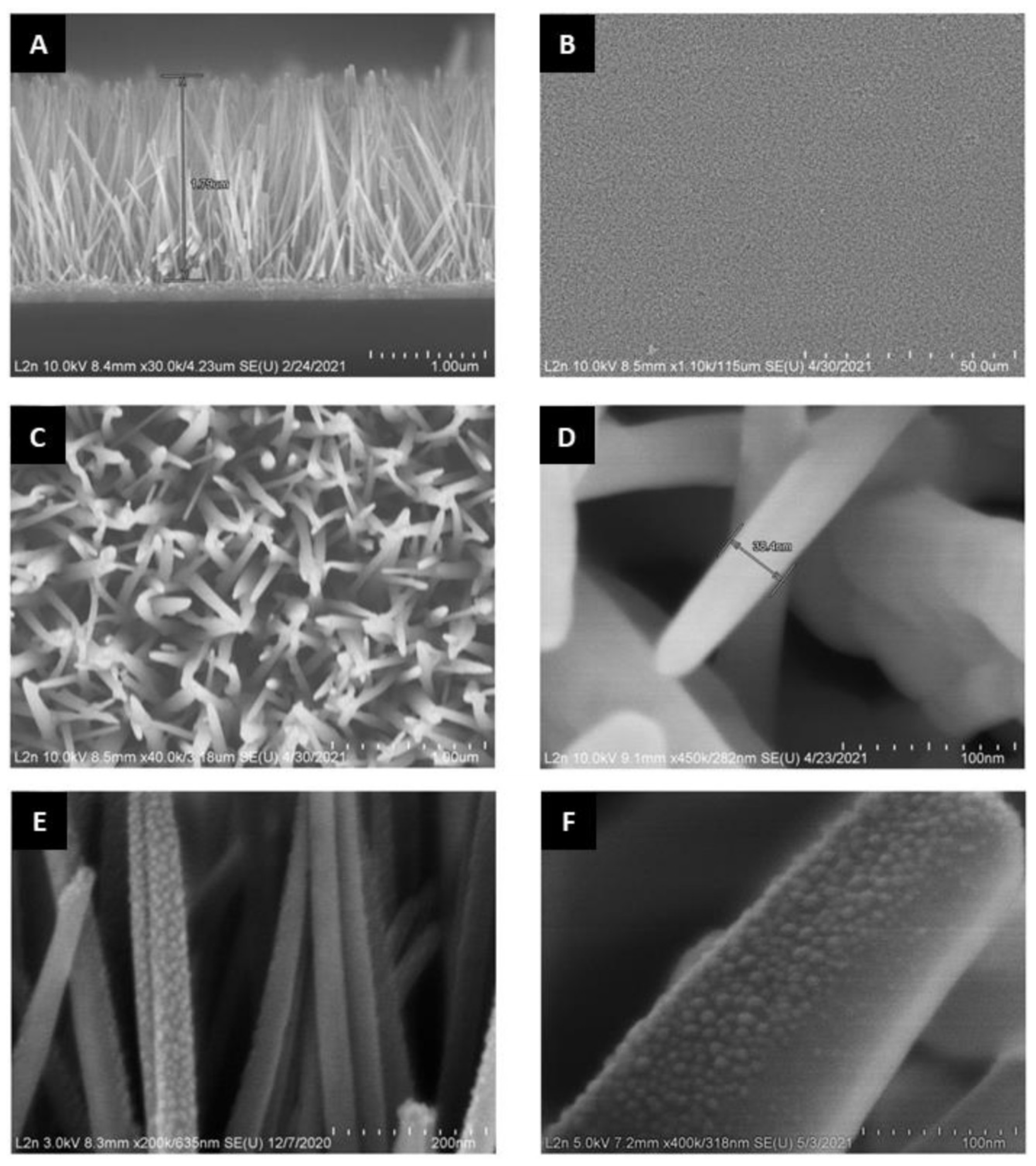
2.1. Preparation of the ZnO Seed Layers
2.2. ZnO Nanowires Synthesis
2.3. Aluminum Nanostructures Fabrication
2.4. Photoluminescence Measurements
2.5. Methylene Blue Photocatalysis Experiments
3. Results and Discussion
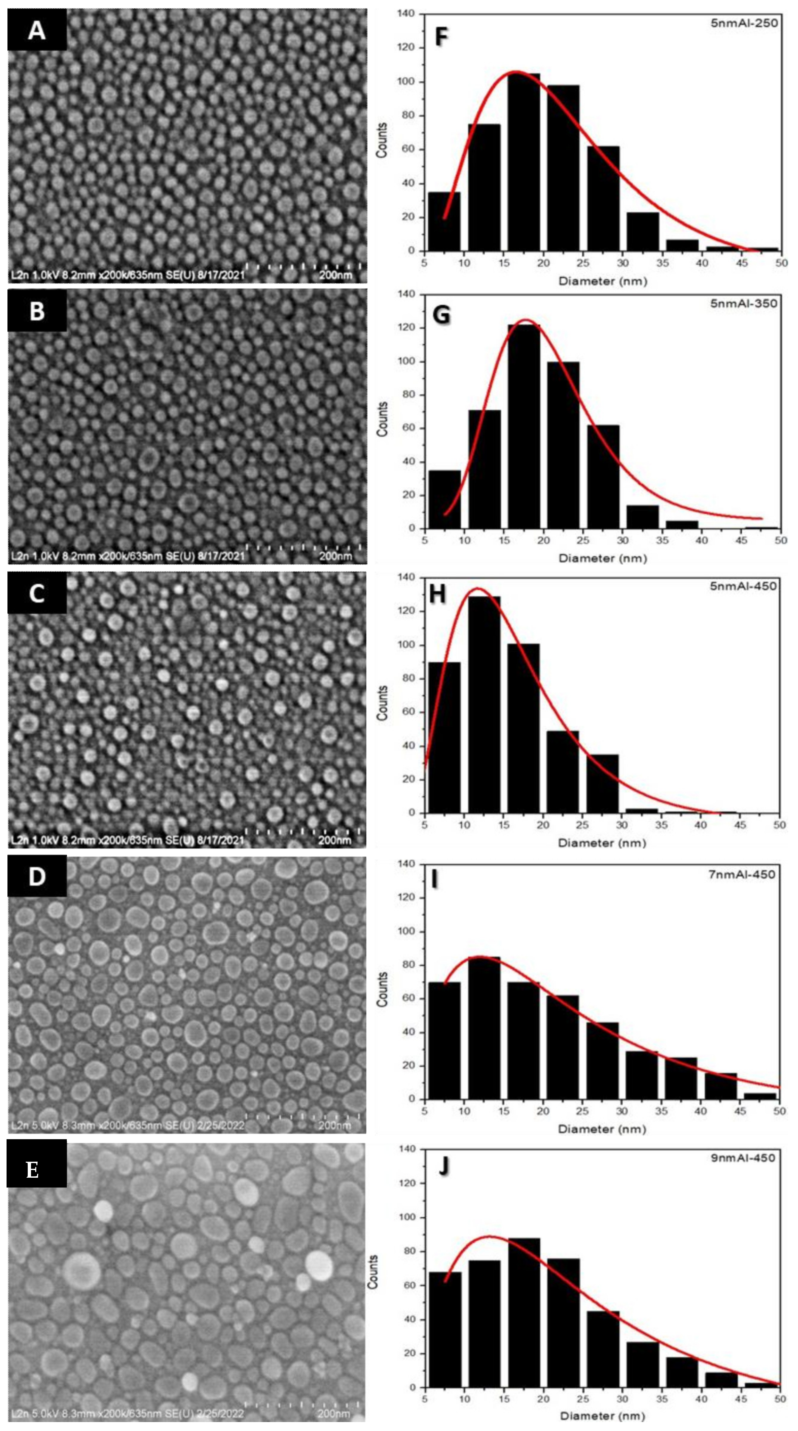
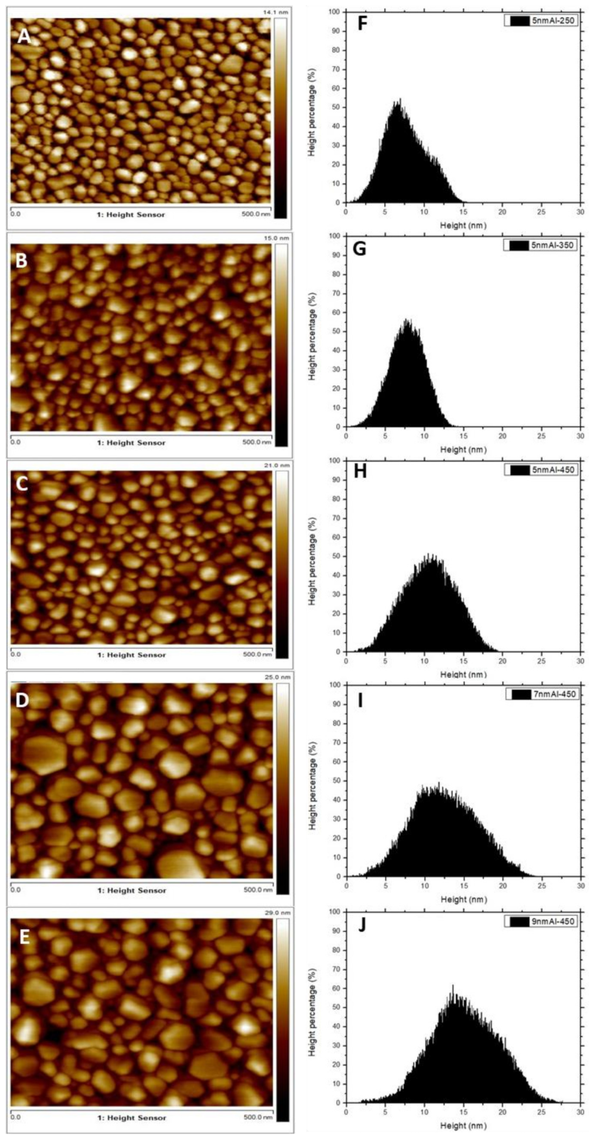
3.1. Parametric Study of the Aluminum Nanostructures Fabrication
3.2. Morphology of ZnONws and ZnONws Covered by the Aluminum Nanostructures
3.3. Optical Properties
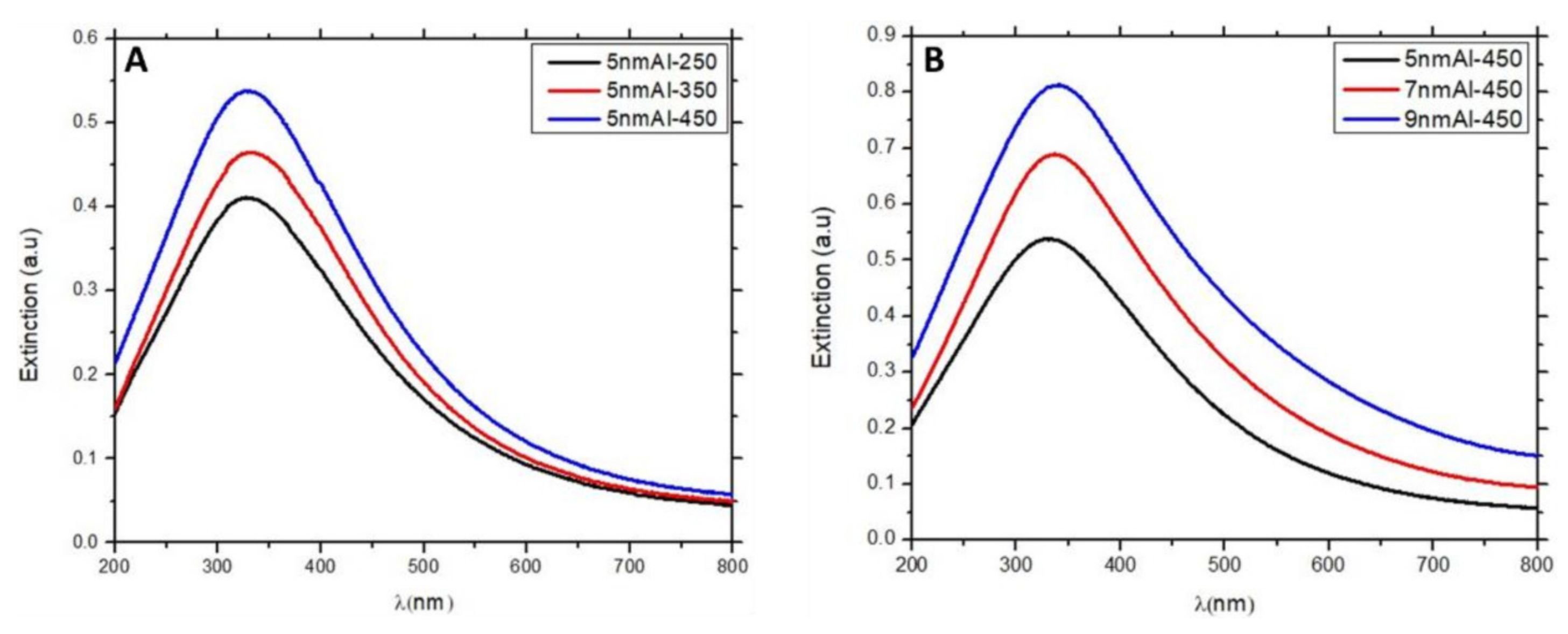
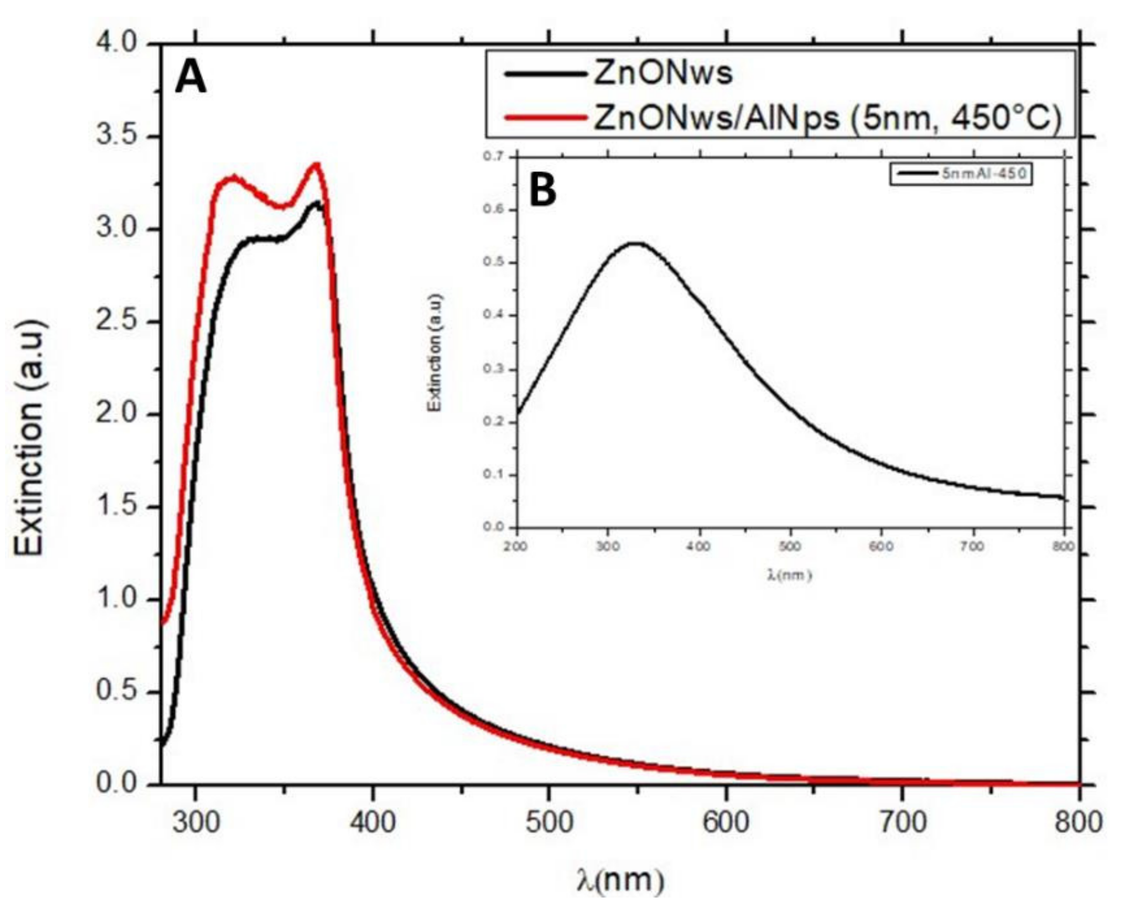
3.3.1. UV-Visible Response
3.3.2. Photoluminescence Response
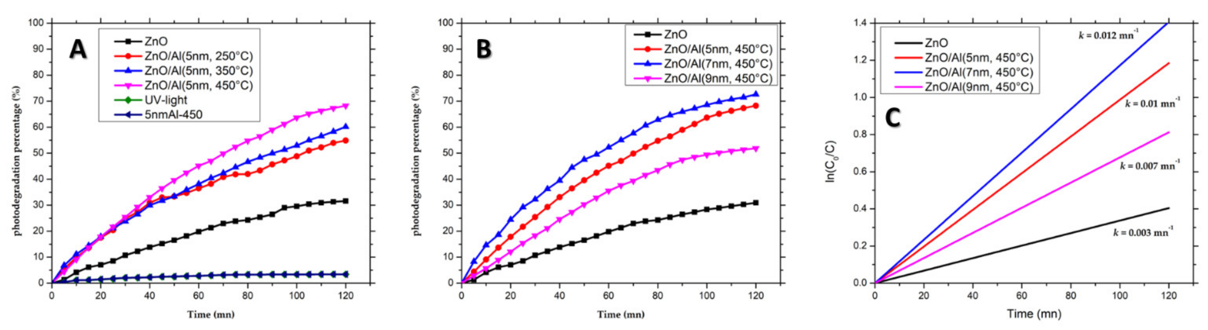
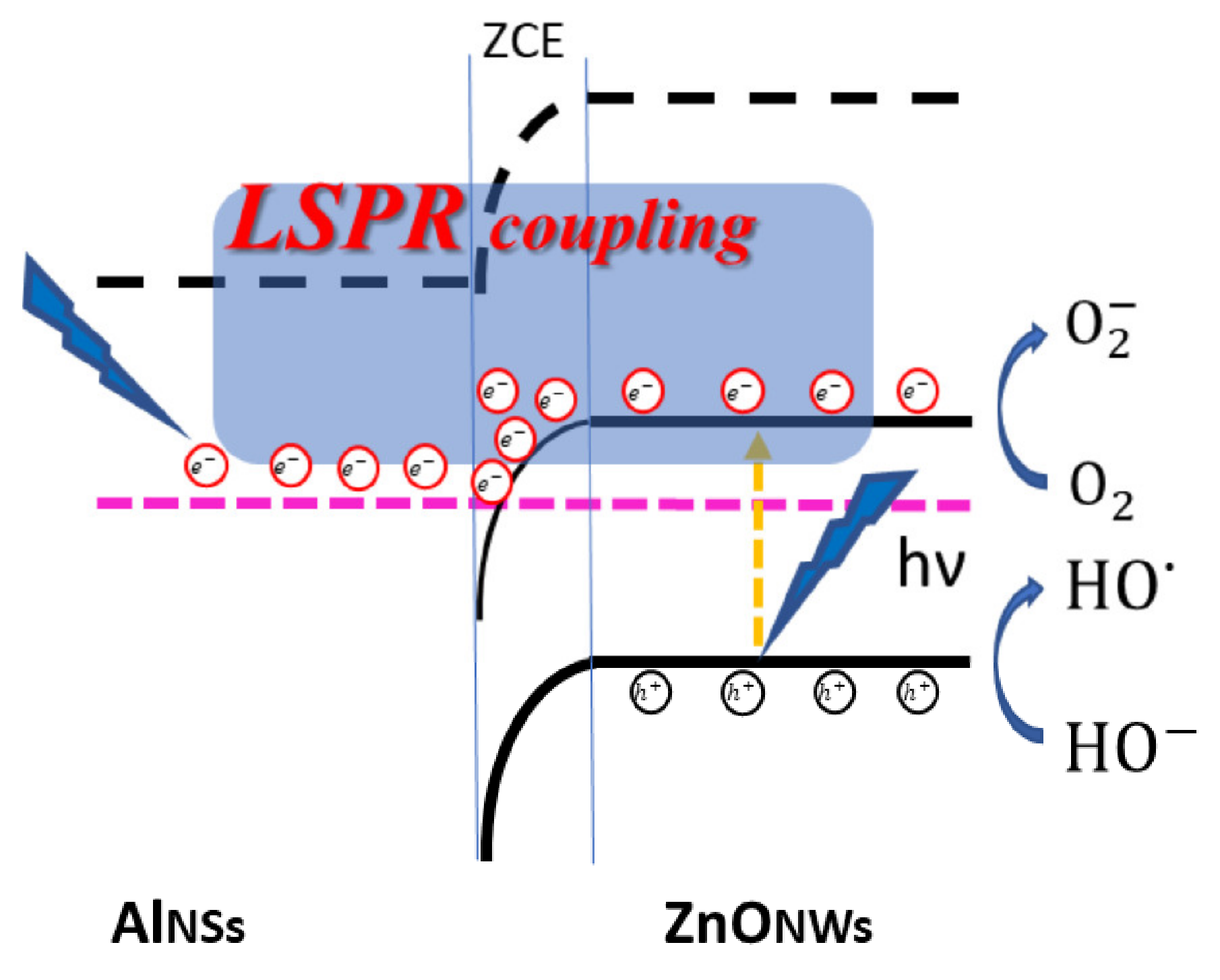
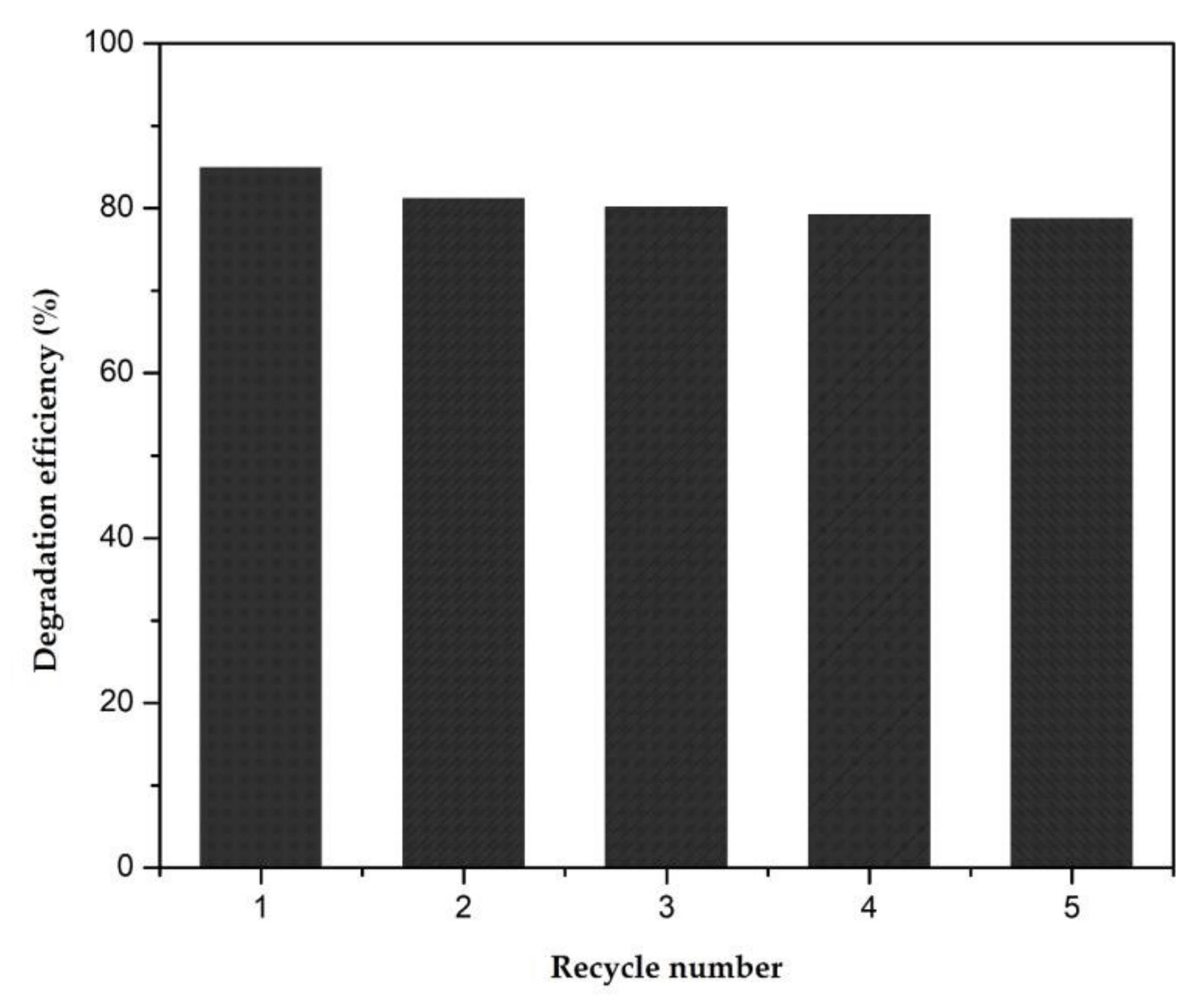
3.4. Photocatalytic Activity in the Presence of Methylene Blue
4. Conclusions
Supplementary Materials
Author Contributions
Funding
Institutional Review Board Statement
Informed Consent Statement
Data Availability Statement
Conflicts of Interest
References
- Samadi, M.; Zirak, M.; Naseri, A.; Kheirabadi, M.; Ebrahimi, M.; Moshfegh, A.Z. Design and Tailoring of One-Dimensional ZnO Nanomaterials for Photocatalytic Degradation of Organic Dyes: A Review. Res. Chem. Intermed. 2019, 45, 2197–2254. [Google Scholar] [CrossRef]
- Laurenti, M.; Cauda, V. Porous Zinc Oxide Thin Films: Synthesis Approaches and Applications. Coatings 2018, 8, 67. [Google Scholar] [CrossRef] [Green Version]
- Triboulet, R. Growth of ZnO Bulk Crystals: A Review. Prog. Cryst. Growth Charact. Mater. 2014, 60, 1–14. [Google Scholar] [CrossRef]
- Shafiei, S.; Nourbakhsh, A.; Ganjipour, B.; Zahedifar, M.; Vakili-Nezhaad, G. Diameter Optimization of VLS-Synthesized ZnO Nanowires, Using Statistical Design of Experiment. Nanotechnology 2007, 18, 355708. [Google Scholar] [CrossRef]
- Chang, P.-C.; Fan, Z.; Wang, D.; Tseng, W.-Y.; Chiou, W.-A.; Hong, J.; Lu, J.G. ZnO Nanowires Synthesized by Vapor Trapping CVD Method. Chem. Mater. 2004, 16, 5133–5137. [Google Scholar] [CrossRef]
- Jarjour, A.; Cox, J.W.; Ruane, W.T.; Wenckstern, H.V.; Grundmann, M.; Brillson, L.J. Single Metal Ohmic and Rectifying Contacts to ZnO Nanowires: A Defect Based Approach. Ann. Phys. 2018, 530, 1700335. [Google Scholar] [CrossRef]
- Obreja, P.; Cristea, D.; Dinescu, A.; Romaniţan, C. Influence of Surface Substrates on the Properties of ZnO Nanowires Synthesized by Hydrothermal Method. Appl. Surf. Sci. 2019, 463, 1117–1123. [Google Scholar] [CrossRef]
- Abdulrahman, A.F.; Ahmed, S.M.; Ahmed, N.M.; Almessiere, M.A. Enhancement of ZnO Nanorods Properties Using Modified Chemical Bath Deposition Method: Effect of Precursor Concentration. Crystals 2020, 10, 386. [Google Scholar] [CrossRef]
- Wang, F.; Zhou, Y.; Pan, X.; Lu, B.; Huang, J.; Ye, Z. Enhanced Photocatalytic Properties of ZnO Nanorods by Electrostatic Self-Assembly with Reduced Graphene Oxide. Phys. Chem. Chem. Phys. 2018, 20, 6959–6969. [Google Scholar] [CrossRef]
- Zhong, Q.; Lan, H.; Zhang, M.; Zhu, H.; Bu, M. Preparation of Heterostructure G-C3N4/ZnO Nanorods for High Photocatalytic Activity on Different Pollutants (MB, RhB, Cr(VI) and Eosin). Ceram. Int. 2020, 46, 12192–12199. [Google Scholar] [CrossRef]
- Kumari, V.; Mittal, A.; Jindal, J.; Yadav, S.; Kumar, N. S-, N- and C-Doped ZnO as Semiconductor Photocatalysts: A Review. Front. Mater. Sci. 2019, 13, 1–22. [Google Scholar] [CrossRef]
- Jasso-Salcedo, A.B.; Palestino, G.; Escobar-Barrios, V.A. Effect of Ag, PH, and Time on the Preparation of Ag-Functionalized Zinc Oxide Nanoagglomerates as Photocatalysts. J. Catal. 2014, 318, 170–178. [Google Scholar] [CrossRef]
- Liu, X.; Zhang, J.; Wang, L.; Yang, T.; Guo, X.; Wu, S.; Wang, S. 3D Hierarchically Porous ZnO Structures and Their Functionalization by Au Nanoparticles for Gas Sensors. J. Mater. Chem. 2011, 21, 349–356. [Google Scholar] [CrossRef]
- Ziashahabi, A.; Prato, M.; Dang, Z.; Poursalehi, R.; Naseri, N. The Effect of Silver Oxidation on the Photocatalytic Activity of Ag/ZnO Hybrid Plasmonic/Metal-Oxide Nanostructures under Visible Light and in the Dark. Sci. Rep. 2019, 9, 11839. [Google Scholar] [CrossRef] [Green Version]
- Agrawal, N.; Zhang, B.; Saha, C.; Kumar, C.; Pu, X.; Kumar, S. Ultra-Sensitive Cholesterol Sensor Using Gold and Zinc-Oxide Nanoparticles Immobilized Core Mismatch MPM/SPS Probe. J. Light. Technol. 2020, 38, 2523–2529. [Google Scholar] [CrossRef]
- Movsesyan, A.; Baudrion, A.-L.; Adam, P.-M. Revealing the Hidden Plasmonic Modes of a Gold Nanocylinder. J. Phys. Chem. C 2018, 122, 23651–23658. [Google Scholar] [CrossRef]
- Chehadi, Z.; Alkees, N.; Bruyant, A.; Toufaily, J.; Girardon, J.-S.; Capron, M.; Dumeignil, F.; Hamieh, T.; Bachelot, R.; Jradi, S. Plasmonic Enhanced Photocatalytic Activity of Semiconductors for the Degradation of Organic Pollutants under Visible Light. Mater. Sci. Semicond. Process. 2016, 42, 81–84. [Google Scholar] [CrossRef]
- Chehadi, Z.; Girardon, J.-S.; Capron, M.; Dumeignil, F.; Jradi, S. Thermoplasmonic-Induced Energy-Efficient Catalytic Oxidation of Glycerol over Gold Supported Catalysts Using Visible Light at Ambient Temperature. Appl. Catal. Gen. 2019, 572, 9–14. [Google Scholar] [CrossRef]
- Kavitha, R.; Kumar, S.G. A Review on Plasmonic Au-ZnO Heterojunction Photocatalysts: Preparation, Modifications and Related Charge Carrier Dynamics. Mater. Sci. Semicond. Process. 2019, 93, 59–91. [Google Scholar] [CrossRef]
- She, P.; Xu, K.; Zeng, S.; He, Q.; Sun, H.; Liu, Z. Investigating the Size Effect of Au Nanospheres on the Photocatalytic Activity of Au-Modified ZnO Nanorods. J. Colloid Interface Sci. 2017, 499, 76–82. [Google Scholar] [CrossRef]
- Knight, M.W.; Liu, L.; Wang, Y.; Brown, L.; Mukherjee, S.; King, N.S.; Everitt, H.O.; Nordlander, P.; Halas, N.J. Aluminum Plasmonic Nanoantennas. Nano Lett. 2012, 12, 6000–6004. [Google Scholar] [CrossRef] [PubMed]
- Muravitskaya, A.; Gokarna, A.; Movsesyan, A.; Kostcheev, S.; Rumyantseva, A.; Couteau, C.; Lerondel, G.; Baudrion, A.-L.; Gaponenko, S.; Adam, P.-M. Refractive Index Mediated Plasmon Hybridization in an Array of Aluminium Nanoparticles. Nanoscale 2020, 12, 6394–6402. [Google Scholar] [CrossRef] [PubMed] [Green Version]
- Liu, S.; Li, M.-Y.; Zhang, J.; Su, D.; Huang, Z.; Kunwar, S.; Lee, J. Self-Assembled Al Nanostructure/ZnO Quantum Dot Heterostructures for High Responsivity and Fast UV Photodetector. Nano-Micro Lett. 2020, 12, 114. [Google Scholar] [CrossRef] [PubMed]
- Liao, Y.-J.; Cheng, C.-W.; Wu, B.-H.; Wang, C.-Y.; Chen, C.-Y.; Gwo, S.; Chen, L.-J. Low Threshold Room-Temperature UV Surface Plasmon Polariton Lasers with ZnO Nanowires on Single-Crystal Aluminum Films with Al 2 O 3 Interlayers. RSC Adv. 2019, 9, 13600–13607. [Google Scholar] [CrossRef] [Green Version]
- Mahdavi, R.; Talesh, S.S.A. Sol-Gel Synthesis, Structural and Enhanced Photocatalytic Performance of Al Doped ZnO Nanoparticles. Adv. Powder Technol. 2017, 28, 1418–1425. [Google Scholar] [CrossRef]
- Baradaran, M.; Ghodsi, F.E.; Bittencourt, C.; Llobet, E. The Role of Al Concentration on Improving the Photocatalytic Performance of Nanostructured ZnO/ZnO:Al/ZnO Multilayer Thin Films. J. Alloys Compd. 2019, 788, 289–301. [Google Scholar] [CrossRef]
- Jia, W.; Shang, Y.; Gong, L.; Chen, X. Synthesis of Al-ZnO Nanocomposite and Its Potential Application in Photocatalysis and Electrochemistry. Inorg. Chem. Commun. 2018, 88, 51–55. [Google Scholar] [CrossRef]
- Peerakiatkhajohn, P.; Butburee, T.; Sul, J.-H.; Thaweesak, S.; Yun, J.-H. Efficient and Rapid Photocatalytic Degradation of Methyl Orange Dye Using Al/ZnO Nanoparticles. Nanomaterials 2021, 11, 1059. [Google Scholar] [CrossRef]
- Noreen, S.; Zafar, S.; Bibi, I.; Amami, M.; Raza, M.A.S.; Alshammari, F.H.; Elqahtani, Z.M.; Basha, B.I.; Alwadai, N.; Nazir, A.; et al. ZnO, Al/ZnO and W/Ag/ZnO Nanocomposite and Their Comparative Photocatalytic and Adsorptive Removal for Turquoise Blue Dye. Ceram. Int. 2022, 48, 12170–12183. [Google Scholar] [CrossRef]
- Messaoudi, O.; Makhlouf, H.; Souissi, A.; Ben assaker, I.; Amiri, G.; Bardaoui, A.; Oueslati, M.; Bechelany, M.; Chtourou, R. Synthesis and Characterization of ZnO/Cu2O Core–Shell Nanowires Grown by Two-Step Electrodeposition Method. Appl. Surf. Sci. 2015, 343, 148–152. [Google Scholar] [CrossRef]
- Syrrokostas, G.; Govatsi, K.; Yannopoulos, S.N. High-Quality, Reproducible ZnO Nanowire Arrays Obtained by a Multiparameter Optimization of Chemical Bath Deposition Growth. Cryst. Growth Des. 2016, 16, 2140–2150. [Google Scholar] [CrossRef]
- Lachebi, I.; Fedala, A.; Djenizian, T.; Hadjersi, T.; Kechouane, M. Morphological and Optical Properties of Aluminum Nanoparticles Deposited by Thermal Evaporation on Heated Substrates. Surf. Coat. Technol. 2018, 343, 160–165. [Google Scholar] [CrossRef]
- Zayats, A.V.; Smolyaninov, I.I.; Maradudin, A.A. Nano-Optics of Surface Plasmon Polaritons. Phys. Rep. 2005, 408, 131–314. [Google Scholar] [CrossRef]
- Dixit, T.; Palani, I.A.; Singh, V. Role of Surface Plasmon Decay Mediated Hot Carriers toward the Photoluminescence Tuning of Metal-Coated ZnO Nanorods. J. Phys. Chem. C 2017, 121, 3540–3548. [Google Scholar] [CrossRef]
- Dixit, T.; Palani, I.A.; Singh, V. Selective Tuning of Enhancement in near Band Edge Emission in Hydrothermally Grown ZnO Nanorods Coated with Gold. J. Lumin. 2016, 170, 180–186. [Google Scholar] [CrossRef]
- Galdámez-Martinez, A.; Santana, G.; Güell, F.; Martínez-Alanis, P.R.; Dutt, A. Photoluminescence of ZnO Nanowires: A Review. Nanomaterials 2020, 10, 857. [Google Scholar] [CrossRef] [PubMed]
- Ghanbari Shohany, B.; Khorsand Zak, A. Doped ZnO Nanostructures with Selected Elements - Structural, Morphology and Optical Properties: A Review. Ceram. Int. 2020, 46, 5507–5520. [Google Scholar] [CrossRef]
- Özgür, Ü.; Alivov, Y.I.; Liu, C.; Teke, A.; Reshchikov, M.A.; Doğan, S.; Avrutin, V.; Cho, S.-J.; Morkoç, H. A Comprehensive Review of ZnO Materials and Related Devices. J. Appl. Phys. 2005, 98, 041301. [Google Scholar] [CrossRef] [Green Version]
- Fonoberov, V.A.; Alim, K.A.; Balandin, A.A.; Xiu, F.; Liu, J. Photoluminescence Investigation of the Carrier Recombination Processes in ZnO Quantum Dots and Nanocrystals. Phys. Rev. B 2006, 73, 165317. [Google Scholar] [CrossRef] [Green Version]
- Movsesyan, A.; Santiago, E.Y.; Burger, S.; Correa-Duarte, M.A.; Besteiro, L.V.; Wang, Z.; Govorov, A.O. Plasmonic Nanocrystals with Complex Shapes for Photocatalysis and Growth: Contrasting Anisotropic Hot-Electron Generation with the Photothermal Effect. Adv. Opt. Mater. 2022, 10, 2102663. [Google Scholar] [CrossRef]
- Negrín-Montecelo, Y.; Movsesyan, A.; Gao, J.; Burger, S.; Wang, Z.M.; Nlate, S.; Pouget, E.; Oda, R.; Comesaña-Hermo, M.; Govorov, A.O.; et al. Chiral Generation of Hot Carriers for Polarization-Sensitive Plasmonic Photocatalysis. J. Am. Chem. Soc. 2022, 144, 1663–1671. [Google Scholar] [CrossRef] [PubMed]
- Rej, S.; Mascaretti, L.; Santiago, E.Y.; Tomanec, O.; Kment, Š.; Wang, Z.; Zbořil, R.; Fornasiero, P.; Govorov, A.O.; Naldoni, A. Determining Plasmonic Hot Electrons and Photothermal Effects during H2 Evolution with TiN–Pt Nanohybrids. ACS Catal. 2020, 10, 5261–5271. [Google Scholar] [CrossRef]
- Bahramian, R.; Moshaii, A.; Eshghi, H. Effect of Seeding Modification of Substrate on the Growth and UV Detection Properties of ZnO Nanowires. Materials Letters 2016, 179, 222–225. [Google Scholar] [CrossRef]
- Yoon, Y.-C.; Park, K.-S.; Kim, S.-D. Effects of Low Preheating Temperature for ZnO Seed Layer Deposited by Sol– Gel Spin Coating on the Structural Properties of Hydrothermal ZnO Nanorods. Thin Solid Films 2015, 597, 125–130. [Google Scholar] [CrossRef]
- Ku, C.-H.; Wu, J.-J. Chemical Bath Deposition of ZnO Nanowire–Nanoparticle Composite Electrodes for Use in Dye-Sensitized Solar Cells. Nanotechnology 2007, 18, 505706. [Google Scholar] [CrossRef]
- Saravanakkumar, D.; Sivaranjani, S.; Kaviyarasu, K.; Ayeshamariam, A.; Ravikumar, B.; Pandiarajan, S.; Veeralakshmi, C.; Jayachandran, M.; Maaza, M. Synthesis and Characterization of ZnO–CuO Nanocomposites Powder by Modified Perfume Spray Pyrolysis Method and Its Antimicrobial Investigation. J. Semicond. 2018, 39, 033001. [Google Scholar] [CrossRef]
- Mittal, M.; Sharma, M.; Pandey, O.P. UV–Visible Light Induced Photocatalytic Studies of Cu Doped ZnO Nanoparticles Prepared by Co-Precipitation Method. Solar Energy 2014, 110, 386–397. [Google Scholar] [CrossRef]


| Average Size (nm) | Average Height (nm) | Shape Factor | |
|---|---|---|---|
| 5 nmAl−250 | 17 | 6.5 | 2.6 |
| 5 nmAl−350 | 17.5 | 7.5 | 2.3 |
| 5 nmAl−450 | 11.5 | 10.5 | 1.1 |
| 7 nmAl−450 | 12 | 13 | 0.9 |
| 9 nmAl−450 | 13.5 | 14.5 | 0.9 |
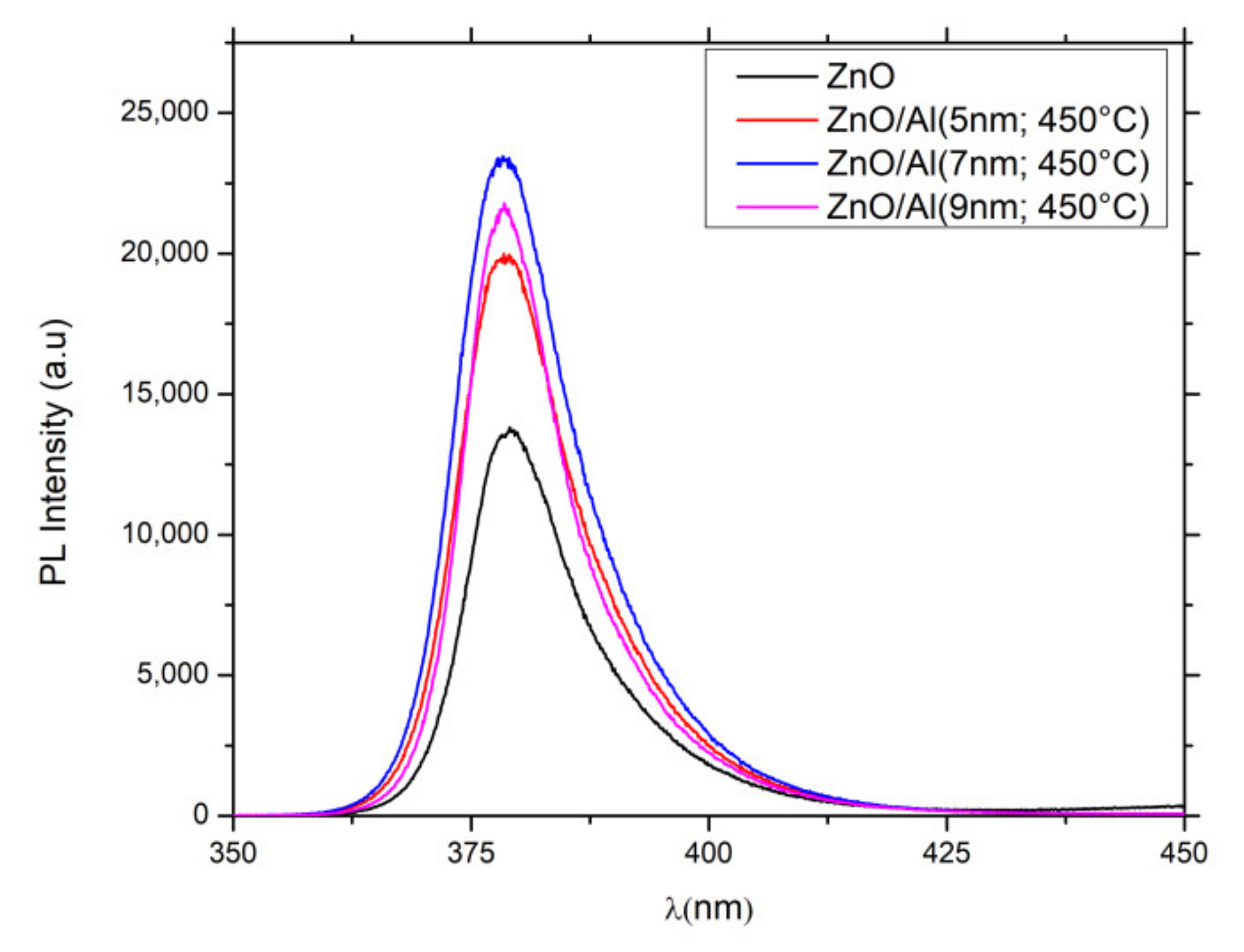
| Centre (nm) | (a.u) | PL Enhancement Factor | |
|---|---|---|---|
| ZnONws | 379.2 | 13,704 | 1 |
| ZnONws/AlNSs (5 nm) | 378.5 | 19,821 | 1.45 |
| ZnONws/AlNSs (7 nm) | 378.5 | 23,190 | 1.70 |
| ZnONws/AlNSs (9 nm) | 378.5 | 21,500 | 1.57 |
Publisher’s Note: MDPI stays neutral with regard to jurisdictional claims in published maps and institutional affiliations. |
© 2022 by the authors. Licensee MDPI, Basel, Switzerland. This article is an open access article distributed under the terms and conditions of the Creative Commons Attribution (CC BY) license (https://creativecommons.org/licenses/by/4.0/).
Share and Cite
Rtimi, M.; Beydoun, N.; Movsesyan, A.; Akil, S.; Kostcheev, S.; Gassmann, X.; Lajnef, M.; Chtourou, R.; Jradi, S. Enhanced Photocatalytic Activity and Photoluminescence of ZnO Nano-Wires Coupled with Aluminum Nanostructures. Nanomaterials 2022, 12, 1941. https://doi.org/10.3390/nano12111941
Rtimi M, Beydoun N, Movsesyan A, Akil S, Kostcheev S, Gassmann X, Lajnef M, Chtourou R, Jradi S. Enhanced Photocatalytic Activity and Photoluminescence of ZnO Nano-Wires Coupled with Aluminum Nanostructures. Nanomaterials. 2022; 12(11):1941. https://doi.org/10.3390/nano12111941
Chicago/Turabian StyleRtimi, Mondher, Nour Beydoun, Artur Movsesyan, Suzanna Akil, Sergei Kostcheev, Xavier Gassmann, Mohamed Lajnef, Radhouane Chtourou, and Safi Jradi. 2022. "Enhanced Photocatalytic Activity and Photoluminescence of ZnO Nano-Wires Coupled with Aluminum Nanostructures" Nanomaterials 12, no. 11: 1941. https://doi.org/10.3390/nano12111941
APA StyleRtimi, M., Beydoun, N., Movsesyan, A., Akil, S., Kostcheev, S., Gassmann, X., Lajnef, M., Chtourou, R., & Jradi, S. (2022). Enhanced Photocatalytic Activity and Photoluminescence of ZnO Nano-Wires Coupled with Aluminum Nanostructures. Nanomaterials, 12(11), 1941. https://doi.org/10.3390/nano12111941