Article

Broadband Optical Constants and Nonlinear Properties of SnS2 and SnSe2

by
Georgy A. Ermolaev
1,
Dmitry I. Yakubovsky
1,
Marwa A. El-Sayed
1,2,
Mikhail K. Tatmyshevskiy
1,
Arslan B. Mazitov
1,3,
Anna A. Popkova
4,
Ilya M. Antropov
4,
Vladimir O. Bessonov
4,
Aleksandr S. Slavich
1,
Gleb I. Tselikov
1,
Ivan A. Kruglov
1,3,
Sergey M. Novikov
1,
Andrey A. Vyshnevyy
1,
Andrey A. Fedyanin
4,
Aleksey V. Arsenin
1 and
Valentyn S. Volkov
1,*
1
Center for Photonics and 2D Materials, Moscow Institute of Physics and Technology, 9 Institutsky Lane, 141700 Dolgoprudny, Russia
2
Department of Physics, Faculty of Science, Menoufia University, Shebin El-Koom 32511, Egypt
3
Dukhov Research Institute of Automatics (VNIIA), 22 Suschevskaya St., 127055 Moscow, Russia
4
Faculty of Physics, Lomonosov Moscow State University, 119991 Moscow, Russia
*
Author to whom correspondence should be addressed.
Nanomaterials 2022, 12(1), 141; https://doi.org/10.3390/nano12010141
Submission received: 5 December 2021 / Revised: 24 December 2021 / Accepted: 28 December 2021 / Published: 31 December 2021

Abstract

:
SnS2 and SnSe2 have recently been shown to have a wide range of applications in photonic and optoelectronic devices. However, because of incomplete knowledge about their optical characteristics, the use of SnS2 and SnSe2 in optical engineering remains challenging. Here, we addressed this problem by establishing SnS2 and SnSe2 linear and nonlinear optical properties in the broad (300–3300 nm) spectral range. Coupled with the first-principle calculations, our experimental study unveiled the full dielectric tensor of SnS2 and SnSe2. Furthermore, we established that SnS2 is a promising material for visible high refractive index nanophotonics. Meanwhile, SnSe2 demonstrates a stronger nonlinear response compared with SnS2. Our results create a solid ground for current and next-generation SnS2- and SnSe2-based devices.

1. Introduction

Van der Waals materials have emerged as a promising building block for next-generation optical and electronic devices [1,2,3,4,5,6,7,8]. Their planar structure [9,10] and the outstanding compatibility with existing manufacturing techniques [11,12,13,14,15] make such materials ideal for integration into modern industrial and scientific devices. Among layered materials, graphene [16], MoS2 [17], and hBN [18] have received the most attention, as they were the first [19,20,21] to catch researchers’ interest during the “two-dimensional” revolution [22] in material science. However, the number of known layered materials has increased exponentially over the last decade, with more than 1000 layered compounds being isolated and identified [23]. As a result, their properties are largely unexplored, which considerably impedes their application. In particular, the optical properties of tin-based dichalcogenides SnS2 and SnSe2 [24,25] are mostly unknown, with rare reports [26,27,28,29,30] on their absorption properties. Nonetheless, SnS2 and SnSe2 have already demonstrated their huge potential in optoelectronic applications, such as field-effect transistors [31,32,33], solar cells [34,35], saturable absorbers [36,37,38], photonic crystals [39,40], and photodetectors [41,42]. Hence, broadband linear and nonlinear optical properties are highly desired for the acceleration of the development of SnS2 and SnSe2-based devices.
Here, the objective of the present work is the comprehensive optical characterization of SnS2 and SnSe2. Using spectroscopic ellipsometry and first-principle calculations, we determine the full broadband dielectric tensor of SnS2 and SnSe2 from ultraviolet to mid-infrared wavelengths (300–3300 nm). The results demonstrate a high dielectric response (n > 3) with zero losses in a wide spectral range: 560–3300 nm for SnS2 and 1300–3300 nm for SnSe2. Moreover, we measured the second-order nonlinear optical susceptibility of SnS2 and SnSe2 at wavelengths ranging from 750 to 1050 nm. Finally, our results revealed that SnS2 is a high refractive index material, which fills the important gap in the visible spectrum between bandgap energies of GaP and TiO2, which makes SnS2 a promising material for all-dielectric nanophotonics.

2. Results and Discussion

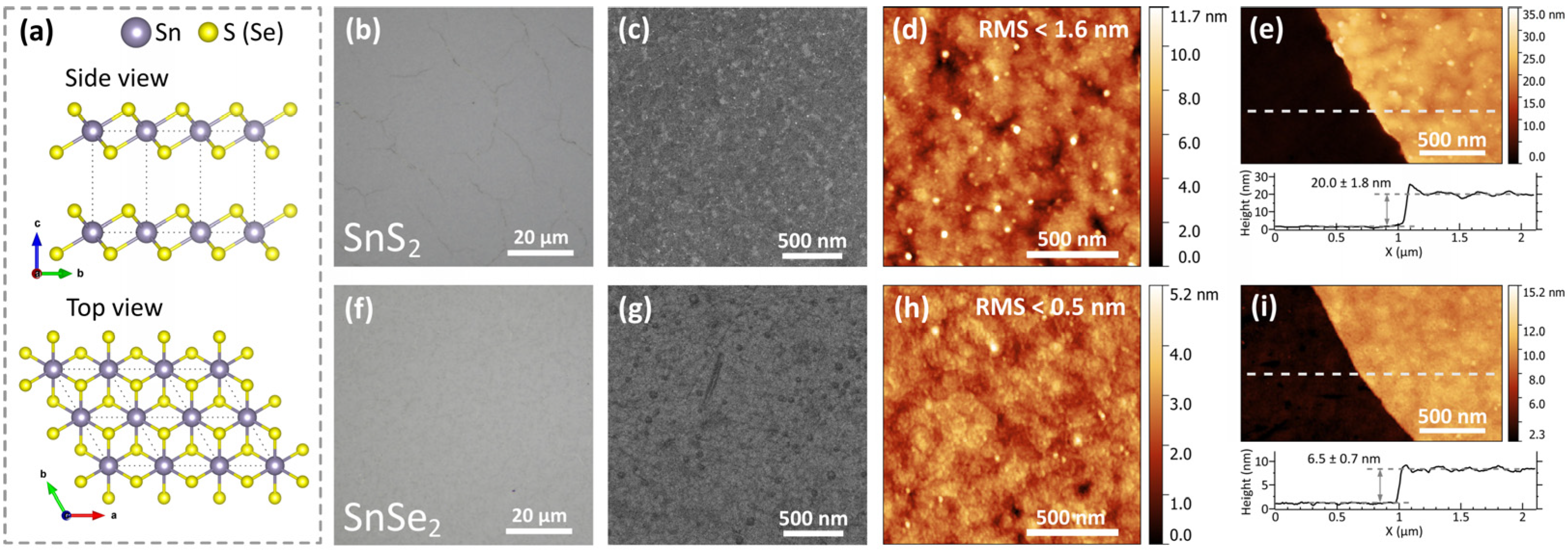
2.1. Surface and Structural Morphology Study

Thin films of SnS2 and SnSe2 were synthesized by the chemical vapor deposition (CVD) method and transferred on a quartz substrate. Figure 1a schematically illustrates the crystal structure of 1T-SnS2 or SnSe2 viewed along c- axis and the a-axis. This crystal configuration is the most common atoms’ arrangement for SnS2 and SnSe2, where layers stack directly above one another [43,44]. Optical microscopy photographs in Figure 1b,f show the uniform substrate’s coverage of synthesized SnS2 and SnSe2 films. Likewise, scanning electron microscopy (SEM) images in Figure 1c,g confirm the films’ full-area coverage and homogeneity at the microscale. In addition, we checked the films’ surface by atomic force microscopy (AFM), demonstrating an atomically smooth surface with root mean square (RMS) roughness of less than 1.6 nm and 0.5 nm for SnS2 and SnSe2, respectively. Ultimately, we accurately measured the films’ thickness via AFM topographical scans (Figure 1e,i). They yielded 20.0 ± 1.8 nm and 6.5 ± 0.7 nm thicknesses for SnS2 and SnSe2 films, correspondingly.

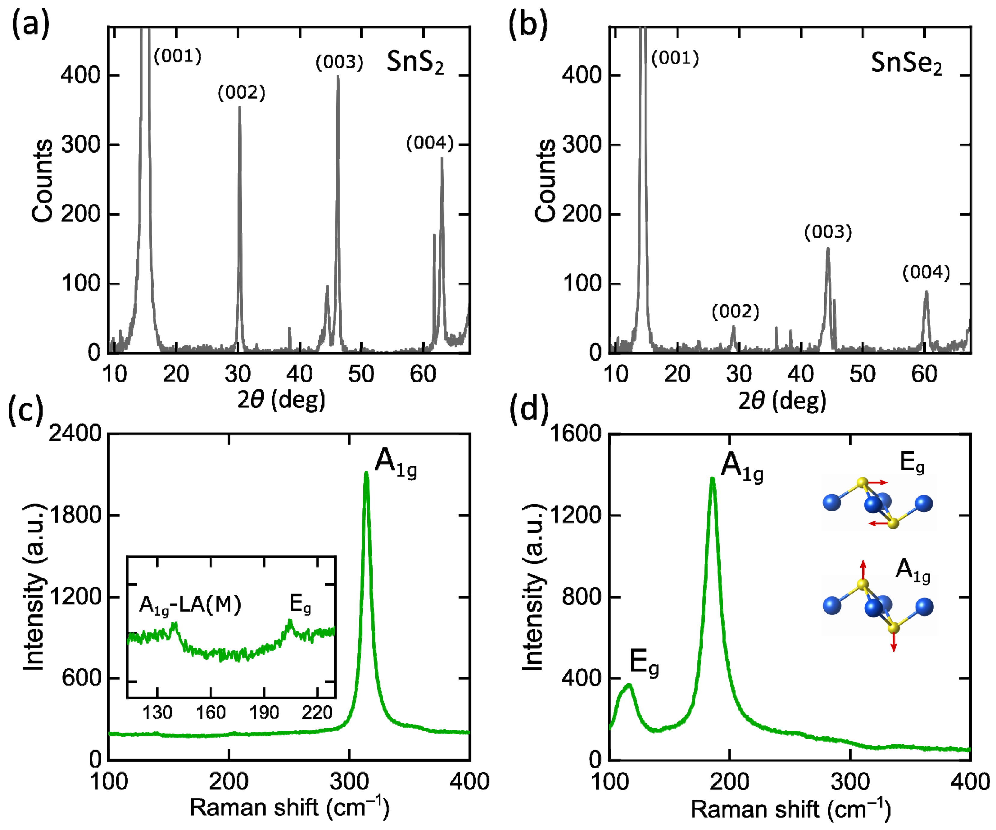
2.2. Analysis of the Crystal Structure and Raman Characterization

In nature, SnS2 and SnSe2 exist in several phase modifications [45,46], including 1T, 2H, 4H, and 18R polytypes. To identify the phase of our samples, we performed X-ray diffraction (XRD), whose spectra are displayed in Figure 2a,b. According to the Joint Committee on Powder Diffraction Standards (card No. 23-0677 and 89-2939) and previous publications [27,47,48], the obtained XRD patterns reveal the hexagonal lattice configuration, which could be 1T or 2H, for SnS2 and SnSe2 with lattice parameters a = b = 3.6486 Å and c = 5.8992 Å for SnS2 and a = b = 3.811 Å and c = 6.137 Å for SnSe2.
Aside from XRD characterization, we utilized Raman spectroscopy at 532 nm excitation wavelength (Figure 2c,d) to distinguish between two hexagonal configurations, 1T and 2H. Raman spectrum of SnS2 reveals out-of-plane vibration mode A1g at ~314 cm−1 and in-plane vibration of Eg at ~205 cm−1, corresponding to 1T polytype [44,49,50]. Similar to SnS2, SnSe2 Raman spectrum has two characteristic phonon modes: A1g mode at ~185 cm−1 and Eg mode at ~116.5 cm−1, associated with 1T-phase [36,51]. Moreover, Raman spectra at numerous locations of our samples demonstrate the same A1g and Eg peak positions, additionally validating the homogeneity of the studied SnS2 and SnSe2 thin films.

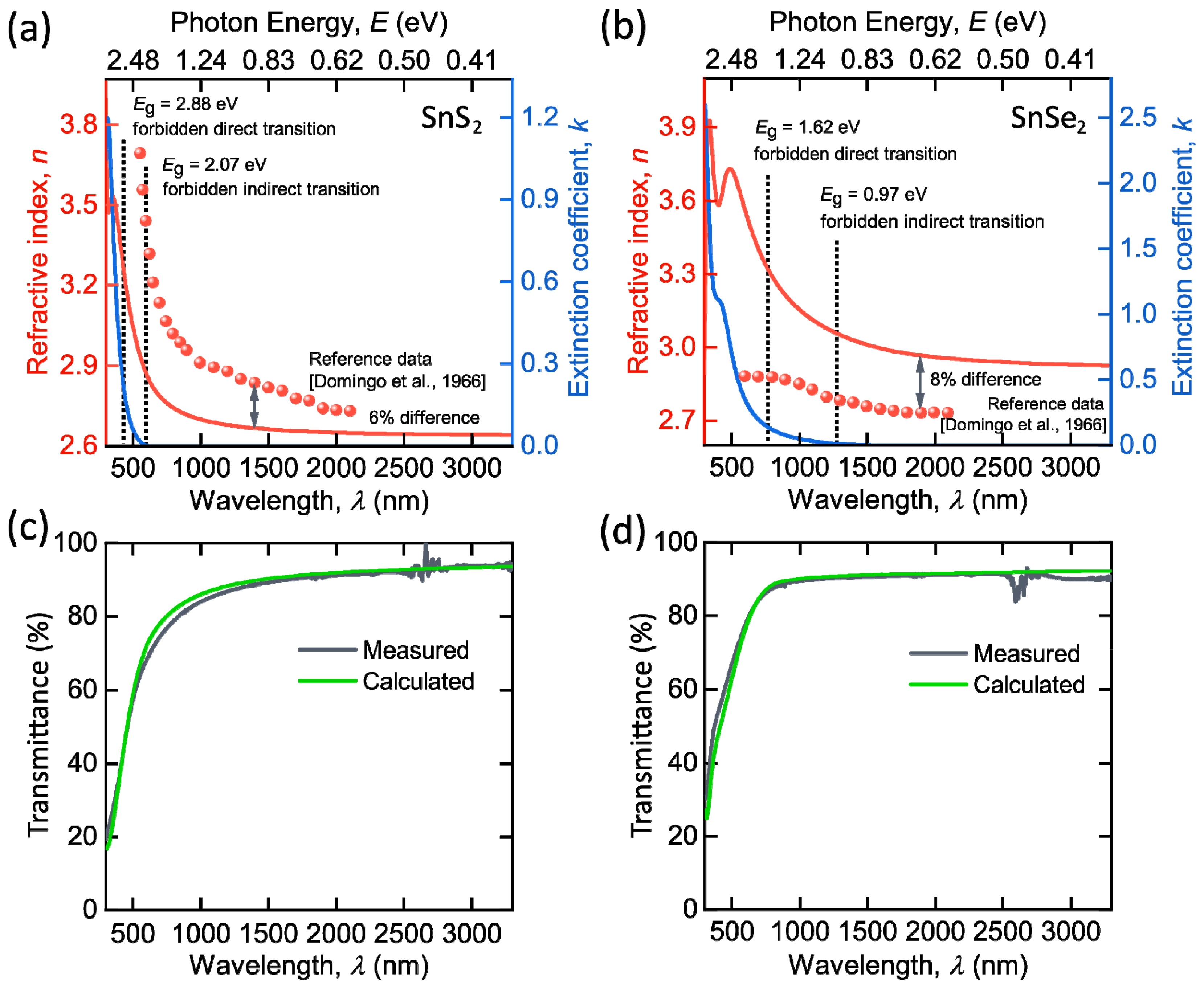
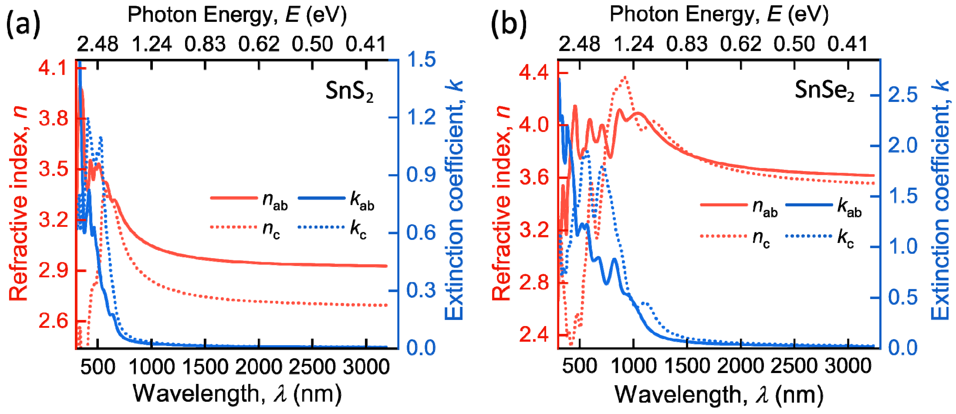
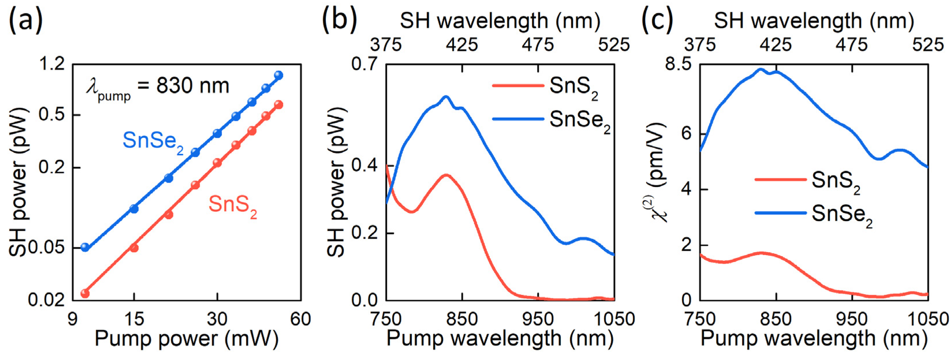
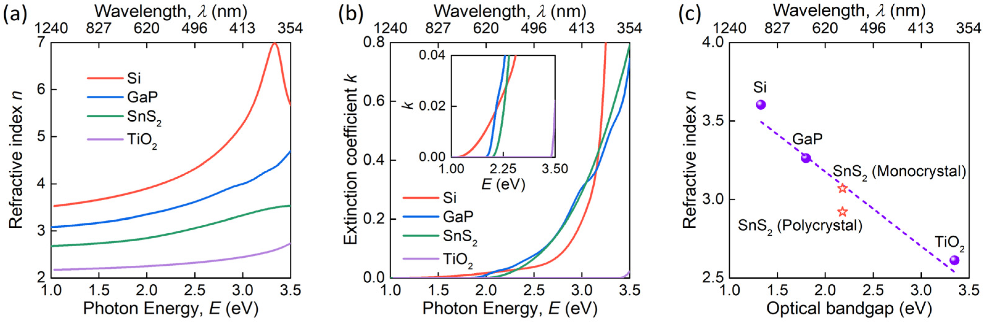
2.3. Optical Properties of SnS2 and SnSe2 Films

We investigated broadband optical constants of SnS2 and SnSe2 films through spectroscopic ellipsometry. We employed a two-layer optical model for ellipsometry data analysis: quartz substrate with SnS2 or SnSe2 film with the thickness determined from AFM (Figure 3e,i). Similar to other TMDCs [52,53], we describe SnS2 and SnSe2 dielectric function by the Tauc–Lorentz oscillator model (see Methods) [54,55]. Figure 3a,b shows the resulting optical constants n and k for SnS2 and SnSe2 films. Interestingly, we did not observe excitons for SnS2 and SnSe2, which can be explained by their indirect bandgap, in contrast, to the direct bandgap in MoS2 and WS2 [56,57]. Apart from the dielectric function, Tauc–Lorentz oscillator parameters allow us to obtain the positions of critical points of joint density of states: 3.91 eV (317 nm) for SnS2; 2.87 eV (432 nm) and 3.98 eV (311 nm) for SnSe2. Furthermore, SnS2 and SnSe2 both have zero absorption (k ~ 0) at a broad wavelength range, starting from 560 and 1300 nm (Figure 3a,b), respectively. For reference, we also plotted in Figure 3a,b refractive indices and bandgap transitions of SnS2 and SnSe2, determined by Domingo and coworkers [26]. As expected, the fundamental absorption edge coincides with the forbidden indirect transitions (Figure 3a,b), supporting our results in Figure 3a,b. For additional verification, we also measured the transmittance spectra of our samples (Figure 3c,d) and compared them with the transfer matrix calculations [58], based on optical constants from Figure 3a,b. Evidently, calculated and measured transmittance agree well, thereby validating our n and k in Figure 3a,b.
To retrieve the full dielectric tensor, we leveraged first-principle calculations (Methods). Figure 4 shows the resulting refractive index and extinction coefficient along the ab-plane (nab and kab) and c-axis (nc and kc). The first-principle calculations reproduce the shape of the experimental dielectric function and render the major optical features: a wide zero-absorption spectral range and high dielectric response. However, first-principle calculations overestimate values of dielectric function since the computations were performed assuming the ideal crystalline structure, whereas the studied CVD-grown films have a polycrystalline structure. Nevertheless, first-principle calculations provide access to the full dielectric permittivity tensor, allowing us to estimate the anisotropic optical properties, which are the most noticeable for SnS2 with birefringence Δn = nabnc ≈ 0.3 and almost negligible for SnSe2. In contrast, ellipsometry is nearly insensitive to optical constants along the c-axis, as explained by Ermolaev and colleagues [56,59]. Thus, our computations reveal for the first time the optical anisotropy in SnS2 and SnSe2, which could be relevant in next-generation anisotropic nanophotonics [60].
In the light of the rapid development of nonlinear optical devices based on SnS2 and SnSe2 [36,37,61], we also measured their nonlinear optical response (Figure 5). Specifically, we measured the second harmonic generation (SHG) in transmission geometry using 150 fs laser pulses focused into a 50 µm spot in diameter (see Methods). Figure 5a shows the SHG power dependence with the expected slope of 2 (2.01 ± 0.02 for SnS2 and 2.02 ± 0.04 for SnSe2), confirming the second-order nonlinear process and the absence of saturation effects. SHG spectra of SnS2 and SnSe2 are shown in Figure 5b. For SnSe2, SHG resonance is at 415 nm (2.98 eV), associated with the 2 photon direct transition at the critical point (2.87 eV) found above from ellipsometry measurements. The presence of SH signal at large pump wavelengths indicates the contribution of direct transitions with lower energies, meaning that the direct transition of SnSe2 is less than 2.36 eV. In contrast, for SnS2, the SH signal is negligible at large wavelengths. Therefore, the SHG resonance observed at the SH wavelength of 420 nm (2.95 eV) can be associated with the lowest energy direct transition of SnS2 in agreement with Domingo and colleagues’ work [26].
To calculate the nonlinear optical susceptibility, we implemented the method, described in Boyd’s book [62]. The technique relies on the following equation for the average power of SHG transmitted through sample:
P ( 2 ω ) = 16 2 | χ ( 2 ) | 2 π S P 2 ( ω ) L 2 ϵ 0 r 2 f τ c n ω 2 n 2 ω λ 2 sin c 2 ( Δ k L 2 )
where χ ( 2 ) is a nonlinear optical susceptibility, S = 0.94 is the shape factor for Gaussian pulses, ϵ 0 is the permittivity of vacuum, c is the speed of light, f = 80 MHz is the pulse repetition rate, τ = 150 fs is the pulse duration, r = 25 µm is the focal spot radius, L is a sample thickness, λ is a pump wavelength, Δ k is the wavevectors mismatch of the pump and SH waves, n ω and n 2 ω are refractive indices of material at pump and harmonic wavelengths, and P ( ω ) and P ( 2 ω ) are average power of the pump and the second harmonic radiation, respectively. In our case, the coherence length L c o h = λ / ( 4 n 2 ω 4 n ω ) of the observed processes is several hundred nanometers (from 300 nm to 900 nm for SnS2 and from 450 to 600 nm for SnSe2), which significantly exceeds the thickness of the films (Figure 1e,f). Thus, we can assume that the SHG is phase-matched and, hence, sin c 2 ( Δ k L / 2 ) = 1 . It allows us to evaluate SnS2 and SnSe2 nonlinear optical susceptibility, displayed in Figure 5c.
Finally, we want to underline that SnS2 is a promising material for all-dielectric nanophotonics [63,64], demanding a high refractive index and low absorption. As shown in Figure 6, SnS2 meets both requirements since it possesses a refractive index n ≈ 2.8 and zero extinction in the visible and infrared ranges. More importantly, SnS2 could even compete with classical high refractive index materials such as Si, GaP, and TiO2 [65,66,67,68]. In particular, SnS2 has a wider transparency region compared with GaP and Si and a larger refractive index than TiO2 (Figure 6). More surprisingly, when we use the refractive index from first-principle calculations (Figure 4a) for monocrystalline SnS2, it perfectly fits into the correlation line between the refractive indices and optical bandgaps of high refractive index materials (Figure 6c). Therefore, SnS2 enables the essential spectral range of all-dielectric nanophotonics between GaP and TiO2.

3. Materials and Methods

3.1. Materials

CVD-grown full-area coverage SnS2 and SnSe2 samples of thin films were purchased from 2d Semiconductors Inc. (2d Semiconductors Inc., Scottsdale, AZ, USA). The samples with an area of 1 × 1 cm2 were grown by CVD on sapphire substrates and subsequently transferred on quartz substrates.

3.2. Surface Morphology Characterization

The surface morphology of SnS2 and SnSe2 thin films was analysed by an optical microscope (Nikon LV150, Tokyo, Japan) with a digital camera DS-Fi3, as well as the scanning electron microscope (SEM) using the acceleration voltage of 30 kV and different magnifications (JEOL JSM-7001F, Tokyo, Japan) to prove films homogeneity. The film surface morphology was studied by atomic force microscopy (AFM, notegra, Nt-MDT Spectrum Instruments, Moscow, Russia) in semi-contact mode using a silicon tip with a radius <10 nm and resonance frequency of ~250 kHz (HA_NC Etalon, Tipsnano, Tallinn, Estonia) to determine surface roughnesses and films thicknesses.

3.3. Crystal Structure Characterization

X-ray diffraction (XRD) characterization was performed by X-ray diffractometer (ARL X’TRA, Thermo Fisher Scientific, Waltham, MA, USA) using Cu Kα1 radiation line (λ = 1.54 Å) to analyze the crystal structure of the films using a regime of 2θ-scan with angles range of 5°–75° with a step of 0.05° and accumulation time of 2 s.

3.4. Raman Characterization

The Raman spectra were measured with a confocal scanning Raman microscope Horiba LabRAM HR Evolution (HORIBA Ltd., Kyoto, Japan) with 532 nm linearly polarized excitation laser, 1800 lines/mm diffraction grating, and ×100 objective (N.A. = 0.90) using a spectra range of 100–450 cm−1. The spectra were recorded with 3.5 mW incident laser power, with an integration time of 10 s and 10 spectra accumulation.

3.5. Ellipsometry Analysis

The optical constants n and k of SnS2 and SnSe2 were measured using a variable-angle spectroscopic ellipsometer (VASE, J.A. Woollam Co., Lincoln, NE, USA), working at room temperature, at variable incidence angles 30°–75° with a step of 5° and wide spectral range from 300 to 3300 nm with a step of 1 nm, having the spotlight of size ~1 mm around the center of the sample, utilizing the high precision optical alignment. To fit the measured ellipsometric parameters Ψ and Δ, we used the Tauc–Lorentz oscillator model was used, defined by the following formula:
ε 2 = { 1 E · A E 0 C ( E E g ) 2 ( E 2 E 0 2 ) 2 + C 2 E 2   f o r   E > E g 0                                                           f o r   E < E g ,
where E is the energy of the photon, A is the oscillator strength, C is the oscillator broadening, E g is the optical band-gap, E 0 is the oscillator central energy, and the real part of the dielectric function ε 1 was obtained from the imaginary part ε 2 using the Kramers–Kronig integration, plus ε , to account for high energy electronic transitions. For SnS2, we used one Tauc–Lorentz oscillator with the following parameters: A = 54.613 eV; C = 1.626 eV; E 0 = 3.911 eV; E g = 1.970 eV and ε = 5.031. For SnSe2, we used two Tauc–Lorentz oscillators with the following parameters: A 1 = 14.435 eV; C 1 = 1.345 eV; E 01 = 2.870 eV; A 2 = 20.432 eV; C 2 = 0.875 eV; E 02 = 3.981 eV; E g = 0.736 eV and ε = 4.445.

3.6. Optical Properties Characterization

Optical transmittance spectra of SnS2 and SnSe2 films on quartz were measured with a spectrophotometer (Cary 5000 UV-Vis-NIR, Agilent Tech., Santa Clara, CA, USA) at a wavelength range of 300–3300 nm.
The nonlinear optical properties of the sample were studied by a home-built multiphoton microscope [69], based on femtosecond Ti:sapphire laser (Coherent Chameleon Ultra 2, Santa Clara city, CA, USA) tunable in the spectral range from 680 to 1080 nm. The laser beam (80 MHz repetition rate, 150 fs pulse duration) was directed through the system, consisting of a half-wave plate on a motorized rotation stage and a Glan–Taylor prism, which provided control of the power and polarization of the incident radiation.
Then, the beam was focused on the sample surface with a 10 cm lens into a 50 μm spot. The sample was mounted on a 3-axis motorized stage (SigmaKoki, Tokyo, Japan) with a minimum step of 0.1 μm, which made it possible to accurately align the sample relative to the pump spot. The SH radiation generated by the sample was collected by an objective lens (N.A. = 0.95, 100x, Olympus, Tokyo, Japan) and directed to the detection channel consisting of a tube lens, filter (FGB39 Thorlabs, Newton, NJ, USA) to cut off the pump radiation, monochoromator, and a scientific CCD camera (Andor Clara, Belfast, United Kingdom). The SH signal was normalized over spectral functions of all optical elements in the detection channel including objective lens transmittance and detector sensitivity spectra. SHG spectra were measured at the same pump intensity for all wavelengths. The experimental setup was fully automated and situated in a black box.

3.7. First-Principle Calculations

The optical properties of SnS2 and SnSe2 were calculated using density functional theory (DFT) implemented in the Vienna Ab Initio Simulation Package [70,71]. Core electrons, their interaction with valence electrons, and exchange correlation effects were described within generalized gradient approximation [72] (Perdew–Burke–Ernzerhof functional) and the projector-augmented wave pseudopotentials [73]. The unit cell parameters were a = b = 3.6486 Å and c = 5.8992 Å for SnS2 and a = b = 3.811 Å and c = 6.137 Å for SnSe2. The calculation was performed in two steps: first, the atomic positions of SnS2 and SnSe2 were relaxed in until the interatomic forces were less than 10−3 eV/Å, and a 1-electron basis set was obtained from a standard DFT calculations. Second, the real and imaginary parts of frequency-dependent dielectric function were calculated using the GW approximation [74]. Cutoff energy of the plane waves basis set was set to 600 eV, and the Γ-centered 11 × 11 × 7 k-points mesh was used to sample the first Brillouin zone.

4. Conclusions

In conclusion, we theoretically and experimentally determined the anisotropic optical constants of SnS2 and SnSe2 in a wide spectral range (300–3300 nm). Our findings reveal a strong dielectric response of SnS2 and SnSe2 and their broad range with zero absorption. More importantly, for SnS2, this range includes visible frequencies, which makes SnS2 a novel high refractive index material, which complements the classical high refractive index materials Si, GaP, and TiO2. Additionally, we measured the second-order nonlinear susceptibility of SnS2 and SnSe2. From a broader perspective, our research enables a foundation for advanced optical engineering with SnS2 and SnSe2.

Author Contributions

V.S.V., A.V.A., A.A.F. and A.A.V. suggested and directed the project; G.A.E., D.I.Y., M.A.E.-S., M.K.T., A.A.P., I.M.A., V.O.B., A.S.S., G.I.T. and S.M.N. performed the measurements and analyzed the data; A.B.M. and I.A.K. provided theoretical support; G.A.E., D.I.Y., M.A.E.-S., M.K.T., A.A.V., A.V.A. and V.S.V. interpreted the experimental results; G.A.E., D.I.Y. and M.A.E.-S. wrote the original draft; G.A.E., D.I.Y., A.A.V., A.V.A. and V.S.V. reviewed and edited the paper; G.A.E., D.I.Y. and M.A.E.-S. contributed equally to this work and should be considered the first co-authors. All authors contributed to the discussions and commented on the paper. All authors have read and agreed to the published version of the manuscript.

Funding

We are gratefully acknowledge the financial support from the Ministry of Science and Higher Education of the Russian Federation (Agreement No. 075-15-2021-987). A.A.P., V.O.B. and A.A.F. acknowledge support by Russian Science Foundation (Grant No. 20-12-00371). G.A.E. acknowledges support by the Fellowship of the President of the Russian Federation to young scientists and postgraduates (SP-2627.2021.5). D.I.Y. acknowledges support by the Fellowship of the President of the Russian Federation to young scientists and postgraduates (SP-1194.2021.5).

Institutional Review Board Statement

Not applicable.

Informed Consent Statement

Not applicable.

Data Availability Statement

The data presented in this study are available upon reasonable request from the corresponding author.

Acknowledgments

The authors thank MIPT’s Shared Research Facilities Center for the use of their equipment.

Conflicts of Interest

The authors declare no conflict of interest.

Appendix A

Table A1. Tabulated optical constants for SnS2 and SnSe2 films from Figure 3a,b.
SnS2SnSe2
λ (nm)nknK
3003.89431.04362.88952.5984
3503.53190.84343.85611.3915
4003.38280.36643.58301.1143
4503.18960.15373.68560.9836
5003.04500.05993.72710.7105
5502.94150.01803.65630.4900
6002.86740.00213.56090.3480
6502.81710.00003.47370.2566
7002.78410.00003.40040.1950
7502.76020.00003.33990.1515
8002.74200.00003.28970.1195
8502.72770.00003.24770.0952
9002.71630.00003.21220.0762
12002.67820.00003.07870.0190
15002.66210.00003.01150.0021
18002.65370.00002.97510.0000
21002.64880.00003.64460.0000
24002.64560.00003.60010.0000
27002.64340.00003.56630.0000
30002.64190.00003.54000.0000
33002.64080.00003.51940.0000

References

  1. Mueller, T.; Xia, F.; Avouris, P. Graphene photodetectors for high-speed optical communications. Nat. Photonics 2010, 4, 297–301. [Google Scholar] [CrossRef] [Green Version]
  2. Zhang, K.; Feng, Y.; Wang, F.; Yang, Z.; Wang, J. Two dimensional hexagonal boron nitride (2D-hBN): Synthesis, properties and applications. J. Mater. Chem. C 2017, 5, 11992–12022. [Google Scholar] [CrossRef]
  3. Pi, L.; Li, L.; Liu, K.; Zhang, Q.; Li, H.; Zhai, T. Recent Progress on 2D Noble-Transition-Metal Dichalcogenides. Adv. Funct. Mater. 2019, 29, 1904932. [Google Scholar] [CrossRef]
  4. Yin, Z.; Li, H.; Li, H.; Jiang, L.; Shi, Y.; Sun, Y.; Lu, G.; Zhang, Q.; Chen, X.; Zhang, H. Single-Layer MoS2 Phototransistors. ACS Nano 2011, 6, 74–80. [Google Scholar] [CrossRef] [PubMed] [Green Version]
  5. Mueller, T.; Malic, E. Exciton physics and device application of two-dimensional transition metal dichalcogenide semiconductors. npj 2D Mater. Appl. 2018, 2, 29. [Google Scholar] [CrossRef] [Green Version]
  6. Thakar, K.; Lodha, S. Optoelectronic and photonic devices based on transition metal dichalcogenides. Mater. Res. Express 2020, 7, 014002. [Google Scholar] [CrossRef]
  7. Manzeli, S.; Ovchinnikov, D.; Pasquier, D.; Yazyev, O.; Kis, A. 2D transition metal dichalcogenides. Nat. Rev. Mater. 2017, 2, 17033. [Google Scholar] [CrossRef]
  8. El-Sayed, M.; Ermolaev, G.; Voronin, K.; Romanov, R.; Tselikov, G.; Yakubovsky, D.; Doroshina, N.; Nemtsov, A.; Solovey, V.; Voronov, A.; et al. Optical Constants of Chemical Vapor Deposited Graphene for Photonic Applications. Nanomaterials 2021, 11, 1230. [Google Scholar] [CrossRef]
  9. Geim, A.K.; Grigorieva, I.V. Van der Waals heterostructures. Nature 2013, 499, 419–425. [Google Scholar] [CrossRef] [PubMed]
  10. Novoselov, K.S.; Mishchenko, A.; Carvalho, A.; Neto, A.H.C. 2D materials and van der Waals heterostructures. Science 2016, 353, aac9439. [Google Scholar] [CrossRef] [Green Version]
  11. Verre, R.; Baranov, D.G.; Munkhbat, B.; Cuadra, J.; Käll, M.; Shegai, T. Transition metal dichalcogenide nanodisks as high-index dielectric Mie nanoresonators. Nat. Nanotechnol. 2019, 14, 679–683. [Google Scholar] [CrossRef] [Green Version]
  12. Munkhbat, B.; Yankovich, A.B.; Baranov, D.G.; Verre, R.; Olsson, E.; Shegai, T.O. Transition metal dichalcogenide metamaterials with atomic precision. Nat. Commun. 2020, 11, 4604. [Google Scholar] [CrossRef] [PubMed]
  13. Mupparapu, R.; Steinert, M.; George, A.; Tang, Z.; Turchanin, A.; Pertsch, T.; Staude, I. Facile Resist-Free Nanopatterning of Monolayers of MoS2 by Focused Ion-Beam Milling. Adv. Mater. Interfaces 2020, 7, 2000858. [Google Scholar] [CrossRef]
  14. Castellanos-Gomez, A.; Barkelid, M.; Goossens, A.M.; Calado, V.E.; van der Zant, H.S.J.; Steele, G.A. Laser-Thinning of MoS2: On Demand Generation of a Single-Layer Semiconductor. Nano Lett. 2012, 12, 3187–3192. [Google Scholar] [CrossRef] [Green Version]
  15. Lin, H.; Xu, Z.-Q.; Cao, G.; Zhang, Y.; Zhou, J.; Wang, Z.; Wan, Z.; Liu, Z.; Loh, K.P.; Qiu, C.-W.; et al. Diffraction-limited imaging with monolayer 2D material-based ultrathin flat lenses. Light. Sci. Appl. 2020, 9, 137. [Google Scholar] [CrossRef]
  16. Mohan, V.B.; Lau, K.-T.; Hui, D.; Bhattacharyya, D. Graphene-based materials and their composites: A review on production, applications and product limitations. Compos. Part B Eng. 2018, 142, 200–220. [Google Scholar] [CrossRef]
  17. Castellanos-Gomez, A. Why all the fuss about 2D semiconductors? Nat. Photonics 2016, 10, 202–204. [Google Scholar] [CrossRef] [Green Version]
  18. Caldwell, J.D.; Aharonovich, I.; Cassabois, G.; Edgar, J.H.; Gil, B.; Basov, D.N. Photonics with hexagonal boron nitride. Nat. Rev. Mater. 2019, 4, 552–567. [Google Scholar] [CrossRef]
  19. Novoselov, K.S.; Geim, A.K.; Morozov, S.V.; Jiang, D.; Zhang, Y.; Dubonos, S.V.; Grigorieva, I.V.; Firsov, A.A. Electric field effect in atomically thin carbon films. Science 2004, 306, 666–669. [Google Scholar] [CrossRef] [PubMed] [Green Version]
  20. Mak, K.F.; Lee, C.; Hone, J.; Shan, J.; Heinz, T.F. Atomically Thin MoS2: A New Direct-Gap Semiconductor. Phys. Rev. Lett. 2010, 105, 136805. [Google Scholar] [CrossRef] [Green Version]
  21. Dean, C.R.; Young, A.; Meric, I.; Lee, C.; Wang, L.; Sorgenfrei, S.; Watanabe, K.; Taniguchi, T.; Kim, P.; Shepard, K.L.; et al. Boron nitride substrates for high-quality graphene electronics. Nat. Nanotechnol. 2010, 5, 722–726. [Google Scholar] [CrossRef]
  22. Geim, A.K.; Novoselov, K.S. The rise of graphene. Nat. Mater. 2007, 6, 183–191. [Google Scholar] [CrossRef]
  23. Mounet, N.; Gibertini, M.; Schwaller, P.; Campi, D.; Merkys, A.; Marrazzo, A.; Sohier, T.; Castelli, I.E.; Cepellotti, A.; Pizzi, G.; et al. Two-dimensional materials from high-throughput computational exfoliation of experimentally known compounds. Nat. Nanotechnol. 2018, 13, 246–252. [Google Scholar] [CrossRef] [Green Version]
  24. Huang, Y.; Xu, K.; Wang, Z.; Shifa, T.A.; Wang, Q.; Wang, F.; Jiang, C.; He, J. Designing the shape evolution of SnSe2 nanosheets and their optoelectronic properties. Nanoscale 2015, 7, 17375–17380. [Google Scholar] [CrossRef] [PubMed]
  25. Huang, Y.; Sutter, E.; Sadowski, J.; Cotlet, M.; Monti, O.L.; Racke, D.A.; Neupane, M.R.; Wickramaratne, D.; Lake, R.; Parkinson, B.A.; et al. Tin Disulfide—An Emerging Layered Metal Dichalcogenide Semiconductor: Materials Properties and Device Characteristics. ACS Nano 2014, 8, 10743–10755. [Google Scholar] [CrossRef] [PubMed]
  26. Domingo, G.; Itoga, R.S.; Kannewurf, C.R. Fundamental Optical Absorption in SnS2 and SnSe2. Phys. Rev. (Ser. I) 1966, 143, 536–541. [Google Scholar] [CrossRef]
  27. Burton, L.A.; Whittles, T.J.; Hesp, D.; Linhart, W.M.; Skelton, J.M.; Hou, B.; Webster, R.F.; O’Dowd, G.; Reece, C.; Cherns, D.; et al. Electronic and optical properties of single crystal SnS2: An earth-abundant disulfide photocatalyst. J. Mater. Chem. A 2015, 4, 1312–1318. [Google Scholar] [CrossRef] [Green Version]
  28. Bertrand, Y.; Leveque, G.; Raisin, C.; Levy, F. Optical properties of SnSe2 and SnS2. J. Phys. C Solid State Phys. 1979, 12, 2907–2916. [Google Scholar] [CrossRef]
  29. Bordas, J.; Robertson, J.; Jakobsson, A. Ultraviolet properties and band structure of SnS2, SnSe2, CdI2, PbI2, BiI3 and BiOI crystals. J. Phys. C Solid State Phys. 1978, 11, 2607–2621. [Google Scholar] [CrossRef]
  30. Mandalidis, S.; Kalomiros, J.; Kambas, K.; Anagnostopoulos, A.N. Optical investigation of SnS2 single crystals. J. Mater. Sci. 1996, 31, 5975–5978. [Google Scholar] [CrossRef]
  31. Song, H.S.; Li, S.L.; Gao, L.; Xu, Y.; Ueno, K.; Tang, J.; Cheng, Y.B.; Tsukagoshi, K. High-performance top-gated monolayer SnS2 field-effect transistors and their integrated logic circuits. Nanoscale 2013, 5, 9666–9670. [Google Scholar] [CrossRef] [PubMed]
  32. Su, G.; Hadjiev, V.; Loya, P.E.; Zhang, J.; Lei, S.; Maharjan, S.; Dong, P.; Ajayan, P.M.; Lou, J.; Peng, H. Chemical Vapor Deposition of Thin Crystals of Layered Semiconductor SnS2 for Fast Photodetection Application. Nano Lett. 2014, 15, 506–513. [Google Scholar] [CrossRef] [PubMed]
  33. Su, Y.; Ebrish, M.A.; Olson, E.J.; Koester, S.J. SnSe2 field-effect transistors with high drive current. Appl. Phys. Lett. 2013, 103, 263104. [Google Scholar] [CrossRef]
  34. Tan, F.; Qu, S.; Wu, J.; Liu, K.; Zhou, S.; Wang, Z. Preparation of SnS2 colloidal quantum dots and their application in organic/inorganic hybrid solar cells. Nanoscale Res. Lett. 2011, 6, 298. [Google Scholar] [CrossRef] [PubMed] [Green Version]
  35. Bai, Y.; Zong, X.; Yu, H.; Chen, Z.-G.; Wang, L. Scalable Low-Cost SnS2 Nanosheets as Counter Electrode Building Blocks for Dye-Sensitized Solar Cells. Chem. Eur. J. 2014, 20, 8670–8676. [Google Scholar] [CrossRef]
  36. Biswas, R.; Dandu, M.; Prosad, A.; Das, S.; Menon, S.; Deka, J.; Majumdar, K.; Raghunathan, V. Strong near band-edge excited second-harmonic generation from multilayer 2H Tin diselenide. Sci. Rep. 2021, 11, 15017. [Google Scholar] [CrossRef]
  37. Yang, H.R.; Liu, X.M. Nonlinear optical response and applications of tin disulfide in the near- and mid-infrared. Appl. Phys. Lett. 2017, 110, 171106. [Google Scholar] [CrossRef]
  38. Lu, H.; Wang, Z.; Huang, Z.; Tao, J.; Xiong, H.; Qiu, W.; Guan, H.; Dong, H.; Dong, J.; Zhu, W.; et al. Resonance-assisted light–control–light characteristics of SnS2 on a microfiber knot resonator with fast response. Photonics Res. 2018, 6, 1137–1143. [Google Scholar] [CrossRef]
  39. Müller, M.; Zentel, R.; Maka, T.; Romanov, S.G.; Sotomayor Torres, C.M. Photonic Crystal Films with High Refractive Index Contrast. Adv. Mater. 2000, 12, 1499–1503. [Google Scholar] [CrossRef]
  40. Jin, Y.; Zhu, Y.; Yang, X.; Jiang, H.; Li, C. In situ synthesis of sulfide-coated polystyrene composites for the fabrication of photonic crystals. J. Colloid Interface Sci. 2006, 301, 130–136. [Google Scholar] [CrossRef] [PubMed]
  41. Gao, W.; Zheng, Z.; Li, Y.; Zhao, Y.; Xu, L.; Deng, H.; Li, J. High performance tin diselenide photodetectors dependent on thickness: A vertical graphene sandwiched device and interfacial mechanism. Nanoscale 2019, 11, 13309–13317. [Google Scholar] [CrossRef]
  42. Fan, C.; Liu, Z.; Yuan, S.; Meng, X.; An, X.; Jing, Y.; Sun, C.; Zhang, Y.; Zhang, Z.; Wang, M.; et al. Enhanced Photodetection Performance of Photodetectors Based on Indium-Doped Tin Disulfide Few Layers. ACS Appl. Mater. Interfaces 2021, 13, 35889–35896. [Google Scholar] [CrossRef]
  43. Joseph, A.; Anjitha, C.; Aravind, A.; Aneesh, P. Structural, optical and magnetic properties of SnS2 nanoparticles and photo response characteristics of p-Si/n-SnS2 heterojunction diode. Appl. Surf. Sci. 2020, 528, 146977. [Google Scholar] [CrossRef]
  44. Smith, A.J.; Meek, P.E.; Liang, W.Y. Raman scattering studies of SnS2 and SnSe2. J. Phys. C Solid State Phys. 1977, 10, 1321–1323. [Google Scholar] [CrossRef]
  45. Mitchell, R.S.; Fujiki, Y.; Ishizawa, Y. Structural polytypism of SnS2. Nature 1974, 247, 537–538. [Google Scholar] [CrossRef]
  46. Gonzalez, J.M.; Oleynik, I.I. Layer-dependent properties of SnS2 and SnSe2 two-dimensional materials. Phys. Rev. B 2016, 94, 125443. [Google Scholar] [CrossRef] [Green Version]
  47. Lin, D.-Y.; Hsu, H.-P.; Tsai, C.-F.; Wang, C.-W.; Shih, Y.-T. Temperature Dependent Excitonic Transition Energy and Enhanced Electron-Phonon Coupling in Layered Ternary SnS2-xSex Semiconductors with Fully Tunable Stoichiometry. Molecules 2021, 26, 2184. [Google Scholar] [CrossRef] [PubMed]
  48. Lin, G.; Zheng, T.; Zhan, L.; Lu, J.; Huang, J.; Wang, H.; Zhou, Y.; Zhang, X.; Cai, W. Tunable structure and optical properties of single crystal SnS2 flakes. Appl. Phys. Express 2020, 13, 035504. [Google Scholar] [CrossRef]
  49. Shown, I.; Samireddi, S.; Chang, Y.-C.; Putikam, R.; Chang, P.-H.; Sabbah, A.; Fu, F.-Y.; Chen, W.-F.; Wu, C.-I.; Yu, T.-Y.; et al. Carbon-doped SnS2 nanostructure as a high-efficiency solar fuel catalyst under visible light. Nat. Commun. 2018, 9, 169. [Google Scholar] [CrossRef] [Green Version]
  50. Lee, N.; Lee, G.; Choi, H.; Park, H.; Choi, Y.; Seo, H.; Ju, H.; Kim, S.; Sul, O.; Lee, J.; et al. Layered deposition of SnS2 grown by atomic layer deposition and its transport properties. Nanotechnology 2019, 30, 405707. [Google Scholar] [CrossRef]
  51. Zhang, Y.; Shi, Y.; Wu, M.; Zhang, K.; Man, B.; Liu, M. Synthesis and Surface-Enhanced Raman Scattering of Ultrathin SnSe2 Nanoflakes by Chemical Vapor Deposition. Nanomaterials 2018, 8, 515. [Google Scholar] [CrossRef] [Green Version]
  52. Ermolaev, G.A.; Yakubovsky, D.I.; Stebunov, Y.V.; Arsenin, A.V.; Volkov, V.S. Spectral ellipsometry of monolayer transition metal dichalcogenides: Analysis of excitonic peaks in dispersion. J. Vac. Sci. Technol. B 2020, 38, 014002. [Google Scholar] [CrossRef]
  53. Ermolaev, G.; El-Sayed, M.; Yakubovsky, D.; Voronin, K.; Romanov, R.; Tatmyshevskiy, M.; Doroshina, N.; Nemtsov, A.; Voronov, A.; Novikov, S.; et al. Optical Constants and Structural Properties of Epitaxial MoS2 Monolayers. Nanomaterials 2021, 11, 1411. [Google Scholar] [CrossRef]
  54. Ermolaev, G.A.; Voronin, K.V.; Tatmyshevskiy, M.K.; Mazitov, A.B.; Slavich, A.S.; Yakubovsky, D.I.; Tselin, A.P.; Mironov, M.S.; Romanov, R.I.; Markeev, A.M.; et al. Broadband Optical Properties of Atomically Thin PtS2 and PtSe2. Nanomaterials 2021, 11, 3269. [Google Scholar] [CrossRef]
  55. Jellison, G.E.; Modine, F.A. Parameterization of the optical functions of amorphous materials in the interband region. Appl. Phys. Lett. 1996, 69, 371–373. [Google Scholar] [CrossRef]
  56. Ermolaev, G.A.; Stebunov, Y.V.; Vyshnevyy, A.A.; Tatarkin, D.E.; Yakubovsky, D.I.; Novikov, S.M.; Baranov, D.G.; Shegai, T.; Nikitin, A.Y.; Arsenin, A.V.; et al. Broadband optical properties of monolayer and bulk MoS2. npj 2D Mater. Appl. 2020, 4, 21. [Google Scholar] [CrossRef]
  57. Niu, Y.; Gonzalez-Abad, S.; Frisenda, R.; Marauhn, P.; Drüppel, M.; Gant, P.; Schmidt, R.; Taghavi, N.S.; Barcons, D.; Molina-Mendoza, A.J.; et al. Thickness-Dependent Differential Reflectance Spectra of Monolayer and Few-Layer MoS2, MoSe2, WS2 and WSe2. Nanomaterials 2018, 8, 725. [Google Scholar] [CrossRef] [PubMed] [Green Version]
  58. Passler, N.C.; Paarmann, A. Generalized 4 × 4 matrix formalism for light propagation in anisotropic stratified media: Study of surface phonon polaritons in polar dielectric heterostructures. J. Opt. Soc. Am. B 2017, 34, 2128–2139. [Google Scholar] [CrossRef] [Green Version]
  59. Ermolaev, G.A.; Tsapenko, A.P.; Volkov, V.S.; Anisimov, A.S.; Gladush, Y.G.; Nasibulin, A.G. Express determination of thickness and dielectric function of single-walled carbon nanotube films. Appl. Phys. Lett. 2020, 116, 231103. [Google Scholar] [CrossRef]
  60. Ermolaev, G.A.; Grudinin, D.V.; Stebunov, Y.V.; Voronin, K.V.; Kravets, V.G.; Duan, J.; Mazitov, A.B.; Tselikov, G.I.; Bylinkin, A.; Yakubovsky, D.I.; et al. Giant optical anisotropy in transition metal dichalcogenides for next-generation photonics. Nat. Commun. 2021, 12, 854. [Google Scholar] [CrossRef]
  61. Niu, K.; Chen, Q.; Sun, R.; Man, B.; Zhang, H. Passively Q-switched erbium-doped fiber laser based on SnS2 saturable absorber. Opt. Mater. Express 2017, 7, 3934–3943. [Google Scholar] [CrossRef]
  62. Boyd, R.W. Nonlinear Optics; Elsevier: Amsterdam, The Netherlands, 2003; ISBN 9780121216825. [Google Scholar]
  63. Evlyukhin, A.B.; Novikov, S.M.; Zywietz, U.; Eriksen, R.L.; Reinhardt, C.; Bozhevolnyi, S.I.; Chichkov, B.N. Demonstration of Magnetic Dipole Resonances of Dielectric Nanospheres in the Visible Region. Nano Lett. 2012, 12, 3749–3755. [Google Scholar] [CrossRef]
  64. Baranov, D.G.; Zuev, D.A.; Lepeshov, S.I.; Kotov, O.V.; Krasnok, A.E.; Evlyukhin, A.B.; Chichkov, B.N. All-dielectric nanophotonics: The quest for better materials and fabrication techniques. Optica 2017, 4, 814–825. [Google Scholar] [CrossRef]
  65. Khmelevskaia, D.; Markina, D.I.; Fedorov, V.V.; Ermolaev, G.A.; Arsenin, A.V.; Volkov, V.S.; Goltaev, A.S.; Zadiranov, Y.M.; Tzibizov, I.A.; Pushkarev, A.P.; et al. Directly grown crystalline gallium phosphide on sapphire for nonlinear all-dielectric nanophotonics. Appl. Phys. Lett. 2021, 118, 201101. [Google Scholar] [CrossRef]
  66. Herzinger, C.M.; Johs, B.D.; McGahan, W.A.; Woollam, J.A.; Paulson, W.M. Ellipsometric determination of optical constants for silicon and thermally grown silicon dioxide via a multi-sample, multi-wavelength, multi-angle investigation. J. Appl. Phys. 1998, 83, 3323–3336. [Google Scholar] [CrossRef]
  67. Tiwald, T.E.; Schubert, M. Measurement of rutile TiO2 dielectric tensor from 0.148 to 33 μm using generalized ellipsometry. Opt. Diagn. Methods Inorg. Mater. II 2000, 4103, 19–29. [Google Scholar]
  68. Ermolaev, G.; Kushnir, S.E.; Sapoletova, N.A.; Napolskii, K.S. Titania Photonic Crystals with Precise Photonic Band Gap Position via Anodizing with Voltage versus Optical Path Length Modulation. Nanomaterials 2019, 9, 651. [Google Scholar] [CrossRef] [PubMed] [Green Version]
  69. Popkova, A.A.; Antropov, I.M.; Fröch, J.E.; Kim, S.; Aharonovich, I.; Bessonov, V.O.; Solntsev, A.S.; Fedyanin, A.A. Optical Third-Harmonic Generation in Hexagonal Boron Nitride Thin Films. ACS Photon 2021, 8, 824–831. [Google Scholar] [CrossRef]
  70. Kresse, G.; Furthmüller, J. Efficient iterative schemes forab initiototal-energy calculations using a plane-wave basis set. Phys. Rev. B 1996, 54, 11169–11186. [Google Scholar] [CrossRef]
  71. Kresse, G.; Furthmüller, J. Efficiency of ab-initio total energy calculations for metals and semiconductors using a plane-wave basis set. Comput. Mater. Sci. 1996, 6, 15–50. [Google Scholar] [CrossRef]
  72. Perdew, J.P.; Burke, K.; Ernzerhof, M. Generalized gradient approximation made simple. Phys. Rev. Lett. 1996, 77, 3865–3868. [Google Scholar] [CrossRef] [PubMed] [Green Version]
  73. Kresse, G.; Joubert, D. From ultrasoft pseudopotentials to the projector augmented-wave method. Phys. Rev. B 1999, 59, 1758. [Google Scholar] [CrossRef]
  74. Shishkin, M.; Kresse, G. Implementation and performance of the frequency-dependentGWmethod within the PAW framework. Phys. Rev. B 2006, 74, 035101. [Google Scholar] [CrossRef] [Green Version]
Figure 1. Morphology of SnS2 and SnSe2. (a) Crystal lattice structure of 1T-SnS2 (or 1T-SnSe2) [44], optical microscopy images of (b) SnS2 and (f) SnSe2. SEM images of (c) SnS2 and (g) SnSe2. AFM scan images of (d) SnS2 and (h) SnSe2. AFM thickness measurements of (e) SnS2 and (i) SnSe2 films with characteristic step height profiles.
Nanomaterials 12 00141 g001
Figure 2. Structural characterization of SnS2 and SnSe2. XRD patterns of (a) SnS2 and (b) SnSe2. Raman spectra for (c) SnS2 and (d) SnSe2 thin films.
Nanomaterials 12 00141 g002
Figure 3. Linear optical properties of SnS2 and SnSe2. Dielectric function of (a) SnS2 and (b) SnSe2. For comparison, we included refractive indices (red circles) and electronic transitions (dashed lines) determined by Domingo et al. [26]. Measured and calculated transmittance for (c) SnS2 and (d) SnSe2 on quartz. Tabulated optical constants for SnS2 and SnSe2 are collected in Table A1.
Nanomaterials 12 00141 g003
Figure 4. First-principle calculations of SnS2 and SnSe2. Optical constants for (a) SnS2 and (b) SnSe2, including in-plane nab, kab and out-of-plane nc, kc parts of dielectric tensor.
Nanomaterials 12 00141 g004
Figure 5. Nonlinear optical properties of SnS2 and SnSe2. (a) Power-dependent nonlinear optical response of SnS2 and SnSe2 thin films, plotted in double logarithmic scale, and its linear approximation with slope p = 2.01 ± 0.02 for SnS2 and p = 2.02 ± 0.04 for SnSe2. Pump wavelength is 830 nm. (b) SHG spectroscopy of SnS2 (red line) and SnSe2 (blue line) thin films at 40 mW pump power. (c) Wavelength-dependent, second-order, nonlinear optical susceptibility of SnS2 (red line) and SnSe2 (blue line).
Nanomaterials 12 00141 g005
Figure 6. SnS2 as a high refractive index material. (a) Refractive index n and (b) extinction coefficient k of SnS2 compared with other high refractive index materials—Si, GaP, and TiO2. (c) The dependence of refractive index and optical bandgap for high refractive index materials.
Nanomaterials 12 00141 g006
Publisher’s Note: MDPI stays neutral with regard to jurisdictional claims in published maps and institutional affiliations.

