Article

Synthesis and Characterization of Tungsten Suboxide WnO3n−1 Nanotiles

1
Jožef Stefan Institute, Jamova Cesta 39, 1000 Ljubljana, Slovenia
2
Institute of Physics Belgrade, University of Belgrade, Pregrevica 118, 11080 Belgrade, Serbia
3
Faculty for Mathematics and Physics, University of Ljubljana, Jadranska Ulica 19, 1000 Ljubljana, Slovenia
*
Author to whom correspondence should be addressed.
These authors contributed equally to this work.
Nanomaterials 2021, 11(8), 1985; https://doi.org/10.3390/nano11081985
Submission received: 6 July 2021 / Revised: 30 July 2021 / Accepted: 30 July 2021 / Published: 2 August 2021

Abstract

:
WnO3n−1 nanotiles, with multiple stoichiometries within one nanotile, were synthesized via the chemical vapour transport method. They grow along the [010] crystallographic axis, with the thickness ranging from a few tens to a few hundreds of nm, with the lateral size up to several µm. Distinct surface corrugations, up to a few 10 nm deep appear during growth. The {102}r crystallographic shear planes indicate the WnO3n−1 stoichiometries. Within a single nanotile, six stoichiometries were detected, namely W16O47 (WO2.938), W15O44 (WO2.933), W14O41 (WO2.928), W13O38 (WO2.923), W12O35 (WO2.917), and W11O32 (WO2.909), with the last three never being reported before. The existence of oxygen vacancies within the crystallographic shear planes resulted in the observed non-zero density of states at the Fermi energy.

Graphical Abstract

1. Introduction

In the family of transition metal oxide materials, semiconducting WO3 is among the most studied, due to its promising practical applications. It has already been successfully used as a catalyst for water splitting [1], in gas/temperature sensors [2,3], in optoelectronics [4], or as a component in supercapacitors [5]. The crystal structure of WO3 is usually described in terms of corner-sharing WO6 octahedra. The structure can differ from the ideal cubic ReO3 type structure due to different tilting angles, displacement of the W cation, and rotation of WO6 octahedra. Its phase transitions have been thoroughly studied [6,7,8,9], and various nanometre-sized particles, nanowires and flakes were synthesized [10,11].
The sub-stoichiometric tungsten oxide phases, WO3−x, with 0 < x < 1, provide the opportunity to synthesize and study nanoparticles with great variety of shapes, sizes and physical properties. According to the literature, for x ≤ 0.2, the WO3−x crystallize into phases with the chemical formula WnO3n−1 or WnO3n−2, which are often referred to as Magnéli phases [12,13]. The WnO3n−1 stoichiometry crystallizes in the P2/a symmetry with a monoclinic unit cell containing two WnO3n−1 moieties, while the WnO3n−2 crystallizes in the P2/m symmetry in a monoclinic unit cell with one WnO3n−2 moiety. The oxygen deficiency present in WO3−x is compensated with the formation of crystallographic shear (CS) planes, where some of the corner-sharing WO6 octahedra become edge-sharing. In WnO3n−1 structures, four WO6 octahedra are joined by edges, while in WnO3n−2 the number of these octahedra is six. With further reduction (x > 0.2), edge and face-sharing WO6 octahedra emerge, forming pentagonal columns and hexagonal tunnels [14]. The crystal structures of these materials are found to be orthorhombic for W32O84 and W3O8, monoclinic for W18O49, W17O47, W20O58, and W25O73, and tetragonal for W5O14 [15]. These varieties stem from different oxygen deficiencies within the nanostructures [16,17].
Here, we report on new tungsten suboxide nanostructures crystallized in the form of nanotiles. The nanotiles are composed of different WnO3n−1 stoichiometries, three of which were observed for the first time. High-resolution transmission electron microscopy (HRTEM), scanning electron miscroscopy (SEM), X-ray diffraction (XRD), Raman spectroscopy, X-ray photoelectron spectroscopy (XPS) and atomic force microscopy (AFM) were used to characterize the nanotiles.

2. Materials and Methods

2.1. Synthesis

The nanotiles were synthesized via the chemical vapour transport reaction (CVT). Iodine was used as the transport agent and nickel as the growth promoter. Quartz ampules were filled with 352.7 mg of WO3 powder (Sigma-Aldrich, St. Louis, MO, USA, 99.99%), 37.5 mg of nickel (metal foil) and 562 mg of iodine (1–3 mm beads, Sigma-Aldrich, St. Louis, MO, USA, 99.7%). Ampules were evacuated down to 10−5 mbar, and the transport reaction was running for 500 h. The material was transported from hot zone of the furnace (1133K) to the growth zone (1009K).

2.2. X-ray Diffraction

X-ray diffraction (XRD) was performed using a D4 Endeavor diffractometer (Bruker AXS GmbH, Karlsruhe, Germany) at room temperature. A quartz monochromator Cu Ka1 radiation source (λ = 0.1541 nm) and a Sol-X energy dispersive detector were used. The angular range (2ϑ) was in the range from 10° to 70°, with a step size of 0.02° and collection time of 4 s.

2.3. Raman Spectroscopy

Raman spectra of the nanotiles were recorded by an Alpha300 R (WITec, Ulm, Germany) confocal Raman imaging system. Measurements were performed in backscattered geometry using a frequency doubled Nd:YAG laser (532 nm). The laser power was kept under 5 mW for standard measurements (to prevent oxidation and damage of the material). For laser power dependence studies, the power was varied from 0.06 mW to 24.7 mW. The sample was dispersed in ethanol and drop-casted on a chromium plate as a substrate with a featureless Raman spectrum.

2.4. Scanning Electron Microscopy

Scanning electron microscopy (SEM) images and cross-sections of the samples for TEM analysis were obtained using a Helios NanoLab 650 (Thermo Fisher, Waltham, MA, USA) Focused Ion Beam-scanning electron microscope (FIB). The nanotiles were drop-casted on a silicon wafer for SEM studies.

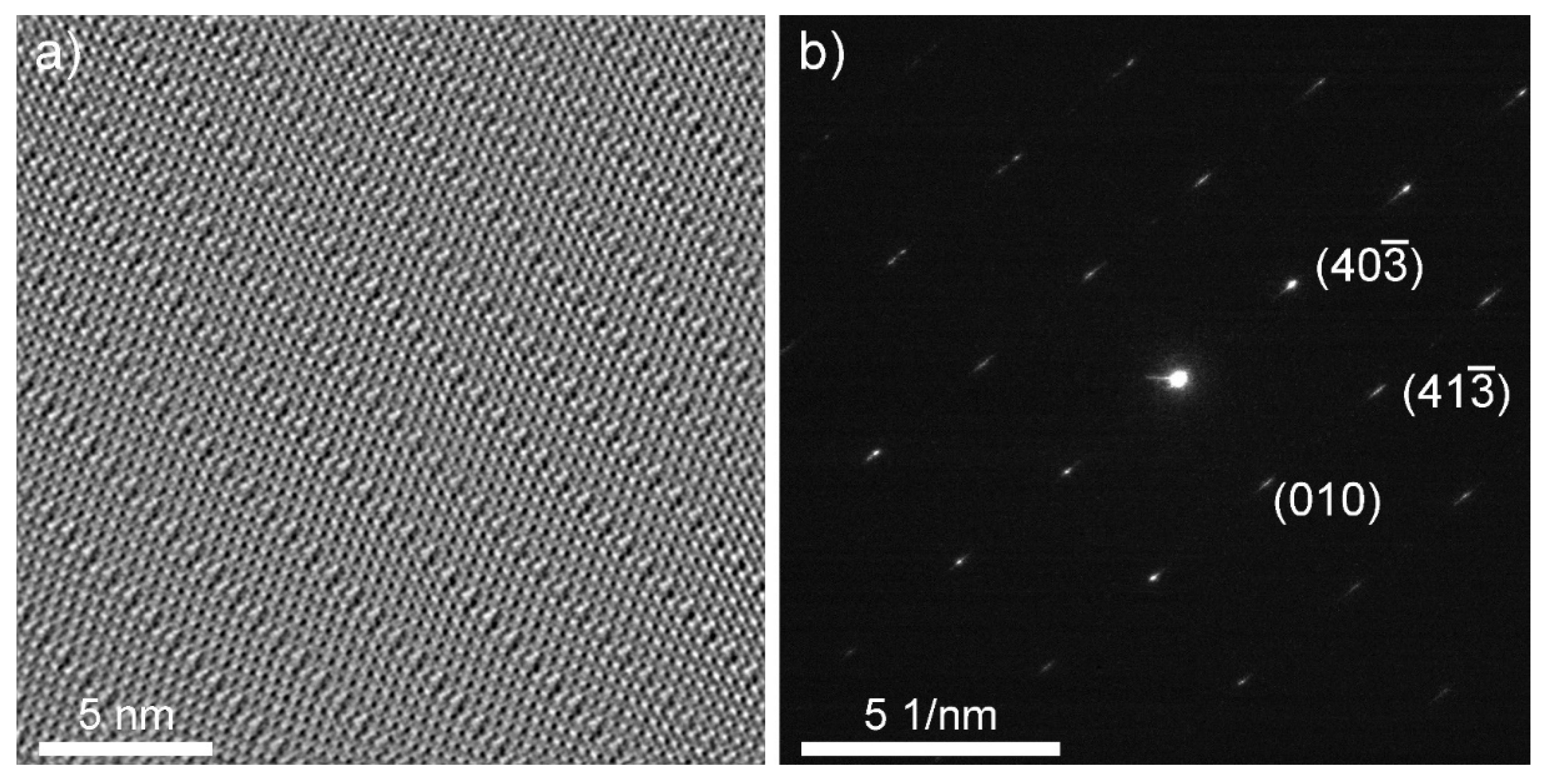
2.5. High-Resolution Transmission Electron Microscopy and Electron Diffraction

High-resolution transmission electron microscopy (HRTEM) and electron diffraction (ED) images were acquired using a Cs probe-corrected TEM/STEM JEOL ARM 200CF (JEOL, Peabody, MA, USA) microscope equipped with a cold-FEG electron source, operating at 200 kV. Distances between atomic columns and angles between their rows were measured using Digital Micrograph software. An accuracy of 0.04 Å in distance and 0.5° in angle was achieved. All HRTEM images were filtered using the Average Background Subtraction Filter method described in [18].

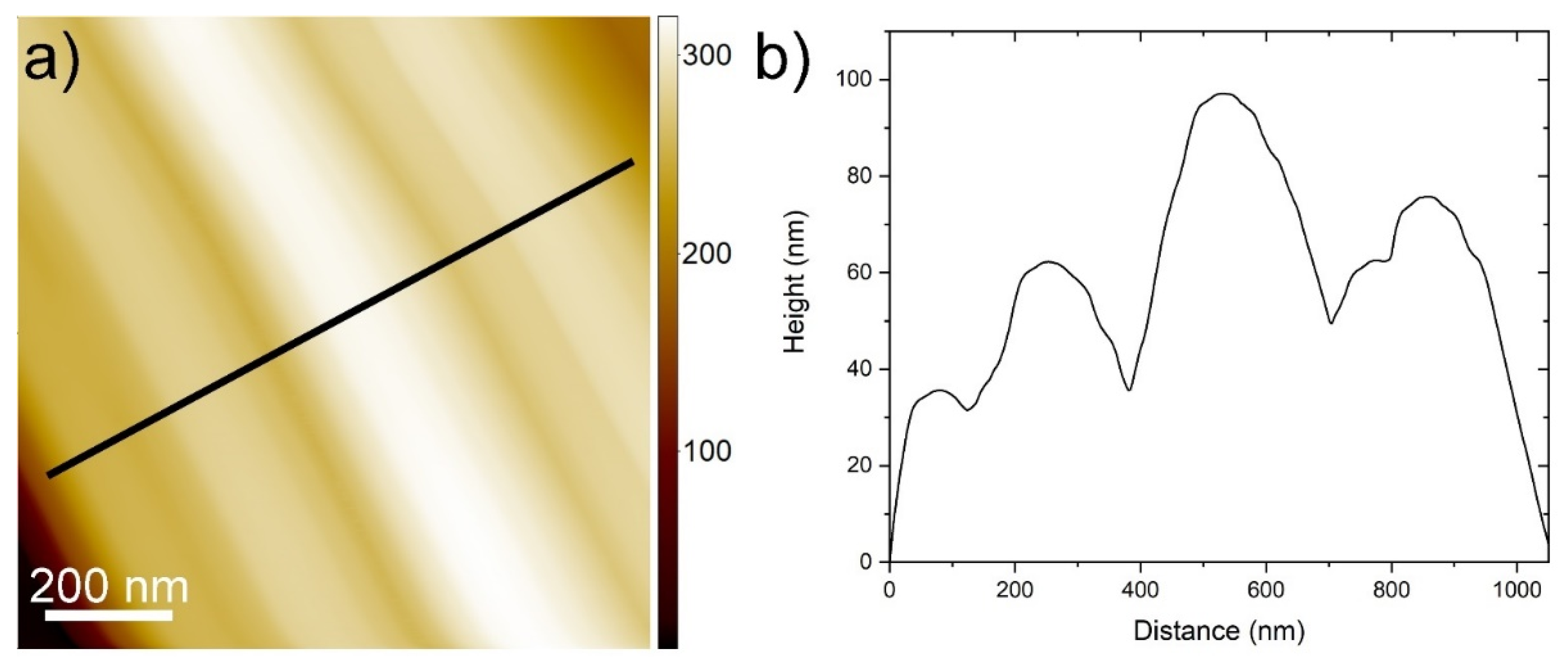
2.6. Atomic Force Microscopy

Atomic force microscopy (AFM) in contact mode was performed with an Omicron UHV VT-AFM (Scienta Omicron, Taunusstein, Germany) operating at 10−9 mbar. Silicon Cantilevers CSG10 (NT-MDT, Moscow, Russia) with a typical force constant of 0.11 N/m were used.

2.7. X-ray Photoelectron Spectroscopy

X-ray photoelectron spectroscopy XPS analysis was carried out on the PHI-TFA XPS spectrometer produced by Physical Electronics, Chanhassen, MN, USA. Samples were mounted on the metallic sample holder and introduced in ultra-high vacuum spectrometer. The vacuum during the XPS analyses was in the range of 10−9 mbar. The analysed area was 0.4 mm in diameter and the analysed depth was about 3–5 nm. Sample surfaces were excited by X-ray radiation from monochromatic Al source at photon energy of 1486.6 eV. The high-energy resolution spectra were acquired with energy analyser operating at resolution of about 0.6 eV and pass energy of 29 eV. The accuracy of binding energies was about ±0.2 eV. Three places on every sample were analysed. High resolution spectra were fitted with Gauss-Lorentz functions and Shirley function was used for background removal. For the XPS measurements, the ethanol suspension of nanotiles was deposited on an oxidized Si wafer, dried at room temperature and inserted into ultra-high vacuum of the spectrometer.

3. Results

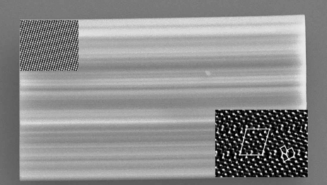
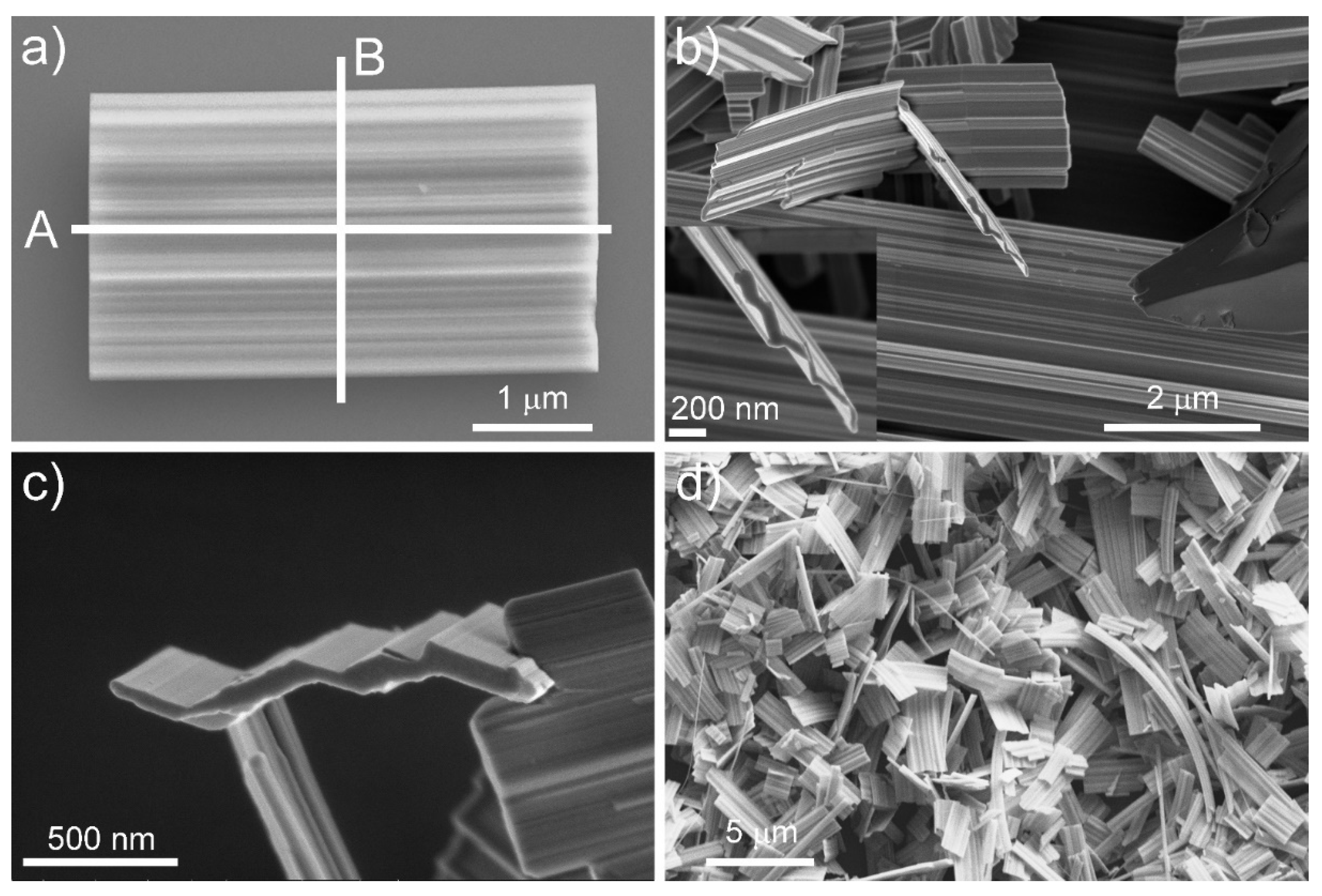
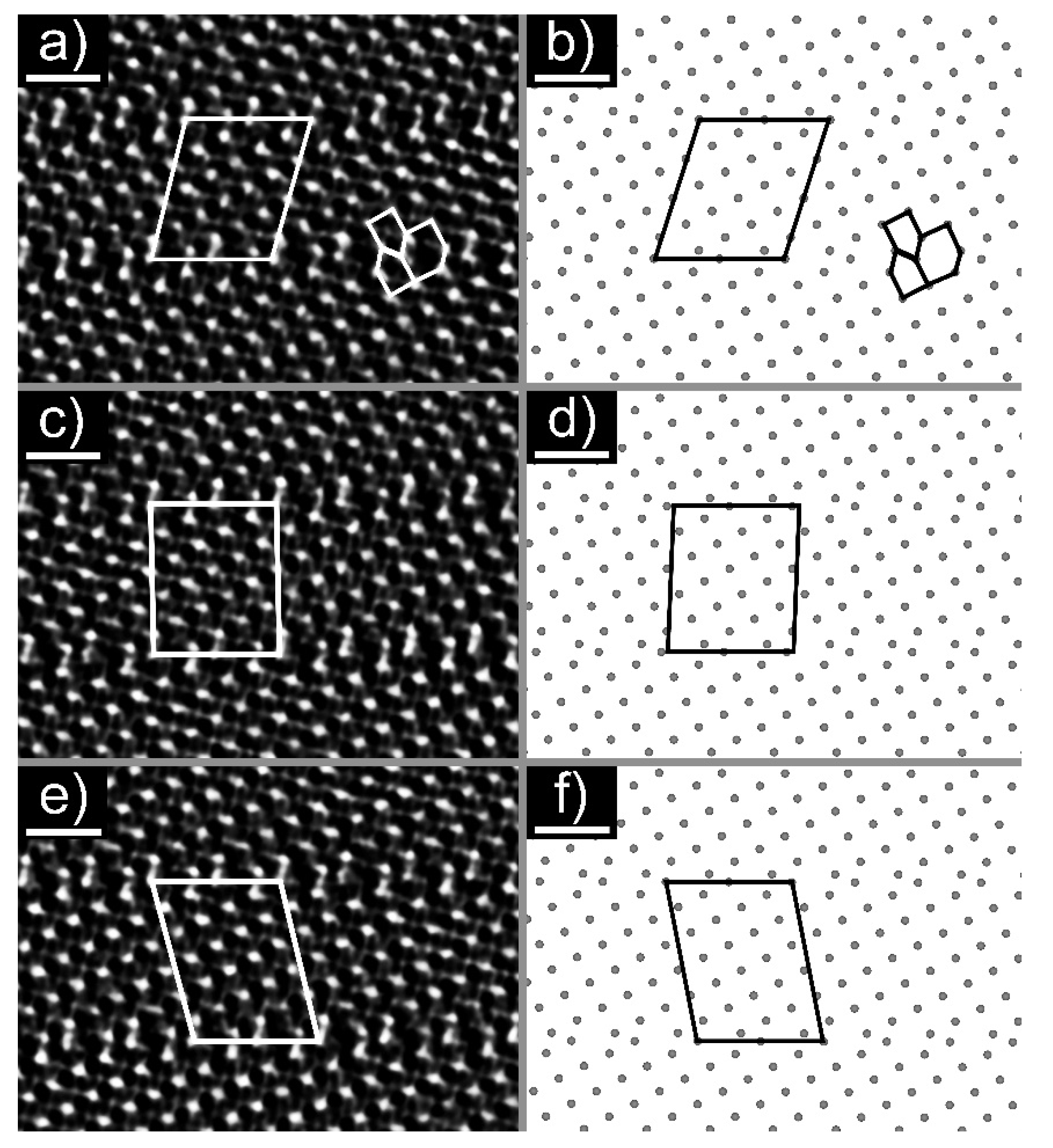
3.1. Electron Microscopy

The nanotiles, depicted in Figure 1, grow on the ampule walls in the form of a blue powder. A single nanotile usually grows in a rectangular shape, a few micrometres in width and up to 10 µm in length, as shown in Figure 1. The thickness of the nanotiles varies from a few 10 nm up to a few 100 nm, as seen in Figure S1 and Figure 1. They have distinct corrugations, which can be up to a few 10 nm deep, as seen in Figure 2. To determine the structure of the nanotiles, two cross-section lamellas perpendicular and parallel to the corrugations were prepared for further TEM analysis, as shown in Figure 1a.
An HRTEM image of the cross-section lamella B is shown in Figure 3a and Figure S2. Figure 3a was taken along the [010] direction, and was used to determine the stoichiometry of the nanotiles. The parallel contrast lines are crystallographic shear (CS) planes, which are characteristic for WnO3n−1 and WnO3n−2 phases. Only {102}r CS planes were observed, indicating that only WnO3n−1 structures grow inside the nanotiles [12,19]. Six stoichiometries were determined by measuring the unit cell parameters a, c, and β: W16O47 (WO2.938), W15O44 (WO2.933), W14O41 (WO2.928), W13O38 (WO2.923), W12O35 (WO2.917), and W11O32 (WO2.909), of which the last three were not experimentally observed to date [20]. The unit cell parameters a, c, and β of the observed phases are presented in Table 1. The a axis is oriented along the CS planes, while the c axis is directed towards the CS plane at the angle β, relative to axis a. An electron diffraction was performed on lamella A, Figure 3b. The reflections (010), ( 40 3 ¯ ) and ( 41 3 ¯ ) correspond to interlayer distances of 3.79 Å, 3.56 Å, and 2.61 Å, respectively. The first estimation of the unit cell parameter b was determined from the (010) reflection with the value of 3.79 Å. The second value for b (3.86 Å) was determined from the average distance between the tungsten atoms that are not part of the CS planes. The mean value of the unit cell parameter b is 3.83 Å. The theoretical tungsten atom positions and unit cell parameters for the newly observed phases were calculated using the model proposed in ref. [12]. The parameters d and e used in the model were determined from the HRTEM and electron diffraction images and are schematically shown in Figure S3: (i) interatomic distance between tungsten atoms that are not part of the CS plane that should equal unit cell parameter b (d = 3.83 Å); (ii) interatomic distance between tungsten atoms that are part of the CS plane, where the tungsten octahedra are joined by edges (e = 2.92 Å). The experimental unit cell parameters are in good agreement with the calculated ones. The unit cells are schematically drawn on the HRTEM and simulated structure images and are shown in Figure 4.

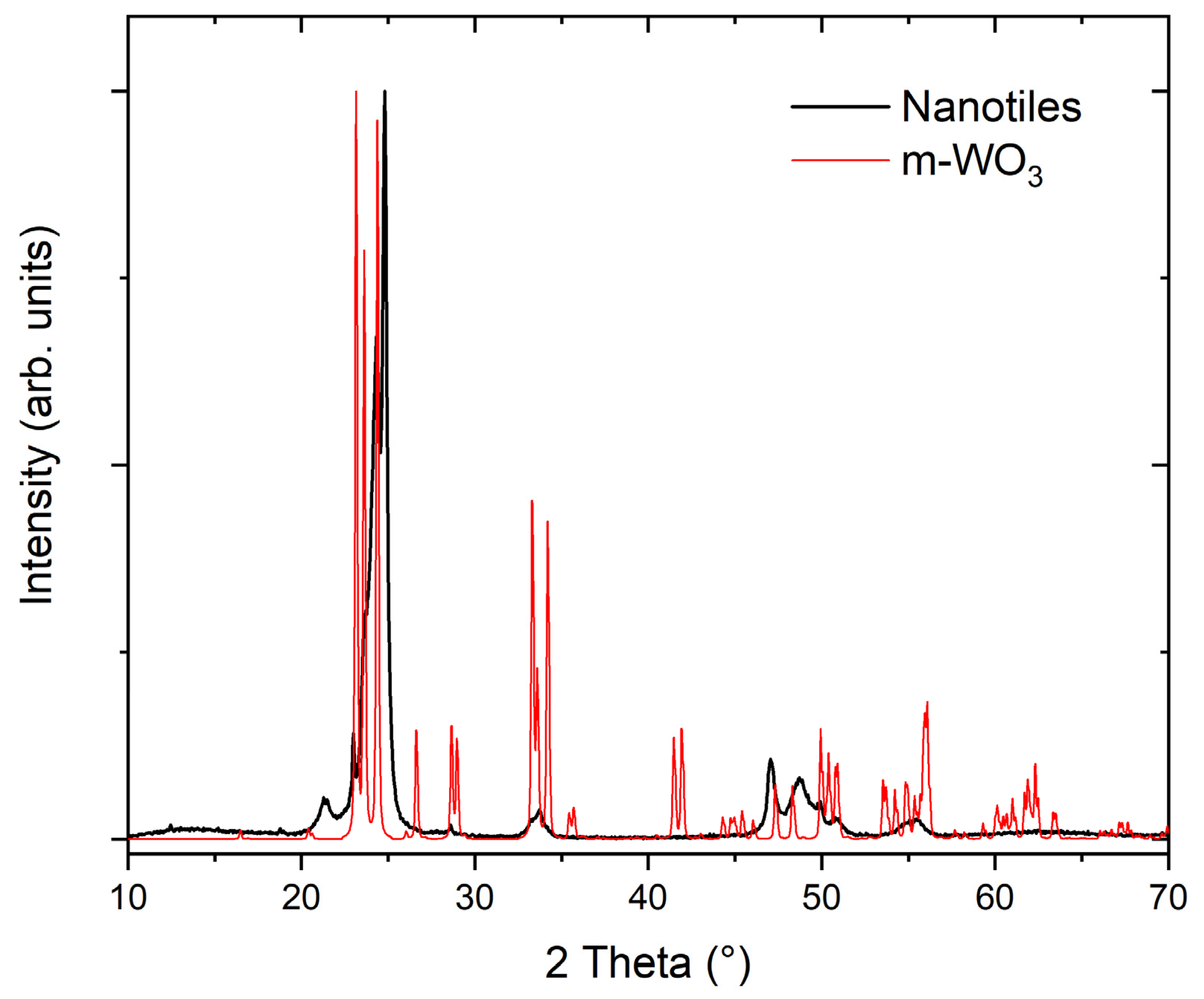
3.2. X-ray Diffraction

The XRD pattern of the nanotiles is shown in Figure 5. Due to their multi-stoichiometric structure, the XRD pattern is composed of diffraction lines corresponding to all tungsten suboxide phases present in the nanotiles. The low-angle diffraction lines were used to determine the most prominent phase, as they are different for each stoichiometry and do not overlap with the m-WO3 phase. The measured diffractogram had the best match with the W14O41 (WO2.928) stoichiometry, indicating that this is the phase the majority of the nanotiles crystallize in. The position of the diffraction lines, their relative intensities and the assigned (hkl) indices, are presented in Table 2. Additionally, the (010) line closely matches with the b unit cell parameter obtained from the HRTEM images. In Figure 5, the measured XRD pattern is compared to the m-WO3 one (PDF2: 01-072-1465).

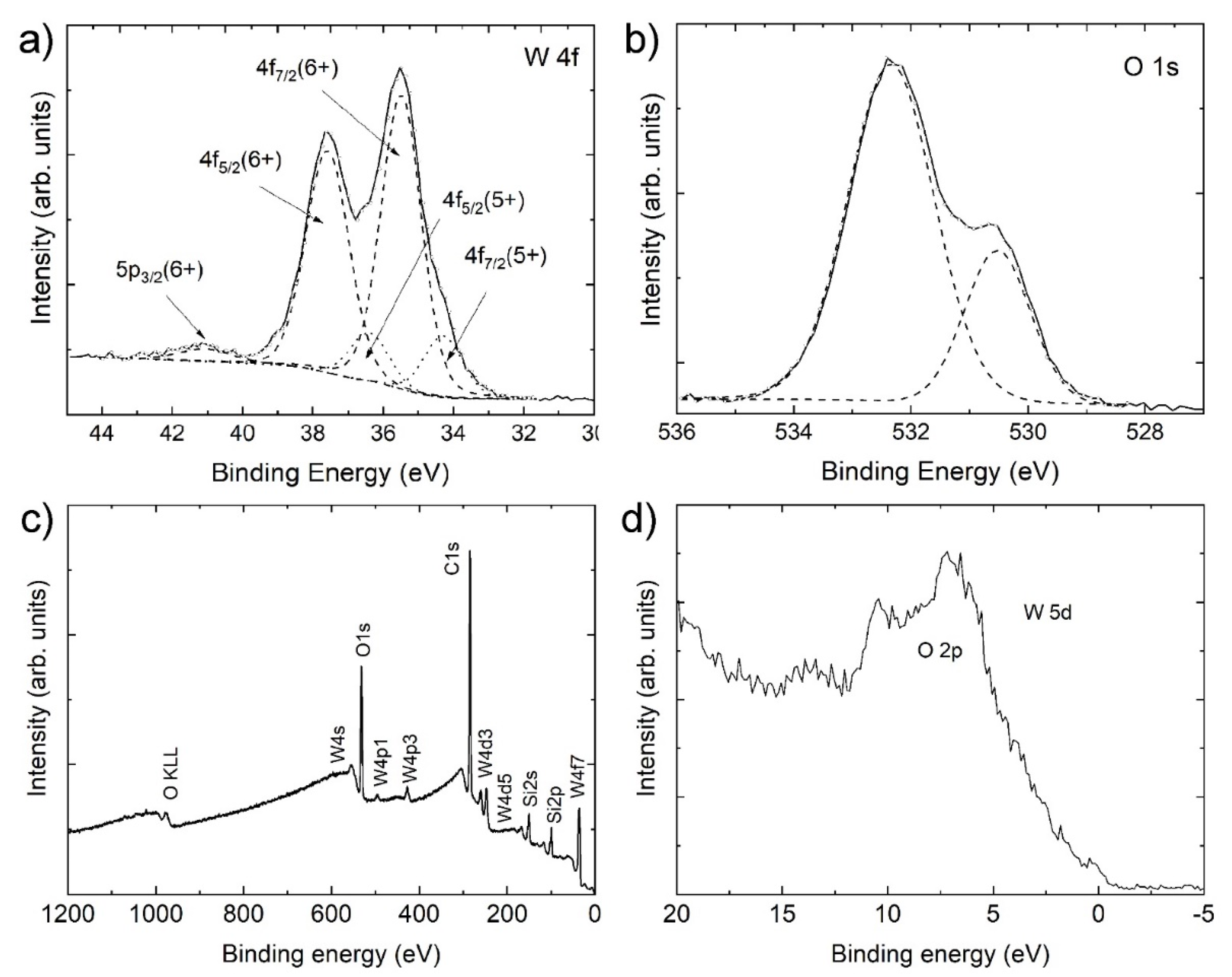
3.3. X-ray Photoelectron Spectroscopy

Figure 6 shows the W 4f and O 2p spectra, the survey spectrum, and the valence band spectrum of the nanotiles. The energy distribution of W 4f core levels is presented in Figure 6a. The spectrum can be deconvoluted into two doublets, with the additional fifth component (around 41.1 eV) corresponding to the W 5p photoelectrons. The main peaks, representing 84% of total W 4f, appear at 35.5 and 37.6 eV, corresponding to 4f7/2 and 4f5/2, respectively, of W in 6+ oxidation state [21]. The remaining 16% are attributed to a doublet positioned at 34.3 and 36.4 eV of the 4f7/2 and 4f5/2 of W in 5+ oxidation states [22,23]. We can disregard the presence of WO2 in the nanotiles, as there are no peaks corresponding to 4 + oxidation states (doublets at 33.3 and 35.5 eV) or metallic tungsten (31.2 and 33.4 eV) [24,25].
The oxygen O 1s spectrum can be deconvoluted into two peaks, as shown in Figure 6b. Peak at 530.5 eV, attributing 26% to the O 1s photoelectrons, corresponds to O2− bonded to W6+ in WO3 [26]. Peak at 532.3 eV may correspond to oxygen O2− bonded to SiO2 (substrate), C-O bonds or lower oxidation states of O in W-O bonds. The survey spectrum presented in Figure 6c shows no impurities other than carbon, while the silicon peaks arise due to the SiO2 substrate. The valence band spectrum presented in Figure 6d shows a broad O 2p peak with non-negligible density of states at the Fermi energy.

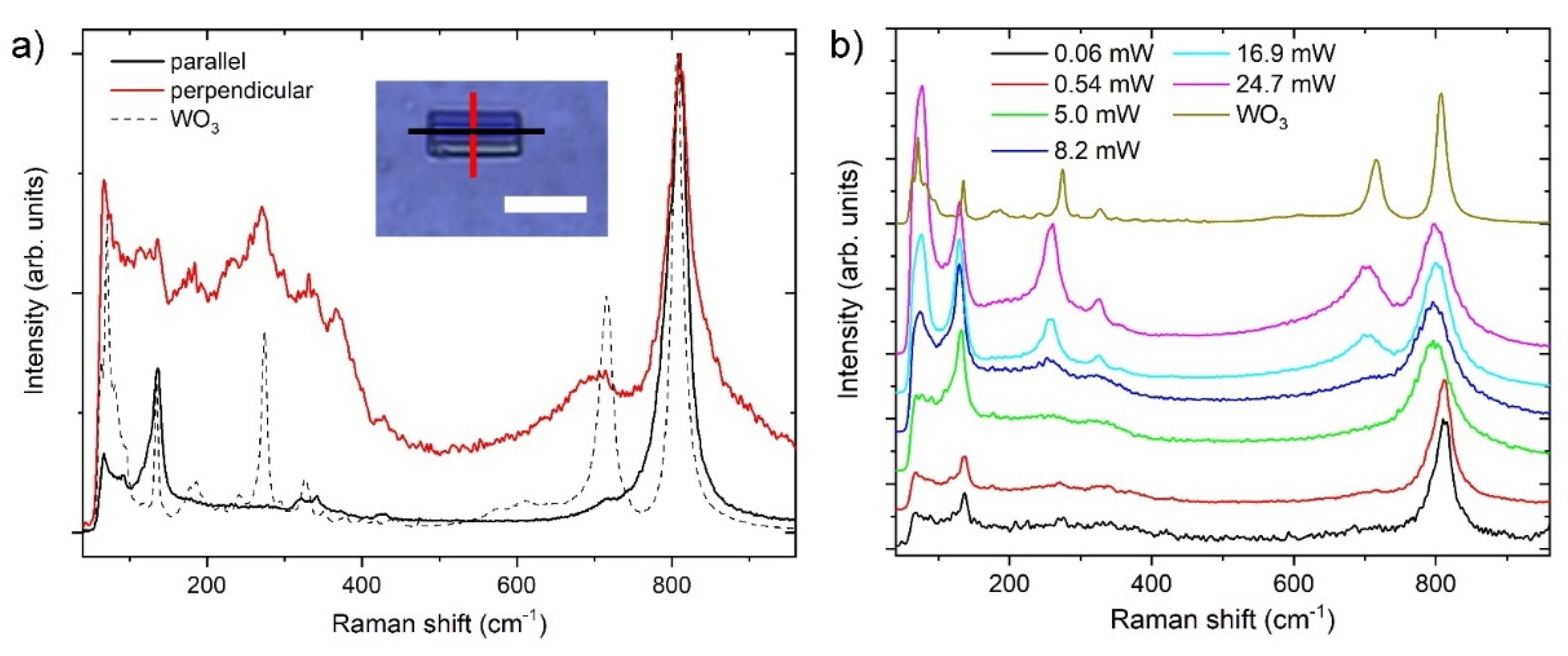
3.4. Raman Spectroscopy

Raman spectra of the nanotiles are shown in Figure 7a. The spectra were taken with the laser polarisation parallel and perpendicular to the corrugations (i.e., b axis). The peak positions and their normalized intensities are presented in Table 3. The Raman spectrum of the nanotiles with the polarisation parallel to the b axis reveals six peaks at 136.5, 322.5, 341.5, 426.5, 722, and 810 cm−1. The peak at 136.5 cm−1 is attributed to the relative translational or rotational motions of WO6 octahedral units in the same unit cell (lattice modes), the 322.5, 341.5, and 426.5 peaks to the W-O-W bending modes, while the 722 and 810 cm−1 peaks are attributed to the W-O stretching modes [7,27]. On the other hand, Raman spectrum of the nanotiles with the polarisation perpendicular to the b axis has nine peaks at 136, 180, 232.5, 271.5, 331.5, 367, 428, 702, and 810 cm−1. In both cases the 810 cm−1 peak is the most intense one. The dependency of the Raman spectra on orientation is a direct evidence of material anisotropy. Similarly to the previously reported spectra, [20] the spectrum where the polarisation is parallel to the b axis has sharper and more pronounced peaks, pointing to a crystal structure with fewer defects and a higher number of W-O bonds with well-defined lengths. The Raman spectrum recorded with the polarisation perpendicularly to the b axis has a greater number of peaks in the lattice (<200 cm−1) and bending mode (200–400 cm−1) region, while the peaks associated with W-O stretching modes (600–900 cm−1) are broader, indicating that multiple bond lengths are present [27,28]. The spectra of the nanotiles are compared with the precursor WO3 powder, with the most prominent peaks at 72, 135, 273, 372, 716, and 807 cm−1. These peaks match the monoclinic γ-phase with the space group P21/n, and the total of 48 Raman active modes [29]. Compared with the m-WO3 spectrum, the most intense peak at 810 cm−1 is slightly red-shifted towards longer wavelengths with regard to the 807 cm−1 in m-WO3, indicating slightly shorter bonds [7,30]. The peaks at 702 and 428 cm−1 are blue-shifted, indicating slightly longer bonds (i.e., shorter wavelengths) compared to the m-WO3 peaks situated at 715 cm−1 and 434 cm−1, respectively.
As these materials tend to be oxidized or damaged under the laser irradiation in ambient conditions, a stepwise laser power dependency measurement was performed. The powers at which the sample underwent change and damage can be easily inferred from the spectra shown in Figure 7b. The spectra in the power range between 0.06 and 0.54 mW are indistinguishable, while at 5 mW the 810 cm−1 peak shifts to 798 cm−1 and becomes broader, the 136 cm−1 peak becomes more intense and shifts to 130 cm−1, and the shoulders between 200 and 400 cm−1 become more prominent. At this point the sample remains visually undamaged, as concluded from its optical image. The power of 8.2 mW marks the start of the sample damage. This is accompanied with the peak at 130 cm−1 becoming the most prominent, the appearance of a new peak at 73 cm−1, and a shoulder appears around 710 cm−1. At 16.9 mW, the spectrum becomes very similar to that of the WO3 precursor, marking the complete oxidation of the nanotile due to the heating in ambient oxygen. This is evidenced by a clear appearance of the peak at 702 cm−1, albeit blue-shifted and broader (716 cm−1 for m-WO3). The two shoulders between 200 and 400 cm−1 transform into peaks at 258 and 325 cm−1 (274 and 327 cm−1 for m-WO3). Additionally, the peak at 76 cm−1 becomes the most intense one. For higher laser powers, no other new peaks appear.

4. Discussion

The reported nanotiles are composed of multiple WnO3n−1 phases, with three of those not observed to date. As previously reported, the multiphase nature of a single nanotile could stabilize the WnO3n−1 phases [20]. In our previous report, the similar multi-stoichiometric platelets had a flat, corrugation-free surface, while the nanotiles have distinct corrugations with tens of nm in depth. The change in the morphology could be explained with a slightly different overall stoichiometry. Another reason for this change may be because the nanotiles did not have a template from which to grow, while the platelets grew epitaxially from a nanowire [20]. Similar corrugations are also present in other tungsten suboxides [31,32,33] and could contribute to the stabilization of different phases. It is presumed that the nanotiles grow faster along the [010] crystallographic axis (along the corrugations), as the length of the nanotiles varies, while the width is remaining quite uniform.
The XRD pattern of the nanotiles differs from a typical XRD pattern of the m-WO3 especially in the low-angle region. Due to the P2/a symmetry of the WnO3n−1 stoichiometries, only (2n,0,l) and (2n,0,0) diffraction lines should be visible [12]. At approximately 2θ > 30°, diffraction lines from WnO3n−1 and m-WO3 overlap and thus cannot be used to determine the structure or the stoichiometry.
The valence band spectrum shows some density of states at the Fermi energy. The near-Fermi bands are formed due to 5d- and W 6s-like states taking part in the formation of the shortened W-W bonds [34] or due to trap states created by defects [35]. This could indicate a slightly metallic behaviour at room temperature, instead of a semiconducting one. DFT calculation on similar stoichiometries shows that the 5d-orbitals of tungsten atoms, which are part of the CS planes, are responsible for the conductivity and other effects related to the states near the Fermi surface [17,36].
The Raman spectra of the nanotiles have peaks of similar shape and position to those from the literature [20]. The spectra taken at the polarisation along the b axis have fewer peaks in the lattice and bending mode region than when the polarisation is perpendicular to the b axis. Compared to some other Raman spectra of WO3−x nanomaterials [24,37,38], our spectra show narrower peaks, pointing to a higher degree of crystallinity. When the laser power is increased, the nanotiles oxidize to m-WO3 [24,37].
Due to the intrinsic oxygen vacancies and formation of CS planes, the electronic and optical properties of tungsten suboxides differ from m-WO3. Such properties may provide an advantage in applications such as water splitting [39], near-infrared shielding [40], in anode materials for high-performance Li-ion batteries [41], field-effect-transistors [42], photocatalysis [43], and in-domain boundary engineering [44]. As it was shown [35], sub-stoichiometric WO3−x nanosheets can be used as physisorption-based NO2 sensors. A slight difference in the stoichiometry can change the WO3−x materials from a semiconductor to a metal, which can result in a poorer performance of such sensors. As pristine WO3 does not have a high photocatalytic activity, introducing oxygen vacancies and/or using lower dimensional WO3−x can improve its performance. In several studies [45,46], the WO3−x materials outperformed pristine WO3 in the degradation of dyes such as methylene blue, congo red, and rhodamine B. The oxygen vacancies act as electron donors, increasing the charge transport and thus enhancing the photocatalytic activity. Sub-stoichiometric materials also outperform m-WO3 when it comes to water splitting [47]. By annealing the samples under different atmospheres, the number and nature of oxygen vacancies were altered. It was concluded that the moderate concentration of oxygen vacancies results in appearance of W5+ shallow donor states that increase photoactivity, while the deep trap W4+ states have a detrimental effect on photocurrent. Being able to determine the stoichiometry and with it the electrical and optical properties of WO3−x nanomaterials offers new opportunities for a wide range of applications.

5. Conclusions

Multi-stoichiometric nanotiles were synthesized using the CVT method. The thickness of the nanotiles ranged from a few 10 to a few 100 nm, and they grew up to a few µm in the lateral size. The formation of {102}r CS planes indicates, that only WnO3n−1 phases grow inside the nanotiles. Three new stoichiometries were identified from HRTEM images: W13O38 (WO2.923), W12O35 (WO2.917), and W11O32 (WO2.909). Measured unit cell parameters agreed well with the calculated ones. The valence band spectrum showed some density of states at the Fermi energy, making the material slightly metallic. Obtained Raman spectra showed multiple peaks and are direct evidence of the material anisotropy. Increasing the laser power during Raman spectroscopy promoted the oxidation of the platelets into m-WO3.

Supplementary Materials

The following are available online at https://www.mdpi.com/article/10.3390/nano11081985/s1, Figure S1: (a) An AFM image of a nanotile with a line profile showing its height; (b) Figure S2: TEM image along the [010] direction. The white arrows point along the CS planes. Figure S3: interatomic distance between tungsten atoms that are not part of the CS plane (red) and interatomic distance between tungsten atoms that are part of the CS plane, where the tungsten octahedra are joined by edges (green).

Author Contributions

Conceptualization, L.P. and B.V.; methodology, L.P. and B.V.; validation, L.P., B.V., J.K., S.D.Š. and M.R.; formal analysis, L.P. and B.V.; investigation, L.P., B.V., J.K. and S.D.Š.; resources, M.R.; data curation, L.P. and B.V.; writing—original draft preparation, L.P. and B.V.; writing—review and editing, J.K., S.D.Š. and M.R.; visualization, L.P. and B.V.; supervision, M.R.; project administration, M.R.; funding acquisition, M.R. All authors have read and agreed to the published version of the manuscript.

Funding

This work was supported by grants from the Slovene Research Agency P1-0099 and P2-0082.

Data Availability Statement

The data presented in this study are available on request from the corresponding author.

Acknowledgments

The authors would like to thank Janez Jelenc for all the help regarding the AFM images.

Conflicts of Interest

The authors declare that they have no conflict of interest.

References

  1. Sayama, K.; Kazuaki, M.; Ryu, A.; Yoshimoto, A.; Hironori, A. Stoichiometric water splitting into H2 and O2 using a mixture of two different photocatalysts and an IO3/I shuttle redox mediator under visible light irradiation. Chem. Comm. 2001, 23, 2416–2417. [Google Scholar] [CrossRef]
  2. Ho, J. Novel nitrogen monoxides (NO) gas sensors integrated with tungsten trioxide (WO3)/pin structure for room temperature operation. Solid-State Electron. 2003, 47, 827–830. [Google Scholar] [CrossRef]
  3. Reyes, L.F.; Hoel, A.; Saukko, S.; Heszler, P.; Lantto, V.; Granqvist, C.G. Gas sensor response of pure and activated WO3 nanoparticle films made by advanced reactive gas deposition. Sens. Actuators B Chem. 2006, 117, 128–134. [Google Scholar] [CrossRef]
  4. Hai, Z.; Wei, Z.; Xue, C.; Xu, H.; Verpoort, F. Nanostructured tungsten oxide thin film devices: From optoelectronics and ionics to iontronics. J. Mater. Chem. 2019, 7, 12968–12990. [Google Scholar] [CrossRef]
  5. Thind, S.S.; Chang, X.; Wentzell, J.S.; Chen, A. High-performance based supercapacitor on tantalum iridium oxides supported on tungsten oxide nanoplatelets. Electrochem. Commun. 2016, 67, 1–5. [Google Scholar] [CrossRef]
  6. Cazzanelli, E.; Vinegoni, C.; Mariotto, G.; Kuzmin, A.; Purans, J. Low-Temperature Polymorphism in Tungsten Trioxide Powders and Its Dependence on Mechanical Treatments. J. Solid State Chem. 1999, 143, 24–32. [Google Scholar] [CrossRef] [Green Version]
  7. Daniel, M.F.; Desbat, B.; Lassegues, J.C.; Gerand, B.; Figlarz, M. Infrared and raman study of WO3 tungsten trioxides and WO3, xH2O tungsten trioxide tydrates. J. Solid State Chem. 1987, 67, 235–247. [Google Scholar] [CrossRef]
  8. Filipescu, M.; Ion, V.; Colceag, D.; Ossi, P.M.; Dinescu, M. Growth and characterizations of nanostructured tungsten oxides. Rom. Rep. Phys. 2012, 64, 1213–1225. [Google Scholar]
  9. Salje, E. Lattice Dynamics of WO3. Acta Crystallogr. Sect. A Cryst. Phys. Diffr. Theor. Gen. Crystallogr. 1975, 31, 360–363. [Google Scholar] [CrossRef]
  10. Li, X.L.; Liu, J.F.; Li, Y.D. Large-scale synthesis of tungsten oxide nanowires with high aspect ratio. Inorg. Chem. 2003, 42, 921–924. [Google Scholar] [CrossRef]
  11. Hariharan, V.; Gnanavel, B.; Sathiyapriya, R.; Aroulmoji, V. A review on tungsten oxide (WO3) and their derivatives for sensor applications. Int. J. Adv. Sci. Eng 2019, 5, 1163–1168. [Google Scholar] [CrossRef]
  12. Magnéli, A. Structures of the ReO3-type with recurrent dislocations of atoms:homologous series’ of molybdenum and tungsten oxides. Acta Crystallogr. 1953, 6, 495–500. [Google Scholar] [CrossRef] [Green Version]
  13. Pickering, R.; Tilley, R.J.D. An electron microscpe study of tungsten oxides in the composition range WO2.90–WO2.72. J. Solid State Chem. 1976, 16, 247–255. [Google Scholar] [CrossRef]
  14. Lundberg, M.; Sundberg, M.; Magnéli, A. The “Pentagonal Column” as a building unit in crystal and defect structures of some groups of transition metal compounds. J. Solid State Chem. 1982, 44, 32–40. [Google Scholar] [CrossRef]
  15. Migas, D.B.; Shaposhnikov, V.L.; Rodin, V.N.; Borisenko, V.E. Tungsten oxides. I. Effects of oxygen vacancies and doping on electronic and optical properties of different phases of WO3. J. Appl. Phys. 2010, 108, 093713. [Google Scholar] [CrossRef]
  16. Frey, G.L.; Rothschild, A.; Sloan, J.; Rosentsveig, R.; Popovitz-Biro, R.; Tenne, R. Investigations of nonstoichiometric tungsten oxide nanoparticles. J. Solid State Chem. 2001, 162, 300–314. [Google Scholar] [CrossRef]
  17. Migas, D.B.; Shaposhnikov, V.L.; Borisenko, V.E. Tungsten oxides. II The metallic nature of Magnéli phases. J. Appl. Phys. 2010, 108, 093714. [Google Scholar] [CrossRef]
  18. Kilaas, R. Optimal and near-optimal filters in high-resolution electron microscopy. J. Microsc. 1998, 190, 45–51. [Google Scholar] [CrossRef]
  19. Bursill, L.A.; Hyde, B.G. CS Families drived from the ReO3 structure type: An electron microscope study of reduced WO3 and related pseudobinary systems. J. Solid State Chem. 1972, 14, 430–446. [Google Scholar] [CrossRef]
  20. Pirker, L.; Višić, B.; Škapin, S.D.; Dražić, G.; Kovač, J.; Remškar, M. Multi-stoichiometric quasi-two-dimensional WnO3n−1 tungsten oxides. Nanoscale 2020, 212, 15102–15114. [Google Scholar] [CrossRef]
  21. Leftheriotis, G.; Papaefthimiou, S.; Yianoulis, P.; Siokou, A.; Kefalas, D. Structural and electrochemical properties of opaque sol–gel deposited WO3 layers. Appl. Surf. Sci. 2003, 218, 276–281. [Google Scholar] [CrossRef]
  22. Katoh, M.; Takeda, Y. Chemical state analysis of tungsten and tungsten oxides using an electron probe microanalyzer. Jpn. J. Appl. Phys. 2004, 43, 7292. [Google Scholar] [CrossRef]
  23. Zhang, C.; Boudiba, A.; Navio, C.; Bittencourt, C.; Olivier, M.G.; Snyders, R.; Debliquy, M. Highly sensitive hydrogen sensors based on co-sputtered platinum-activated tungsten oxide films. Int. J. Hydrogen Energy 2011, 36, 1107–1114. [Google Scholar] [CrossRef]
  24. Lu, D.Y.; Chen, J.; Zhou, J.; Deng, S.Z.; Xu, N.S.; Xu, J.B. Raman spectroscopic study of oxidation and phase transition in W18O49 Nanowires. J. Raman Spectrosc. 2007, 38, 176–180. [Google Scholar] [CrossRef]
  25. Remškar, M.; Kovac, J.; Viršek, M.; Mrak, M.; Jesih, A.; Seabaugh, A. W5O14 nanowires. Adv. Funct. Mater. 2007, 17, 1974–1978. [Google Scholar] [CrossRef]
  26. Trapatseli, M.; Vernardou, D.; Tzanetakis, P.; Spanakis, E. Field emission properties of low-temperature, hydrothermally grown tungsten oxide. ACS Appl. Mater. Interfaces 2011, 3, 2726–2731. [Google Scholar] [CrossRef] [PubMed]
  27. Hardcastle, F.D.; Wachs, I.E. Determination of the molecular structures of tungstates by raman spectroscopy. J. Raman Spectrosc. 1995, 26, 397–405. [Google Scholar] [CrossRef]
  28. Gonzalez-Calbet, J.M.; Rosique-Perez, C.; Vallet-Regi, M.; Alario-Franco, M.A.; Rodríguez-Carvajal, J. Lithium insertion in reduced tungsten oxides. Solid State Ionics 1989, 32, 162–166. [Google Scholar] [CrossRef]
  29. Woodward, P.M.; Sleight, A.W.; Vogt, T. Structure refinement of triclinic tungsten trioxide. J.Phys. Chem. Solids 1995, 56, 1305–1315. [Google Scholar] [CrossRef]
  30. Thummavichai, K.; Wang, N.; Xu, F.; Rance, G.; Xia, Y.; Zhu, Y. In situ investigations of the phase change behaviour of tungsten oxide nanostructures. R. Soc. Open Sci. 2018, 5, 171932. [Google Scholar] [CrossRef] [Green Version]
  31. Saqib, M.; Jelenc, J.; Pirker, L.; Škapin, S.D.; De Pietro, L.; Ramsperger, U.; Knápek, A.; Müllerová, I.; Remškar, M. Field emission properties of single crystalline W5O14 and W18O49 nanowires. J. Electron. Spectros. Relat. Phenom. 2020, 241, 146837. [Google Scholar] [CrossRef]
  32. Zhang, Z.; Sheng, L.; Chen, L.; Zhang, Z.; Wang, Y. Atomic-scale observation of pressure-dependent reduction dynamics of W18O49 nanowires in an environmental TEM. Phys. Chem. Chem.Phys. 2017, 19, 16307. [Google Scholar] [CrossRef] [PubMed]
  33. Merchan-Merchan, W.; Farahani, M.F.; Moorhead-Rosenberg, Z. Electron beam induced formation of tungsten sub-oxide nanorods from flame-formed fragments. Micron 2014, 57, 23–30. [Google Scholar] [CrossRef]
  34. Khyzhun, O.Y. XPS, XES and XAS studies of the electronic structure of tungsten oxides. J. Alloys Compd. 2000, 305, 1–6. [Google Scholar] [CrossRef]
  35. Khan, H.; Zavabeti, A.; Wang, Y.; Harrison, C.J.; Carey, B.J.; Mohiuddin, M.; Chrimes, A.F.; De Castro, I.A.; Zhang, B.Y.; Sabri, Y.M.; et al. Quasi physisorptive two dimensional tungsten oxide nanosheets with extraordinary sensitivity and selectivity to NO2. Nanoscale 2017, 9, 19162–19175. [Google Scholar] [CrossRef]
  36. Korshunov, M.M.; Nekrasov, I.A.; Pavlov, N.S.; Slobodchikov, A.A. Band structure of tungsten oxide W20O58 with ideal octahedra. JETP Lett. 2021, 113, 57–60. [Google Scholar] [CrossRef]
  37. Chen, J.; Lu, D.; Zhang, W.; Xie, F.; Zhou, J.; Gong, L.; Liu, X.; Deng, S.; Xu, N. Synthesis and raman spectroscopic study of W20O58 nanowires. J. Phys. D 2008, 41, 115305. [Google Scholar] [CrossRef]
  38. Huang, P.; Kalyar, M.M.A.; Webster, R.F.; Cherns, D.; Ashfold, M.N.R. Tungsten oxide nanorod growth by pulsed laser deposition: Influence of substrate and process conditions. Nanoscale 2014, 6, 13586–13597. [Google Scholar] [CrossRef] [PubMed] [Green Version]
  39. Lee, Y.-J.; Lee, T.; Soon, A. Phase stability diagrams of group 6 Magnéli oxides and their implications for photon-assisted applications. Chem. Mater. 2019, 31, 4282–4290. [Google Scholar] [CrossRef]
  40. Zhao, Z.; Bai, Y.; Ning, W.; Fan, J.; Gu, Z.; Chang, H.; Yin, S. Effect of surfactants on the performance of 3D morphology W18O49 by solvothermal synthesis. Appl. Surf. Sci. 2019, 471, 537–544. [Google Scholar] [CrossRef]
  41. Li, Y.; Chang, K.; Tang, H.; Li, B.; Qin, Y.; Hou, Y.; Chang, Z. Preparation of oxygen-deficient WO3−x nanosheets and their characterization as anode materials for high-performance Li-ion batteries. Electrochim. Acta 2019, 298, 640–649. [Google Scholar] [CrossRef]
  42. Zhuiykov, S. Material characterisation and transistor function of quasi two dimensional sub-stoichiometric WO3−x nanoflakes. Mater. Lett. 2016, 165, 173–177. [Google Scholar] [CrossRef]
  43. Pan, K.; Shan, K.; Wei, S.; Li, K.; Zhu, J.; Siyal, S.H.; Wu, H.-H. Enhanced photocatalytic performance of WO3−x with oxygen vacancies via heterostructuring. Compos. Commun. 2019, 16, 106–110. [Google Scholar] [CrossRef]
  44. Salje, E.K.H. Polaronic states and superconductivity in WO3−x. Condens. Matter 2020, 5, 32. [Google Scholar] [CrossRef]
  45. Chen, S.; Xiao, Y.; Xie, W.; Wang, Y.; Hu, Z.; Zhang, W.; Zhao, H. Facile strategy for synthesizing non-stoichiometric monoclinic structured tungsten trioxide (WO3−x) with plasma resonance absorption and enhanced photocatalytic activity. Nanomaterials 2018, 8, 553. [Google Scholar] [CrossRef] [PubMed] [Green Version]
  46. Parthibavarman, M.; Karthik, M.; Prabhakaran, S. Facile and one step synthesis of WO3 nanorods and nanosheets as an efficient photocatalyst and humidity sensing material. Vaccum 2018, 155, 224–232. [Google Scholar] [CrossRef]
  47. Mohamed, A.M.; Amer, A.W.; AlQaradawi, S.Y.; Allam, N.K. On the nature of defect states in tungstate nanoflake arrays as promising photoanodes in solar fuel cells. Phys. Chem. Chem. Phys. 2016, 18, 22217–22223. [Google Scholar] [CrossRef] [PubMed]
Figure 1. (a) A single nanotile, with lines A and B representing the direction of the cross-sections for the TEM lamellas; (bd) SEM images of different nanotiles.
Nanomaterials 11 01985 g001
Figure 2. (a) An AFM image of a nanotile with a line profile showing corrugations in (b).
Nanomaterials 11 01985 g002
Figure 3. (a) HRTEM image along the [010] direction (lamella B). (b) An electron diffraction of the [304] zone (lamella A).
Nanomaterials 11 01985 g003
Figure 4. HRTEM images of: (a) W11O32, (c) W12O35, and (e) W13O38 with the proposed unit cell. The scale bar is 1 nm. Simulated structures of: (b) W11O32, (d) W12O35, and (f) W13O38 with the proposed unit cell.
Nanomaterials 11 01985 g004
Figure 5. XRD pattern of the WO3−x nanotiles and of m-WO3 (PDF2: 01-072-1465).
Nanomaterials 11 01985 g005
Figure 6. XPS spectra of the nanotiles: (a) the W 4f spectrum; (b) the O 1s spectrum; (c) XPS survey spectrum; and (d) the valence band spectrum.
Nanomaterials 11 01985 g006
Figure 7. (a) Raman spectra of the WO3−x nanotiles taken parallel and perpendicular to the corrugations, and of m-WO3 (dashed line). Inset shows an optical image of the nanotile with the red and black line representing the direction of the laser polarisation. (b) Power dependency of the Raman spectra.
Nanomaterials 11 01985 g007
Table 1. Measured and calculated unit cell parameters for observed phases.
MeasuredCalculated
Structurea (Å)b (Å)c (Å)β (°)a (Å)b (Å)c (Å)β (°)
W11O3217.33.8318.979.317.1>3.8319.272.2
W12O3517.33.8320.289.617.1>3.8320.087.9
W13O3817.33.8322.5103.717.1>3.8322.1101.5
W14O4117.33.8324.574.217.1>3.8324.672.0
W15O4317.33.8325.688.017.1>3.8325.284.4
W16O4717.33.8327.598.317.1>3.8326.995.7
Table 2. Measured XRD diffraction lines (positions in ° and Å) and their relative intensities compared with the calculated d values using parameters obtained from HRTEM images and the assigned (hkl) indices.
MeasuredTheoretical W14O41
2 Theta (°)d (Å)Rel. Int. Assigned Index (hkl)d (Å)
12.57.080.02 ( 20 3 ¯ ) 7.04
18.84.700.01(005)4.68
21.54.130.05(403)4.17
23.23.840.14(010)3.83
23.93.730.30(110)3.73
24.53.630.66(112)3.63
25.03.561.00 ( 40 2 ¯ ) 3.52
28.93.090.02(407)3.09
34.22.620.04 ( 21 5 ¯ ) 2.62
48.51.880.10 ( 71 2 ¯ ) 1.88
50.31.810.08(322)1.81
52.71.740.03 ( 12 5 ¯ ) 1.74
57.61.600.02 ( 52 2 ¯ ) 1.60
Table 3. Raman peak position and normalized intensity of the nanotiles and WO3.
ModesParallelPerpendicularWO3 Powder
Raman ShiftIntRaman ShiftIntRaman ShiftInt
710.65
Lattice modes136.50.261360.141350.29
1800.09186.50.06
232.5Sh2410.03
W-O bending 271.50.192730.41
322.50.02331.50.123270.07
341.50.033670.053500.02
4170.01
426.50.014280.024370.01
W-O stretching722sh7020.177160.49
8101.008101.008071.00
Publisher’s Note: MDPI stays neutral with regard to jurisdictional claims in published maps and institutional affiliations.

