Article

Low-Temperature Growth of ZnO Nanowires from Gravure-Printed ZnO Nanoparticle Seed Layers for Flexible Piezoelectric Devices

1
University Grenoble Alpes, University Savoie Mont Blanc, CNRS, Grenoble INP, IMEP-LaHC, F-38000 Grenoble, France
2
ENEA, Italian National Agency for New Technologies, Energy and Sustainable Economic Development, Portici Research Centre, P.le E. Fermi 1, Portici, I-80055 Naples, Italy
*
Authors to whom correspondence should be addressed.
These authors contributed equally to the work.
Nanomaterials 2021, 11(6), 1430; https://doi.org/10.3390/nano11061430
Submission received: 19 April 2021 / Revised: 10 May 2021 / Accepted: 19 May 2021 / Published: 28 May 2021
(This article belongs to the Special Issue ZnO Nanowires: Growth, Properties, and Energy Applications)

Abstract

:
Zinc oxide (ZnO) nanowires (NWs) are excellent candidates for the fabrication of energy harvesters, mechanical sensors, and piezotronic and piezophototronic devices. In order to integrate ZnO NWs into flexible devices, low-temperature fabrication methods are required that do not damage the plastic substrate. To date, the deposition of patterned ceramic thin films on flexible substrates is a difficult task to perform under vacuum-free conditions. Printing methods to deposit functional thin films offer many advantages, such as a low cost, low temperature, high throughput, and patterning at the same stage of deposition. Among printing techniques, gravure-based techniques are among the most attractive due to their ability to produce high quality results at high speeds and perform deposition over a large area. In this paper, we explore gravure printing as a cost-effective high-quality method to deposit thin ZnO seed layers on flexible polymer substrates. For the first time, we show that by following a chemical bath deposition (CBD) process, ZnO nanowires may be grown over gravure-printed ZnO nanoparticle seed layers. Piezo-response force microscopy (PFM) reveals the presence of a homogeneous distribution of Zn-polar domains in the NWs, and, by use of the data, the piezoelectric coefficient is estimated to be close to 4 pm/V. The overall results demonstrate that gravure printing is an appropriate method to deposit seed layers at a low temperature and to undertake the direct fabrication of flexible piezoelectric transducers that are based on ZnO nanowires. This work opens the possibility of manufacturing completely vacuum-free solution-based flexible piezoelectric devices.

Graphical Abstract

1. Introduction

Flexible piezoelectric transducers make the development of innovative devices possible, especially in the energy and sensor fields [1]. Several piezoelectric materials have been studied and integrated into flexible substrates, including organic materials, such as poly(vinylidene fluoride) (PVDF) [2] and its co-polymers [3,4,5]; inorganic materials, like lead zirconate titanate (PZT) [6], potassium sodium niobate (KNN) [7], lead magnesium niobate-lead titanate (PMN-PT) [8], barium titanate (BaTiO3) [9], zinc stannate (ZnSnO3) [10], and bismuth ferrite (BiFeO3) [11]; and semiconductors like zinc oxide (ZnO) in the shape of nanowires (NWs) [12,13]. Among those materials, ZnO has attracted a great deal of attention because it is biocompatible, abundant, and sustainable, making it interesting for future applications while reducing the use of critical and toxic materials [14]. In particular, ZnO NWs have been widely used in different applications related to the conversion of mechanical energy into electricity at the nanometric scale. Some advantages of these NWs, compared to the bulk counterpart, are the ability to withstand high deformation values without fracturing [15,16,17], high values for the Young’s modulus [18,19], and high values for the piezoelectric coefficient [20], as well as a high surface-to-volume ratio that allows enhanced piezoelectric responses thanks to Fermi-level pinning [21].
ZnO can exist in different miniaturized forms, like quantum dots, nanorods, nanowires, nanotubes, nanosheets, nanobelts, nanocones, and twinned disk structures [22]. The ability to form different shapes in miniature sizes, along with a high surface charge density, polarity, and orientation enables ZnO nanostructures to display various applications in the fields of gas sensing, energy storage, energy harvesting, photocatalysis, flexible electronics, optoelectronics, and environmental waste treatment, etc. The high surface area of ZnO NWs promotes greater interfacial adsorption and diffusion, which enhances their physical and chemical properties. ZnO has a wide band gap of 3.37 eV, which is one of the highest in the II-IV semiconductor metal oxides, and also has a large excitation binding energy of 60 meV [23].
These superior properties make ZnO NWs an interesting material to be adopted in the high-tech renewable energy field for the development of energy conversion or storage devices, as ZnO NWs meet the requirements for power and energy density [24]. Also, the low cost of fabrication, negligible emission of pollutants, and the possibility of enhancing energy conversion efficiency make ZnO NW-based devices economically viable for industrial production [25,26].
The first energy harvesting device based on ZnO NWs (then referred to as a nanogenerator—NG) was demonstrated in 2006 by Wang et al. [27]. Since then, a number of NG devices with different structures that are grown on flexible or rigid substrates have been investigated. Recently, in the field of flexible electronics, a great deal of effort has been focused on flexible NG devices, which can be used while experiencing bending [28,29,30] or compressive [31,32,33,34,35] forces in applications like material-based flexible electronic skins [36] or as nanocomposite-based sensors [37].
Chemical bath deposition (CBD) is a particularly popular method to grow piezoelectric nanostructures due to its ease of implementation, support to scale production, and moderate processing temperatures [33,38,39]. With low processing temperatures, the method is suitable for the use of flexible plastic substrates. Usually, the substrate is covered by a thin seed layer to promote growth and lower the thermodynamic nucleation barrier [40]. Once the seed layer is deposited, the substrates are immersed in a supersaturated growth solution at a moderate temperature for several hours. Using this technique, ZnO NWs or nanorods (NRs) have been grown over metallic [41,42,43] and polymeric materials [30,44,45], depending on the type of ZnO seed layer deposition. In this work, zinc nitrate hexahydrate (Zn(NO3)2.6H2O) and hexamethylenetetramine ((CH2)6N4) are used as precursors for the synthesis of ZnO NWs using the CBD process. Hexamethylenetetramine (HMTA) is a popular reagent that is used as a hydroxide anion (OH) precursor for ZnO synthesis [46].
To date, a large variety of techniques are used to obtain ZnO seed layers, such as RF sputtering, atomic layer deposition (ALD), spray pyrolysis, chemical vapor deposition, and wet chemical synthetic routes, including spin and dip coatings [47,48]; however, most of them are confined to a laboratory scale and require an additional procedure for preparing patterned layers through expensive and complex processes such as photolithography and etching [49]. Moreover, the typical synthetic routes usually require high temperature annealing post-treatment for improving the crystallinity of the ZnO seeds, thus excluding polymers from the choice of flexible substrates [50,51,52].
On the other hand, there has been an increasingly pressing demand for easy and cost-effective methods to prepare ZnO patterned seed layers at low temperatures [49,53], which is essential for the use of plastic substrates.
In the last decade, conventional printing processes have been highly regarded as additive techniques for easy, fast, and low-cost thin film deposition at ambient conditions [54,55]. Using these techniques, patterning is carried out simultaneously with the deposition, thus substantially reducing energy, time, and material consumption [56]. In addition, the typical low temperatures of solution processes make printing compatible with most flexible substrates [55,57]. Among printing techniques, gravure techniques are widely employed in many fields and applications thanks to the ability to couple high throughput and high quality [58,59]. Recently, gravure printing has been proven to support the production of uniform large-scale nanoparticulate ZnO thin films on flexible plastic substrates [60]. The quality of the deposited films is so high that it successfully allows subsequent ZnO sintering through an innovative method at a very low temperature and in pressure less conditions [61]. Several printing techniques have been used to deposit ZnO seed layers for the subsequent growth of ZnO NWs, although none of the reports show piezoelectric measurements with the grown NWs [57]. Furthermore, to the best of our knowledge, there have been no reports on the growth of ZnO NWs from layers deposited by gravure printing.
Gravure printing techniques rely on the direct transfer of a low-viscosity ink (1–100 mPas) from the micro-engraved cells of a cylinder to a flexible substrate by the pressure of a counter cylinder. This process can be considered as a sequence of sub-processes (inking, doctoring, transfer, spreading, and drying, as shown in Figure 1a–d) [60]. Essentially, at the microscopic level, the fluid dynamics of the gravure printing process are governed by the balance between viscous and surface tension forces, where the latter are the driving force [62].
In this study, gravure printing with crystalline ZnO nanoparticles (NPs) was attempted for the first time to produce a seed layer for ZnO NW growth (Figure 1e) from the perspective of flexible piezoelectric devices manufacturing. Using crystalline NPs as starting material allows the elimination of the thermal post-annealing step, making the process easier, time-effective, and compatible with polymeric substrates. Two morphologies of the seed layer were also produced (i.e., nanoparticulate and sintered) to investigate their influence on the density, the diameter, and the orientation of NW growth. The NWs grown from the gravure-printed seed layers were also compared with ZnO NWs grown from a seed layer deposited by ALD on a silicon substrate as a reference.
Piezoelectric properties, including the amplitude of the piezo-response and the phase of the grown NWs, were measured with the different samples via piezo-response force microscopy (PFM).

2. Experiments

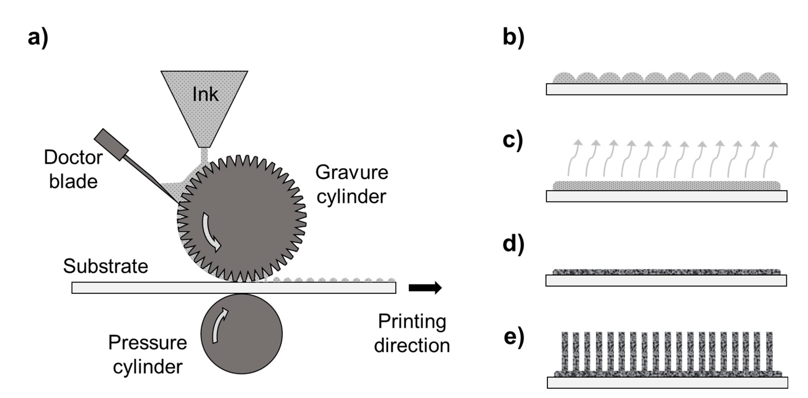
2.1. Seed Layer Deposition

A ZnO NP colloidal suspension (Sigma-Aldrich, St. Luis, MO, USA, particle size <130 nm) was used to prepare an ink, diluting the commercial suspension with ethanol (final concentration 8 wt %), for printing seed layers of a 55 ± 6 nm size onto a commercial indium tin oxide (ITO)/poly(ethylene terephthalate) (PET) (150 nm/125 µm) substrate (2 × 1.5 cm2) acquired from DuPont Teijin Films, Luxembourg.
Printing was performed using a lab-scale gravure printer (IGT G1-5, Amsterdam, the Netherland) equipped with a cylinder with a line density of 70 lines/cm, stylus angle of 120°, screen angle of 53°, and cell depth of 30 µm. All prints were performed in air at room temperature on corona-treated substrates. After preliminary tests, the best printing conditions were found to be a printing force of 500 N at a speed of 60 m/min. After printing, the samples were dried at 100 °C for one hour. The thickness of the dried printed layers above reported was investigated by an interferometry-based optical profilometer (Talysurf CCI HD, Taylor Hobson, Leicester, UK).
A set of ZnO NP printed samples were exposed to the vapor of 1 M acetic acid aqueous solutions for 4 h in a closed oven at 50 °C for inducing chemical bonds among the particles up to the sintering, as reported elsewhere [61].
A 40-nm-thick ZnO seed layer was also deposited on an ITO/Si (166 nm/375 µm) substrate (1.5 × 1.5 cm2) by ALD at 250 °C as previously reported [33]. These samples were prepared as references for the growth of ZnO NWs.

2.2. Growth of Nanowires

All ZnO NWs were grown under identical conditions by CBD. Samples grown on Si/ITO substrates were firstly cleaned with acetone, ethanol, and DI water in an ultrasonic bath for 5 min and dried with an N2 gun. For the seed layers prepared by gravure printing, the acetone and ethanol washing steps were omitted. Hexamethylenetetramine ((CH2)6N4, Sigma-Aldrich) and zinc nitrate hexahydrate (Zn(NO3)2.6H2O, Sigma-Aldrich, St. Luis, MO, USA) were dissolved in equimolar (50 mM) ratios in 150 mL of DI water at room temperature. The growth solution was stirred for 20 min at 1000 rpm and later put to rest for 40 min before decanting the clear solution into glass bottles. The substrates were fixed on cleaned glass slides with Kapton tape before being immersed face-down into the growth solution. The hydrothermal growth was carried out in an oven at 85 °C for 16 h. Later, the substrates were rinsed with DI water and dried with an N2 gun before being stored for surface characterization.

2.3. Structural Property Measurement

The printed films were morphologically characterized by atomic force microscopy (AFM) and scanning electron microscopy (SEM). AFM analysis was carried out using the Veeco Dimension Digital Instruments Nanoscope IV, New York, NY, USA.
Plainview, NY 11803 apparatus in the tapping mode configuration. For the SEM investigations of the gravure films, a field emission scanning electron microscope (FEG-SEM, Leo 1530 Gemini by Zeiss, Oberkochen, Germany) was used with an operating voltage of 7–9 kV.
Raman spectroscopy was carried out by a Renishaw InVia Reflex (Renishaw, Torino, IT) spectrometer selecting the laser wavelength of 514.5 nm (laser power of 100%) and an objective of 50× for magnification. The investigated wavelength range was 300–800 cm−1. For each measurement, 30 subsequent accumulations and an exposure time of 10 s were set. For each type of sample, ten measurements were taken in order to verify their homogeneity.

2.4. Piezoelectric and Polarity Measurement

A Bruker Dimension Icon (Santa Barbara, CA, USA) atomic force microscope instrument was used to carry out the PFM measurements on the ZnO NWs. A PtSi noncontact high-resonance frequency (NCH) tip with a high spring constant value (range values among 43–50 N/m) was used in the measurements. The PtSi-NCH tip was chosen to perform the PFM measurement as it allows a reduction of the electrostatic force involved in the piezoelectric signal [63,64]. The applied AC bias was fixed at 5 V, and the frequency was kept at 14 kHz to avoid any electrostatic contribution (typically above 50 kHz) as shown in the amplitude and phase vs. frequency plots (see Figure S1). To avoid collisions and lateral bending of the vertically grown NWs with the AFM tip, the classical contact mode PFM was not used in this study. Instead, the DataCube mode was used to measure the amplitude and phase (see the details in the Supplementary Material, including Figures S2 and S3).

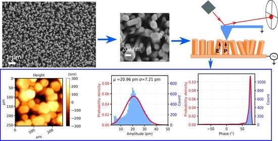
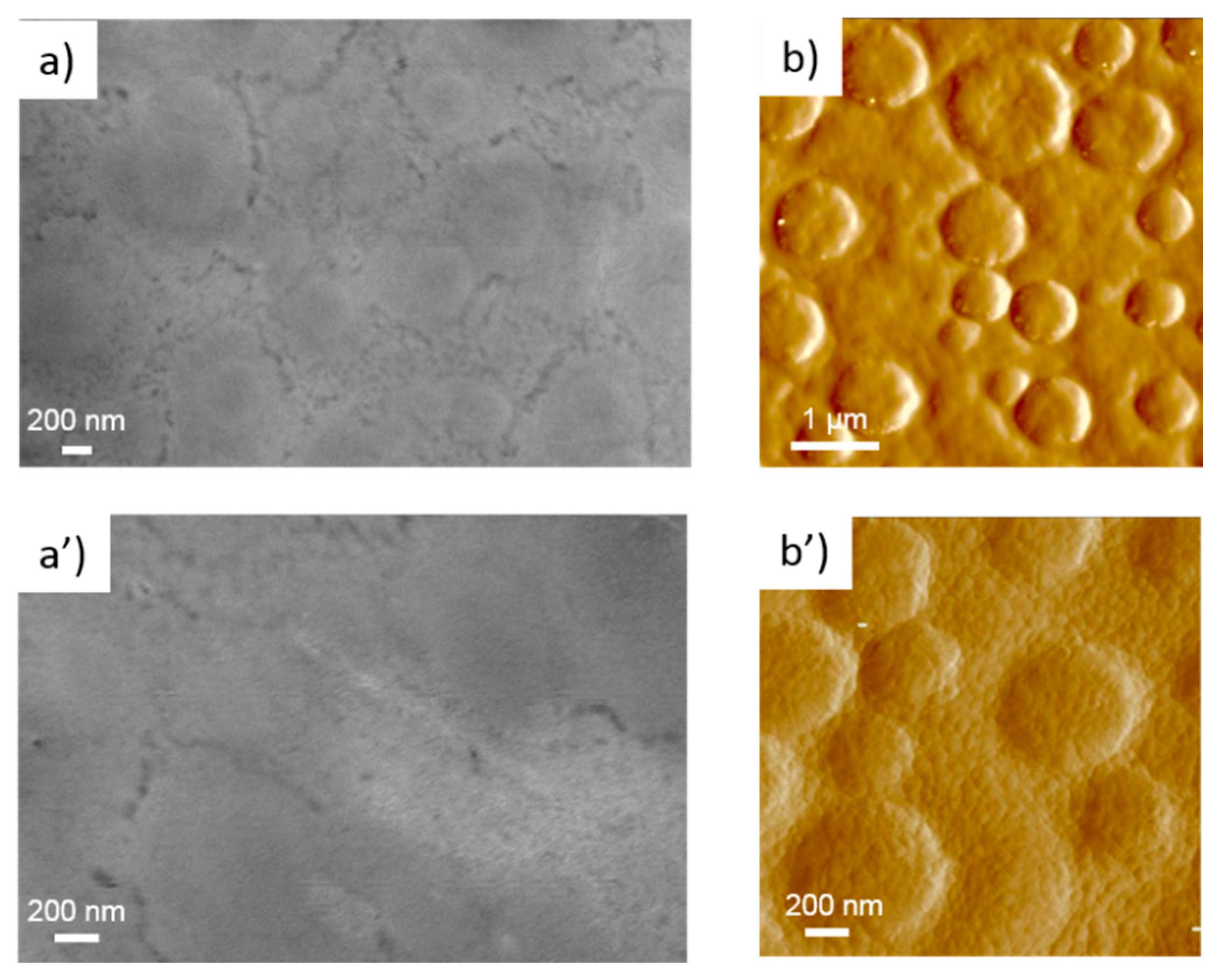
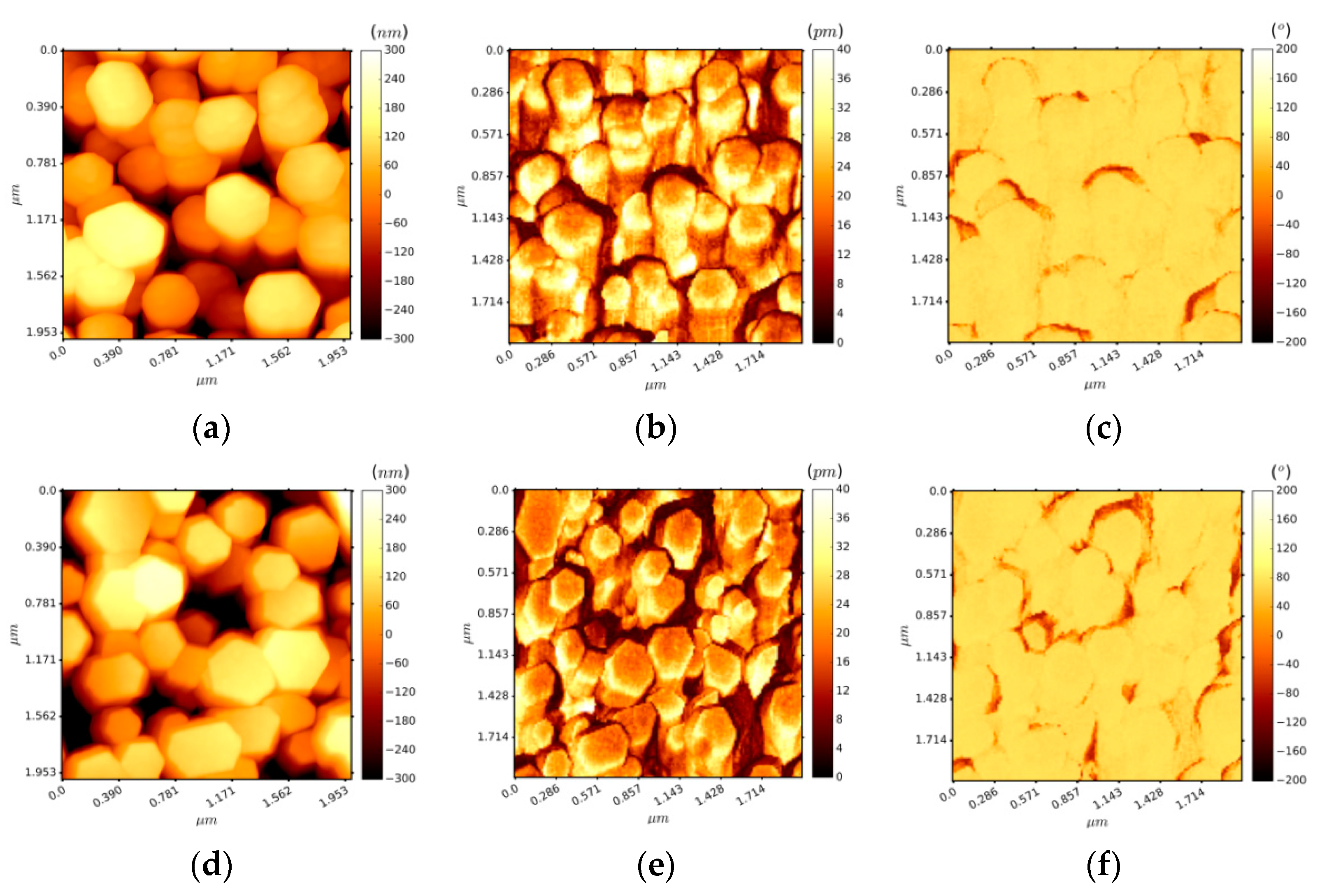
3. Results and Discussion

In this work, gravure printing was investigated regarding the deposition of ZnO seed layers for the subsequent growth of NWs. On the base of a previous study [60], it was possible to obtain a very smooth, continuous, and homogeneous thin film of nanoparticulate ZnO seeds printed onto an ITO-coated PET substrate (see details in the Supplementary Material, including Table S1 and Figure S4). After printing, some of the printed samples were exposed to a vapor annealing sintering treatment at a very low temperature (50 °C) to investigate the effect of the seed layer morphology on NW growth.
Figure 2 and Figure 3 show SEM and AFM images of the printed ZnO seed layers exposed at different annealing times of 0 and 4 h, respectively. The surface morphology changed from close-packed nanoparticulate film (as-printed) up to a dense one (sintered) over time. Indeed, thanks to a dissolution-reprecipitation mechanism during acidic vapor annealing, the chemical bonds among NPs merge particles as per a grain growth phenomenon. From these SEM images, the measured grain size in the non-sintered layers was 45 ± 12 nm. Concerning the sintered samples, although the evaluation was complex because the grain borders were not well defined, the measured values changed drastically with respect to the non-sintered layers. By the SEM analysis, the grain size ranges from 500 nm to 1000 nm with an estimated average of 547 ± 450 nm.
NWs were grown by a CBD method on both types of printed ZnO seed layers. Moreover, in order to obtain reference samples, NW growth was also performed on a Si/ITO/ZnO substrate where a ZnO seed layer was deposited by ALD. In Figure 4a–c, SEM images of the ZnO NWs on the different seed layers are shown. In Figure 4a’–c’, magnified images of the ZnO NWs are shown in a similar sequence. The ZnO NWs that were grown on the ZnO (ALD)/ITO/Si and the as-printed (not sintered) ZnO seed layer/ITO/PET substrates have average diameters of nearly 199 nm and 210 nm and standard deviations of nearly 86 nm and 84 nm, respectively. Histograms of these measurements are shown in Figure S5a,b. The ZnO NWs were closely packed and showed good vertical alignment. The obtained ZnO NWs had relatively small diameters and good alignment, which is important in piezoelectric applications [21], in particular when taking into account the following: (i) low temperature techniques of seed layer deposition; (ii) deposition on flexible substrates; and (iii) the use of non-expensive chemical methods without the requirement of a vacuum (see Table S2). In Figure 4c, it may be observed that the ZnO NWs were sparsely packed and featured random growth orientations. There was a drastic change in the dimensions of the ZnO NWs, with an average diameter of 987 nm and standard deviation of 250 nm (see Figure S5c). Figure S6a,b shows cross-sectional SEM images of ZnO NWs grown on the ITO/Si and ITO/PET substrates, respectively. It was estimated that the ZnO NWs were nearly 3.5 µm in length. It can be observed that during the growth process of ZnO NWs, some of the NWs merged. The screw-like tops of the ZnO NWs in Figure 4c indicates that their growth followed a screw dislocation nucleation mechanism along the axial direction [65].
As can be seen, the growth of NWs appeared to be significantly affected by the morphology of the seed layer, as also stated in the literature [66,67,68]; however, the relationships between the seed layer characteristics and NW growth have not been clearly established as of yet. In particular, the seed layer thickness, orientation, and grain size have key roles on the vertical growth of ZnO NWs. As known, ZnO preferentially crystallizes in a hexagonal polar wurtzite structure [69]. The ZnO NW growth direction by CBD occurs predominantly along the polar direction of the seed layer, which provides nucleation sites [66,67].
A possible explanation for the observed results may be proposed on a thermodynamic basis, considering the processes driven by the minimization of the overall system energy. In particular, the seed layer energy governs the nucleation process and subsequently determines the density of ZnO NWs.
In general, the energy of a particle is a function of the size, shape, stress, and external environment [70]. In a NP, a significant number of atoms are localized at the surface [69]. The additional energetic term due to the high-energy under-coordinated atoms at the surface is described as the surface free energy [71,72] and becomes increasingly larger as particle size decreases. In addition, several surface defects [70,73,74] may be present, especially when the particle size is very small [75], resulting in a further increase in the particle free energy [76]. As such, due to their high energy, NPs typically show a higher reactivity compared to bulk or micrometric particles [77,78]. As a result, a highly energetic as-printed nanoparticulate seed layer can be especially chemically reactive for ZnO NW nucleation. In addition, a NP seed alignment mechanism may be present during the CBD, furthering contributing to the high NW density. As shown in Figure 2, the as-printed seed layer was composed of near-spherical NPs having a wurtzite structure, as demonstrated by Raman spectroscopy (see Figure S7 and Table S3). As with most thin polycrystalline films, nanoparticulate printed layers are not textured [66,79], namely, a random nanocrystal orientation is expected. In fact, in the gravure process, there is no particular force that is able to induce a preferential nanoparticle alignment. The final NP arrangement is determined by the strongly attractive lateral capillary forces among particles during solvent evaporation [60,80]. On the other hand, the surface energy distribution of wurtzite-type ZnO NPs is anisotropic and varies between crystallographic orientations [69,81]. Since the NPs are roughly spherical, a large variety of crystallographic planes are presumably exposed to the CBD process [82]. Among these, polar surfaces are extremely chemically reactive [83,84] and have been found to be dominant surface nucleation sites for the growth of ZnO NWs in a solution [66]. To this regard, it has been observed that a high seed layer texture along the polar axis is necessary to obtain a high NW density [67,85,86]. Furthermore, high-density and well-orientated NWs (see Figure 4b) may support a heat-triggered reorientation mechanism for random NPs during the early stages of the CBD [87]. This is possible as the NPs are stuck together by weak physical forces, where they can consequently easily rotate due to the strong electrostatic interactions between charged species (ions, particles, and embryonic dipoles) in the chemical bath, thus reducing the high-energy polar surfaces of wurtzite by nucleation. For these reasons, the as-printed nanoparticulate seed layer demonstrated here can offer a very high number of high-energy nucleation sites (potentially each seed can become a NW, unless steric hindrance interferes). This factor is responsible for the high NW density along the polar c-axis of the hexagonal wurzite crystal (see Figure 4b). Moreover, due to the small sizes of the seeds, the NW diameters were very small, which is typically a challenging result to achieve with most wet chemical methods [88]. Qualitatively, from the SEM images (Figure 4a,b), the NWs grown on the as-printed (non-sintered) layer are comparable in terms of diameter and verticality to the ones grown on the ALD deposited layers.
On the contrary, in the case of a sintered printed sample, far more nucleation sites at lower energy are exposed to the CBD process, resulting in a poor final NW density (see Figure 4c). In fact, sintering is an interface elimination process that decreases the surface area, this creating bonds between contacting particles [89,90]. The total free energy of the system is reduced by replacing the high thermodynamic chemical potential of convex free surfaces of the NPs into lower energy grain boundaries through NP merging. Furthermore, during the densification, the grain boundaries migrate for further reduction of the total free energy, thus resulting in a grain growth phenomenon [91]. Since the grain boundary energy is anisotropic, a lower energy grain boundary tends to extend the most [91,92,93,94]. As such, the surfaces of the sintered seeds are mainly dominated by electrically neutral planes [95], which are sites that are not suitable for NW nucleation. Furthermore, the grown grains become trapped by the chemical bonds between grain boundaries. As a result, only some grains with a polar surface available for growth can support nanowires. Such results appear consistent with the observations regarding the decrease in NW density as the seed layer grain size increases [96]. Nevertheless, a chemical sintering post-treatment could be investigated in future to induce potential bonding among seeds and between the seeds and substrate, as well as for tuning the nanowire characteristics.
In some recently published articles, it can be found that surfactants like trisodium citrate, ethylenediamine, poly(ethylene glycol), cetyltrimethylammonium bromide, and sodium dodecyl sulphate are used as surfactants, whose role is to change the surface free energy of the different ZnO crystal facets [97,98]; however, in this work, the role played by the surfactants was complemented by the presence of the seed layer on the substrate.
It is also necessary to discuss the role played by the HMTA in the formation of the ZnO NWs via a CBD process. Although the exact role of HMTA is still under debate, it is believed that the reagent plays multiple roles in the formation of ZnO nanocrystals. HMTA is hydrolyzed upon heating into formaldehyde and ammonia. The latter is further protonated in water to produce OH ions, thus increasing the solution pH. It was found that the rate of decomposition of HMTA is dependent on the concentration of protons in the solution and is independent to the precipitation of ZnO [99,100]. Consequently, it was argued that HMTA fulfills the role of a pH buffer since the rate of hydrolysis is decreases with an increased pH [101].
In more recent works, it has been shown that the crystal morphology is also strongly influenced by the chemical precursor concentration. A better crystal stoichiometry data have been obtained in the films deposited with larger amounts of HMTA in solution, thus reducing the number of oxygen vacancies and interstitial zinc in the lattice [102].
Additionally, it is believed that HMTA inhibits the growth of nonpolar m-plane sidewalls, thus favoring an anisotropic growth along the c-axis [103].

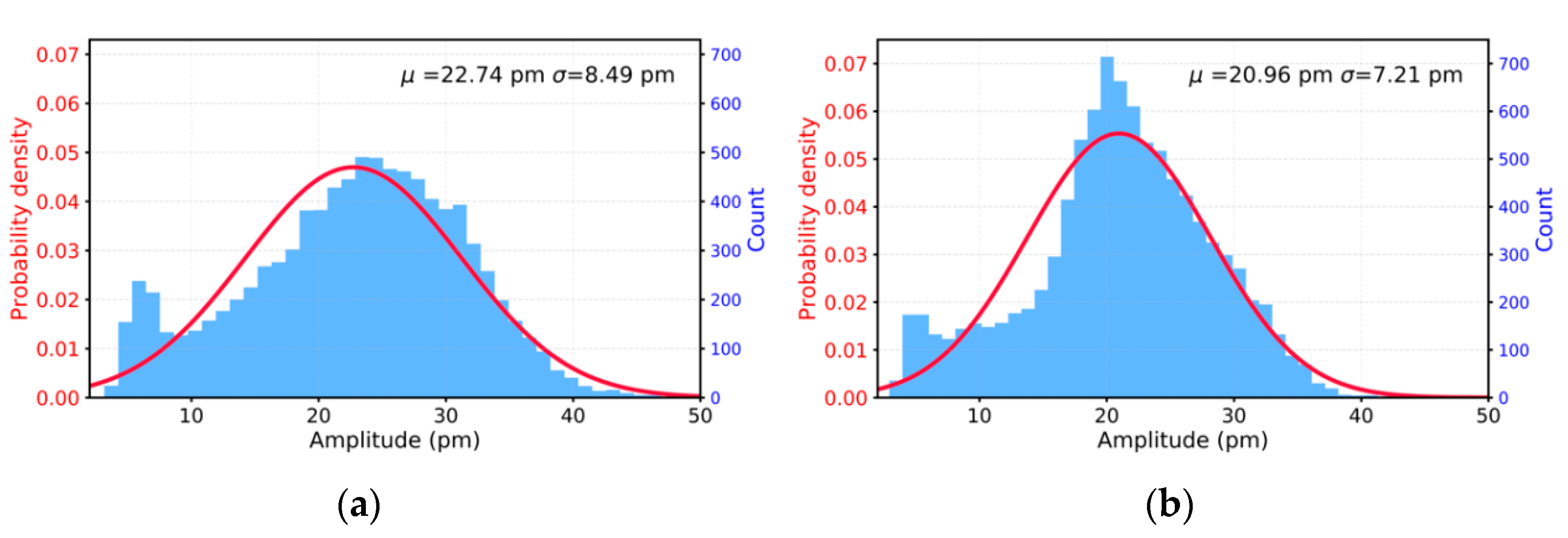
Piezoelectric Characterization

To explore the effectiveness of the gravure printing method compared to the ALD process for growing ZnO seed layers on the flexible substrates, we carried out PFM measurements on the ZnO (ALD)/ITO/Si and as-printed (not sintered) ZnO seed layer/ITO/PET samples. The PFM is a widely used tool to study the polarity and the piezo-response properties of piezoelectric thin films and NWs. In this work, the PFM was carried out using the DataCube mode to study the polarities on the top surface of ZnO NWs by recording the phase signals. The d 33 piezoelectric coefficients were computed by analysing the piezoelectric amplitudes as presented in Figure 5a–f.
Figure 5a,b show the topography in an area of 2 × 2 µm2 in a top-view of ZnO NWs grown on ITO/Si and ITO/PET structures. At first view, we can see good uniformity and an excellent hexagonal shape for the ZnO NWs as per the SEM results (Figure 4). Besides, they have the same correlation regarding their diameter (between 53 and 210 nm) and roughness parameters at the top end of ZnO (e.g., root mean square (Rq) values are approximately 120 nm). Figure 5c,d show the PFM amplitudes for both samples when an AC drive voltage of 5 V was applied. The mean amplitude values (µ) were very similar (22.74 ± 8.49 pm and 20.96 ± 7.21 pm, as shown in Figure 6, for ITO/Si and ITO/PET, respectively) according to the Gaussian fitting function for piezoelectric amplitude distribution at the top surface of ZnO NWs. Based on these results, we estimated the effective piezoelectric coefficients ( d 33 e f f ) to be 4.6 and 4.1 pm/V for the ZnO NWs grown on ITO/Si and ITO/PET, respectively. It is important to highlight that both samples presented almost the same d 33 e f f values and they were inside the range of the previously reported experimental results of 2–12 pm/V [104,105,106,107,108].
On the other hand, the PFM measurements also provided results concerning the piezoelectric phase as depicted in Figure 5e,f. Both results show a single-phase value of around 75° (see Figure S3) throughout the top surface of ZnO NWs, thus demonstrating the Zn surface polarity of the crystal structure [64]. Obtaining a homogeneous surface polarity is very important at a device level, i.e., where NWs are typically integrated and placed between electrodes [33]. If the NWs had shown negative and positive phase values in their top surface, the induced negative and positive electrical charges would have cancelled out, thus reducing the overall piezoelectric response at the device level.

4. Conclusions

In summary, our experimental results show that gravure printing is a promising low-temperature ZnO seeding method, especially from the perspective of fabricating flexible piezoelectric devices. Study of the printed seed layer morphology revealed that the nanoparticulate allowed a better growth of vertical ZnO NWs by CBD with respect to the sintered one because the high-energy NPs provided a higher number of nucleation sites. To explain the observed results, a possible reorientation mechanism of the ZnO nanoparticle seeds was also proposed. PFM measurements of the NWs revealed (i) a Zn-phase polarity with a very good homogeneity, which is essential to obtaining globally optimal piezoelectric performance when integrated in devices, and (ii) an estimated piezoelectric coefficient close to 4 pm/V, which is comparable to the NWs grown on Si/ITO substrate.
The mobility and flexibility of the whole structure, provided by the use of flexible ZnO NWs, is expected to have a good impact on the device’s mechanical performance and durability.
This work shows the way towards the fabrication of flexible piezoelectric transducers based on ZnO nanowires. Fabrication is completely carried out by solution processes at a low temperature.

Supplementary Materials

The following are available online at https://www.mdpi.com/article/10.3390/nano11061430/s1, Figure S1: sweep of drive frequency value of AC bias signal for PFM amplitude and phase values in different ranges of frequency; Figure S2: single frame of (a) amplitude and (b) phase measurement and average value of 20 frames of (c) amplitude and (d) phase; Figure S3: piezoelectric phase distribution value of ZnO NWs grown on (a) ZnO (ALD)/ITO/Si and (b) as-printed (non-sintered) ZnO seed layer/ITO/PET substrates. The red curve is the fitting curve using Gaussian mixture models, Figure S4: height distribution of the top surface of (a) ITO over PET, (b) ITO over Si, and (c) ZnO seed layer (deposited by ALD) over ITO/Si to extract the roughness parameters by AFM; Figure S5: diameter distribution of ZnO NWs grown on (a) ZnO (ALD)/ITO/Si and (b) as-printed (non-sintered) ZnO seed layer/ITO/PET substrates. The red curve is the Gaussian fitting function; Figure S6: SEM image of the cross-section of the ZnO NWs grown on (a) ITO/Si substrate and (b) ITO/PET substrate; Figure S7: Raman spectra of ZnO seed layer films deposited onto aluminium by gravure printing measured before and after 4 h of sintering; Table S1: arithmetical mean deviation values (Ra) and root squared values (Rq) measured for the different substrates and manufactured ZnO seed layers; Table S2: comparison table of ZnO NWs grown by chemical bath deposition (CBD) from recent articles; Table S3: assignments for the Raman bands marked in Figure S2 to specific vibrations for ZnO structures.

Author Contributions

Conceptualization, G.A.; G.N.; G.S.; methodology, A.J.L.G.; V.D.; G.S.; M.M.; software, A.J.L.G.; validation, A.J.L.G.; V.D.; G.A.; G.S.; M.M.; formal analysis, A.J.L.G.; investigation, A.J.L.G.; V.D.; M.P.; G.S.; M.M.; F.L.; F.V.; resources, X.M.; G.S.; M.M.; F.L.; F.V.; data curation, A.J.L.G.; writing—original draft preparation, A.J.L.G.; G.A.; V.D.; M.P.; G.S.; M.M.; F.L.; F.V.; G.N.; writing—review and editing, G.A.; M.P.; X.M.; G.S.; M.M.; F.L.; F.V.; G.N.; visualization, A.J.L.G.; V.D.; supervision, G.A.; project administration, G.A.; funding acquisition, G.A.; G.N. All authors have read and agreed to the published version of the manuscript.

Funding

This work has received funding from project PULSE-COM of the European Union’s Horizon 2020 research and innovation program under grant agreement No. 863227.

Data Availability Statement

The data are available upon request from the corresponding authors.

Acknowledgments

This work has been performed with the help of the “Plateforme Technologique Amont” from Grenoble.

Conflicts of Interest

The authors declare no conflict of interest.

References

  1. Aliqué, M.; Simão, C.D.; Murillo, G.; Moya, A. Fully-Printed Piezoelectric Devices for Flexible Electronics Applications. Adv. Mater. Technol. 2021, 6, 2001020. [Google Scholar] [CrossRef]
  2. Martins, P.; Lopes, A.C.; Lanceros-Mendez, S. Electroactive phases of poly(vinylidene fluoride): Determination, processing and applications. Prog. Polym. Sci. 2014, 39, 683–706. [Google Scholar] [CrossRef]
  3. Bhavanasi, V.; Kumar, V.; Parida, K.; Wang, J.; Lee, P.S. Enhanced Piezoelectric Energy Harvesting Performance of Flexible PVDF-TrFE Bilayer Films with Graphene Oxide. ACS Appl. Mater. Interfaces 2016, 8, 521–529. [Google Scholar] [CrossRef]
  4. Wu, Y.; Qu, J.; Daoud, W.A.; Wang, L.; Qi, T. Flexible composite-nanofiber based piezo-triboelectric nanogenerators for wearable electronics. J. Mater. Chem. A 2019, 7, 13347–13355. [Google Scholar] [CrossRef]
  5. Costa, P.; Nunes-Pereira, J.; Pereira, N.; Castro, N.; Gonçalves, S.; Lanceros-Mendez, S. Recent Progress on Piezoelectric, Pyroelectric, and Magnetoelectric Polymer-Based Energy-Harvesting Devices. Energy Technol. 2019, 7, 1–19. [Google Scholar] [CrossRef]
  6. Gupta, S.; Bhunia, R.; Fatma, B.; Maurya, D.; Singh, D.; Gupta, R.; Priya, S.; Gupta, R.K.; Garg, A. Multifunctional and Flexible Polymeric Nanocomposite Films with Improved Ferroelectric and Piezoelectric Properties for Energy Generation Devices. ACS Appl. Mater. Interfaces 2019, 2, 6364–6374. [Google Scholar] [CrossRef]
  7. Kang, H.B.; Han, C.S.; Pyun, J.C.; Ryu, W.H.; Kang, C.Y.; Cho, Y.S. (Na,K)NbO3 nanoparticle-embedded piezoelectric nanofiber composites for flexible nanogenerators. Compos. Sci. Technol. 2015, 111, 1–8. [Google Scholar] [CrossRef]
  8. Hwang, G.T.; Park, H.; Lee, J.H.; Oh, S.; Park, K.I.; Byun, M.; Park, H.; Ahn, G.; Jeong, C.K.; No, K.; et al. Self-powered cardiac pacemaker enabled by flexible single crystalline PMN-PT piezoelectric energy harvester. Adv. Mater. 2014, 26, 4880–4887. [Google Scholar] [CrossRef]
  9. Dudem, B.; Kim, D.H.; Bharat, L.K.; Yu, J.S. Highly-flexible piezoelectric nanogenerators with silver nanowires and barium titanate embedded composite films for mechanical energy harvesting. Appl. Energy 2018, 230, 865–874. [Google Scholar] [CrossRef]
  10. Rovisco, A.; dos Santos, A.; Cramer, T.; Martins, J.; Branquinho, R.; Águas, H.; Fraboni, B.; Fortunato, E.; Martins, R.; Igreja, R. Piezoelectricity Enhancement of Nanogenerators Based on PDMS and ZnSnO3 Nanowires through Microstructuration. ACS Appl. Mater. Interfaces 2020, 12, 18421–18430. [Google Scholar] [CrossRef]
  11. Queraltó, A.; Frohnhoven, R.; Mathur, S.; Gómez, A. Intrinsic piezoelectric characterization of BiFeO3 nanofibers and its implications for energy harvesting. Appl. Surf. Sci. 2020, 509, 144760–144767. [Google Scholar] [CrossRef]
  12. Yang, D.; Qiu, Y.; Jiang, Q.; Guo, Z.; Song, W.; Xu, J.; Zong, Y.; Feng, Q.; Sun, X. Patterned growth of ZnO nanowires on flexible substrates for enhanced performance of flexible piezoelectric nanogenerators. Appl. Phys. Lett. 2017, 110, 63901–63905. [Google Scholar] [CrossRef]
  13. Panth, M.; Cook, B.; Alamri, M.; Ewing, D.; Wilson, A.; Wu, J.Z. Flexible zinc oxide nanowire array/graphene nanohybrid for high-sensitivity strain detection. ACS Omega 2020, 5, 27359–27367. [Google Scholar] [CrossRef] [PubMed]
  14. Wei, H.; Wang, H.; Xia, Y.; Cui, D.; Shi, Y.; Dong, M.; Liu, C.; Ding, T.; Zhang, J.; Ma, Y. An overview of lead-free piezoelectric materials and devices. J. Mater. Chem. C 2018, 6, 12446–12467. [Google Scholar] [CrossRef]
  15. Hughes, W.L.; Wang, Z.L. Controlled synthesis and manipulation of ZnO nanorings and nanobows. Appl. Phys. Lett. 2005, 86, 43106. [Google Scholar] [CrossRef]
  16. Espinosa, H.D.; Bernal, R.A.; Minary-Jolandan, M. A review of mechanical and electromechanical properties of piezoelectric nanowires. Adv. Mater. 2012, 24, 4656–4675. [Google Scholar] [CrossRef] [PubMed]
  17. Jing, G.; Zhang, X.; Yu, D. Effect of surface morphology on the mechanical properties of ZnO nanowires. Appl. Phys. A 2010, 100, 473–478. [Google Scholar] [CrossRef]
  18. Chen, C.Q.; Shi, Y.; Zhang, Y.S.; Zhu, J.; Yan, Y.J. Size dependence of Young’s modulus in ZnO nanowires. Phys. Rev. Lett. 2006, 96, 75505–75508. [Google Scholar] [CrossRef]
  19. Soomro, M.Y.; Hussain, I.; Bano, N.; Broitman, E.; Nur, O.; Willander, M. Nanoscale elastic modulus of single horizontal ZnO nanorod using nanoindentation experiment. Nanoscale Res. Lett. 2012, 7, 1–5. [Google Scholar] [CrossRef] [Green Version]
  20. Agrawal, R.; Espinosa, H.D. Giant piezoelectric size effects in zinc oxide and gallium nitride nanowires. A first principles investigation. Nano Lett. 2011, 11, 786–790. [Google Scholar] [CrossRef] [PubMed]
  21. Tao, R.; Mouis, M.; Ardila, G. Unveiling the influence of surface fermi level pinning on the piezoelectric response of semiconducting nanowires. Adv. Electron. Mater. 2018, 4, 1700299. [Google Scholar] [CrossRef]
  22. Hussain, S.; Liu, T.; Aslam, N.; Kashif, M.; Cao, S.; Rashad, M.; Zhang, Y.; Zeng, W.; Javed, M.S. Polymer-assisted co-axial multi-layered circular ZnO nanodisks. Mater. Lett. 2015, 152, 260–263. [Google Scholar] [CrossRef]
  23. Hussain, S.; Liu, T.; Aslam, N.; Zhao, S.; Li, T.; Hou, D.; Zeng, W. Assembly of bulbous ZnO nanorods to bulbous nanoflowers and their high selectivity towards formaldehyde. J. Mater. Sci. Mater. Electron. 2016, 27, 4966–4971. [Google Scholar] [CrossRef]
  24. Hussain, S.; Yang, X.; Aslam, M.K.; Shaheen, A.; Javed, M.S.; Aslam, N.; Aslam, B.; Liu, G.; Qiao, G. Robust TiN nanoparticles polysulfide anchor for Li–S storage and diffusion pathways using first principle calculations. Chem. Eng. J. 2020, 391, 123595. [Google Scholar] [CrossRef]
  25. Hussain, S.; Khan, A.J.; Arshad, M.; Javed, M.S.; Ahmad, A.; Shah, S.S.A.; Khan, M.R.; Akram, S.; Zulfiqar; Ali, S.; et al. Charge storage in binder-free 2D-hexagonal CoMoO4 nanosheets as a redox active material for pseudocapacitors. Ceram. Int. 2021, 47, 8659–8667. [Google Scholar] [CrossRef]
  26. Hussain, S.; Hassan, M.; Javed, M.S.; Shaheen, A.; Ahmad Shah, S.S.; Nazir, M.T.; Najam, T.; Khan, A.J.; Zhang, X.; Liu, G. Distinctive flower-like CoNi2S4 nanoneedle arrays (CNS–NAs) for superior supercapacitor electrode performances. Ceram. Int. 2020, 46, 25942–25948. [Google Scholar] [CrossRef]
  27. Wang, Z.L.; Song, J. Piezoelectric Nanogenerators Based on Zinc Oxide Nanowire. Science 2006, 312, 242–246. [Google Scholar] [CrossRef] [PubMed]
  28. Yang, R.; Qin, Y.; Li, C.; Zhu, G.; Wang, Z.L. Converting biomechanical energy into electricity by a muscle-movement-driven nanogenerator. Nano Lett. 2009, 9, 1201–1205. [Google Scholar] [CrossRef]
  29. Yim, M.; Jeon, B.; Yoon, G. Fabrication of tandem-type vertically integrated nanogenerator by in-situ deposition of AlN/ZnO films. J. Semicond. Technol. Sci. 2019, 19, 233–238. [Google Scholar] [CrossRef]
  30. Dahiya, A.S.; Morini, F.; Boubenia, S.; Nadaud, K.; Alquier, D.; Poulin-Vittrant, G. Organic/Inorganic Hybrid Stretchable Piezoelectric Nanogenerators for Self-Powered Wearable Electronics. Adv. Mater. Technol. 2018, 3, 1–11. [Google Scholar] [CrossRef] [Green Version]
  31. Lee, S.; Bae, S.H.; Lin, L.; Yang, Y.; Park, C.; Kim, S.W.; Cha, S.N.; Kim, H.; Park, Y.J.; Wang, Z.L. Super-flexible nanogenerator for energy harvesting from gentle wind and as an active deformation sensor. Adv. Funct. Mater. 2013, 23, 2445–2449. [Google Scholar] [CrossRef] [Green Version]
  32. Yu, A.; Li, H.; Tang, H.; Liu, T.; Jiang, P.; Wang, Z.L. Vertically integrated nanogenerator based on ZnO nanowire arrays. Phys. Status Solidi Rapid Res. Lett. 2011, 5, 162–164. [Google Scholar] [CrossRef]
  33. Tao, R.; Parmar, M.; Ardila, G.; Oliveira, P.; Marques, D.; Montès, L.; Mouis, M. Performance of ZnO based piezo-generators under controlled compression. Semicond. Sci. Technol. 2017, 32, 064003. [Google Scholar] [CrossRef]
  34. Hu, Y.; Lin, L.; Zhang, Y.; Wang, Z.L. Replacing a battery by a nanogenerator with 20 v output. Adv. Mater. 2012, 24, 110–114. [Google Scholar] [CrossRef]
  35. Zhu, G.; Wang, A.C.; Liu, Y.; Zhou, Y.; Wang, Z.L. Functional electrical stimulation by nanogenerator with 58 V output voltage. Nano Lett. 2012, 12, 3086–3090. [Google Scholar] [CrossRef] [PubMed] [Green Version]
  36. Yuan, H.; Lei, T.; Qin, Y.; Yang, R. Flexible electronic skins based on piezoelectric nanogenerators and piezotronics. Nano Energy 2019, 59, 84–90. [Google Scholar] [CrossRef]
  37. He, H.; Fu, Y.; Zang, W.; Wang, Q.; Xing, L.; Zhang, Y.; Xue, X. A flexible self-powered T-ZnO/PVDF/fabric electronic-skin with multi-functions of tactile-perception, atmosphere-detection and self-clean. Nano Energy 2017, 31, 37–48. [Google Scholar] [CrossRef]
  38. Baxter, J.B.; Schmuttenmaer, C.A. Conductivity of ZnO nanowires, nanoparticles, and thin films using time-resolved terahertz spectroscopy. J. Phys. Chem. B 2006, 110, 25229–25239. [Google Scholar] [CrossRef]
  39. Villafuerte, J.; Donatini, F.; Kioseoglou, J.; Sarigiannidou, E.; Chaix-Pluchery, O.; Pernot, J.; Consonni, V. Zinc Vacancy–Hydrogen Complexes as Major Defects in ZnO Nanowires Grown by Chemical Bath Deposition. J. Phys. Chem. C 2020, 124, 16652–16662. [Google Scholar] [CrossRef]
  40. Sugunan, A.; Warad, H.C.; Boman, M.; Dutta, J. Zinc oxide nanowires in chemical bath on seeded substrates: Role of hexamine. J. Sol-Gel Sci. Technol. 2006, 39, 49–56. [Google Scholar] [CrossRef]
  41. Chelu, M.; Stroescu, H.; Anastasescu, M.; Calderon-Moreno, J.M.; Preda, S.; Stoica, M.; Fogarassy, Z.; Petrik, P.; Gheorghe, M.; Parvulescu, C. High-quality PMMA/ZnO NWs piezoelectric coating on rigid and flexible metallic substrates. Appl. Surf. Sci. 2020, 529, 147135–147144. [Google Scholar] [CrossRef]
  42. Yang, W.; Wang, Y.; Hou, Z.; Li, C. A facile hot-pressing process for fabricating flexible top electrodes of piezoelectric ZnO nanowire nanogenerators. Nanotechnology 2019, 30, 505402–505407. [Google Scholar] [CrossRef] [PubMed]
  43. Deng, W.; Jin, L.; Zhang, B.; Chen, Y.; Mao, L.; Zhang, H.; Yang, W. A flexible field-limited ordered ZnO nanorod-based self-powered tactile sensor array for electronic skin. Nanoscale 2016, 8, 16302–16306. [Google Scholar] [CrossRef] [PubMed]
  44. Yilmaz, P.; Greenwood, P.; Meroni, S.; Troughton, J.; Novák, P.; Li, X.; Watson, T.; Briscoe, J. Self-adhesive electrode applied to ZnO nanorod-based piezoelectric nanogenerators. Smart Mater. Struct. 2019, 28, 105040. [Google Scholar] [CrossRef] [Green Version]
  45. Zhang, Y.; Liu, C.; Liu, J.; Xiong, J.; Liu, J.; Zhang, K.; Liu, Y.; Peng, M.; Yu, A.; Zhang, A. Lattice strain induced remarkable enhancement in piezoelectric performance of ZnO-based flexible nanogenerators. ACS Appl. Mater. Interfaces 2016, 8, 1381–1387. [Google Scholar] [CrossRef] [PubMed]
  46. Wojnarowicz, J.; Chudoba, T.; Lojkowski, W. A Review of Microwave Synthesis of Zinc Oxide Nanomaterials: Reactants, Process Parameters and Morphoslogies. Nanomaterials 2020, 10, 1086. [Google Scholar] [CrossRef]
  47. Noack, V.; Eychmüller, A. Annealing of nanometer-sized zinc oxide particles. Chem. Mater. 2002, 14, 1411–1417. [Google Scholar] [CrossRef]
  48. Mosalagae, K.; Murape, D.M.; Lepodise, L.M. Effects of growth conditions on properties of CBD synthesized ZnO nanorods grown on ultrasonic spray pyrolysis deposited ZnO seed layers. Heliyon 2020, 6, e04458–e04467. [Google Scholar] [CrossRef]
  49. Chang, S.-Y.; Yang, N.-H.; Huang, Y.-C.; Lin, S.-J.; Kattamis, T.Z.; Liu, C.-Y. Spontaneous growth of one-dimensional nanostructures from films in ambient atmosphere at room temperature: ZnO and TiO2. J. Mater. Chem. 2011, 21, 4264–4271. [Google Scholar] [CrossRef]
  50. Peiris, T.A.N.; Alessa, H.; Sagu, J.S.; Bhatti, I.A.; Isherwood, P.; Wijayantha, K.G.U. Effect of ZnO seed layer thickness on hierarchical ZnO nanorod growth on flexible substrates for application in dye-sensitised solar cells. J. Nanoparticle Res. 2013, 15, 2115–2124. [Google Scholar] [CrossRef]
  51. Burke-Govey, C.P.; Plank, N.O.V. Review of hydrothermal ZnO nanowires: Toward FET applications. J. Vac. Sci. Technol. B Nanotechnol. Microelectron. Mater. Process. Meas. Phenom. 2013, 31, F101–F106. [Google Scholar] [CrossRef]
  52. Wei, P.; Zhu, D.; Huang, S.; Zhou, W.; Luo, F. Effects of the annealing temperature and atmosphere on the microstructures and dielectric properties of ZnO/Al2O3 composite coatings. Appl. Surf. Sci. 2013, 285, 577–582. [Google Scholar] [CrossRef]
  53. Ranjan, P.; Suematsu, H.; Chakravarthy, S.R.; Jayaganthan, R.; Sarathi, R. Thermodynamic analysis of ZnO nanoparticle formation by wire explosion process and characterization. Ceram. Int. 2017, 43, 6709–6720. [Google Scholar] [CrossRef]
  54. Wu, W. Inorganic nanomaterials for printed electronics: A review. Nanoscale 2017, 9, 7342–7372. [Google Scholar] [CrossRef]
  55. Abbel, R.; Galagan, Y.; Groen, P. Roll-to-Roll Fabrication of Solution Processed Electronics. Adv. Eng. Mater. 2018, 20, 1701190–1701219. [Google Scholar] [CrossRef] [Green Version]
  56. Khan, S.; Lorenzelli, L.; Dahiya, R.S. Technologies for printing sensors and electronics over large flexible substrates: A review. IEEE Sens. J. 2014, 15, 3164–3185. [Google Scholar] [CrossRef]
  57. Arrabito, G.; Aleeva, Y.; Pezzilli, R.; Ferrara, V.; Medaglia, P.G.; Pignataro, B.; Prestopino, G. Printing ZnO Inks: From Principles to Devices. Crystals 2020, 10, 449. [Google Scholar] [CrossRef]
  58. Søndergaard, R.R.; Hösel, M.; Krebs, F.C. Roll-to-Roll fabrication of large area functional organic materials. J. Polym. Sci. Part. B Polym. Phys. 2013, 51, 16–34. [Google Scholar] [CrossRef]
  59. Krebs, F.C. Fabrication and processing of polymer solar cells: A review of printing and coating techniques. Sol. Energy Mater. Sol. Cells 2009, 93, 394–412. [Google Scholar] [CrossRef]
  60. Sico, G.; Montanino, M.; Prontera, C.T.; Del Mauro, A.D.G.; Minarini, C. Gravure printing for thin film ceramics manufacturing from nanoparticles. Ceram. Int. 2018, 44, 19526–19534. [Google Scholar] [CrossRef]
  61. Sico, G.; Montanino, M.; Ventre, M.; Mollo, V.; Prontera, C.T.; Minarini, C.; Magnani, G. Pressureless sintering of ZnO thin film on plastic substrate via vapor annealing process at near-room temperature. Scr. Mater. 2019, 164, 48–51. [Google Scholar] [CrossRef]
  62. Choi, Y.; Kim, G.H.; Jeong, W.H.; Kim, H.J.; Chin, B.D.; Yu, J.-W. Characteristics of gravure printed InGaZnO thin films as an active channel layer in thin film transistors. Thin Solid Film. 2010, 518, 6249–6252. [Google Scholar] [CrossRef]
  63. Kim, S.; Seol, D.; Lu, X.; Alexe, M.; Kim, Y. Electrostatic-free piezoresponse force microscopy. Sci. Rep. 2017, 7, 1–8. [Google Scholar] [CrossRef] [PubMed]
  64. Bui, Q.C.; Ardila, G.; Sarigiannidou, E.; Roussel, H.; Jiménez, C.; Chaix-Pluchery, O.; Guerfi, Y.; Bassani, F.; Donatini, F.; Mescot, X.; et al. Morphology Transition of ZnO from Thin Film to Nanowires on Silicon and its Correlated Enhanced Zinc Polarity Uniformity and Piezoelectric Responses. ACS Appl. Mater. Interfaces 2020, 12, 29583–29593. [Google Scholar] [CrossRef]
  65. Kumar, Y.; Rana, A.K.; Bhojane, P.; Pusty, M.; Bagwe, V.; Sen, S.; Shirage, P.M. Controlling of ZnO nanostructures by solute concentration and its effect on growth, structural and optical properties. Mater. Res. Express 2015, 2, 105017–105027. [Google Scholar] [CrossRef] [Green Version]
  66. Guillemin, S.; Consonni, V.; Appert, E.; Puyoo, E.; Rapenne, L.; Roussel, H. Critical nucleation effects on the structural relationship between ZnO seed layer and nanowires. J. Phys. Chem. C 2012, 116, 25106–25111. [Google Scholar] [CrossRef]
  67. Guillemin, S.; Rapenne, L.; Roussel, H.; Sarigiannidou, E.; Brémond, G.; Consonni, V. Formation mechanisms of ZnO nanowires: The crucial role of crystal orientation and polarity. J. Phys. Chem. C 2013, 117, 20738–20745. [Google Scholar] [CrossRef]
  68. Abdulrahman, A.F.; Ahmed, S.M.; Ahmed, N.M.; Almessiere, M.A. Enhancement of ZnO Nanorods Properties Using Modified Chemical Bath Deposition Method: Effect of Precursor Concentration. Crystals 2020, 10, 386. [Google Scholar] [CrossRef]
  69. Zuniga-Perez, J.; Consonni, V.; Lymperakis, L.; Kong, X.; Trampert, A.; Fernandez-Garrido, S.; Brandt, O.; Renevier, H.; Keller, S.; Hestroffer, K. Polarity in GaN and ZnO: Theory, measurement, growth, and devices. Appl. Phys. Rev. 2016, 3, 41303–41402. [Google Scholar] [CrossRef] [Green Version]
  70. Marks, L.D.; Peng, L. Nanoparticle shape, thermodynamics and kinetics. J. Phys. Condens. Matter 2016, 28, 53001–53048. [Google Scholar] [CrossRef]
  71. Levitas, V.I.; Samani, K. Size and mechanics effects in surface-induced melting of nanoparticles. Nat. Commun. 2011, 2, 1–6. [Google Scholar] [CrossRef] [Green Version]
  72. Vollath, D.; Fischer, F.D.; Holec, D. Surface energy of nanoparticles–influence of particle size and structure. Beilstein J. Nanotechnol. 2018, 9, 2265–2276. [Google Scholar] [CrossRef]
  73. Biener, J.; Wittstock, A.; Baumann, T.F.; Weissmüller, J.; Bäumer, M.; Hamza, A.V. Surface chemistry in nanoscale materials. Materials 2009, 2, 2404–2428. [Google Scholar] [CrossRef]
  74. Choudhary, K.; Biacchi, A.J.; Ghosh, S.; Hale, L.; Walker, A.R.H.; Tavazza, F. High-throughput assessment of vacancy formation and surface energies of materials using classical force-fields. J. Phys. Condens. Matter 2018, 30, 395901. [Google Scholar] [CrossRef] [PubMed] [Green Version]
  75. Meulenkamp, E.A. Synthesis and growth of ZnO nanoparticles. J. Phys. Chem. B 1998, 102, 5566–5572. [Google Scholar] [CrossRef]
  76. Przybyszewska, M.; Krzywania, A.; Zaborski, M.; Szynkowska, M.I. Surface properties of zinc oxide nanoparticles studied by inverse gas chromatography. J. Chromatogr. A 2009, 1216, 5284–5291. [Google Scholar] [CrossRef] [PubMed]
  77. Lu, H.M.; Jiang, Q. Size-dependent surface energies of nanocrystals. J. Phys. Chem. B 2004, 108, 5617–5619. [Google Scholar] [CrossRef]
  78. He, H.; Cao, J.; Duan, N. Defects and their behaviors in mineral dissolution under water environment: A review. Sci. Total Environ. 2019, 651, 2208–2217. [Google Scholar] [CrossRef] [PubMed]
  79. Ching, K.-L.; Li, G.; Ho, Y.-L.; Kwok, H.-S. The role of polarity and surface energy in the growth mechanism of ZnO from nanorods to nanotubes. CrystEngComm 2016, 18, 779–786. [Google Scholar] [CrossRef]
  80. Kralchevsky, P.A.; Nagayama, K. Capillary forces between colloidal particles. Langmuir 1994, 10, 23–36. [Google Scholar] [CrossRef]
  81. Mudunkotuwa, I.A.; Grassian, V.H. The devil is in the details (or the surface): Impact of surface structure and surface energetics on understanding the behavior of nanomaterials in the environment. J. Environ. Monit. 2011, 13, 1135–1144. [Google Scholar] [CrossRef] [PubMed]
  82. Zhang, P.; Xu, F.; Navrotsky, A.; Lee, J.S.; Kim, S.; Liu, J. Surface enthalpies of nanophase ZnO with different morphologies. Chem. Mater. 2007, 19, 5687–5693. [Google Scholar] [CrossRef]
  83. Tang, C.; Spencer, M.J.S.; Barnard, A.S. Activity of ZnO polar surfaces: An insight from surface energies. Phys. Chem. Chem. Phys. 2014, 16, 22139–22144. [Google Scholar] [CrossRef] [PubMed]
  84. Connolly, B.M.; Greer, H.F.; Zhou, W. Formation Mechanisms of ZnO Spherulites and Derivatives. Cryst. Growth Des. 2018, 19, 249–257. [Google Scholar] [CrossRef] [Green Version]
  85. Demes, T.; Ternon, C.; Riassetto, D.; Stambouli, V.; Langlet, M. Comprehensive study of hydrothermally grown ZnO nanowires. J. Mater. Sci. 2016, 51, 10652–10661. [Google Scholar] [CrossRef]
  86. Cossuet, T.; Roussel, H.; Chauveau, J.-M.; Chaix-Pluchery, O.; Thomassin, J.-L.; Appert, E.; Consonni, V. Well-ordered ZnO nanowires with controllable inclination on semipolar ZnO surfaces by chemical bath deposition. Nanotechnology 2018, 29, 475601–475612. [Google Scholar] [CrossRef] [PubMed]
  87. Theissmann, R.; Fendrich, M.; Zinetullin, R.; Guenther, G.; Schierning, G.; Wolf, D.E. Crystallographic reorientation and nanoparticle coalescence. Phys. Rev. B 2008, 78, 205413–205421. [Google Scholar] [CrossRef]
  88. Ali, A.; Ambreen, S.; Javed, R.; Tabassum, S.; Ul Haq, I.; Zia, M. ZnO nanostructure fabrication in different solvents transforms physio-chemical, biological and photodegradable properties. Mater. Sci. Eng. C 2017, 74, 137–145. [Google Scholar] [CrossRef]
  89. Castro, R.H.R.; Gouvêa, D. Sintering and nanostability: The thermodynamic perspective. J. Am. Ceram. Soc. 2016, 99, 1105–1121. [Google Scholar] [CrossRef]
  90. German, R.M. Sintering trajectories: Description on how density, surface area, and grain size change. JOM 2016, 68, 878–884. [Google Scholar] [CrossRef] [Green Version]
  91. Rohrer, G.S. Grain boundary energy anisotropy: A review. J. Mater. Sci. 2011, 46, 5881–5895. [Google Scholar] [CrossRef] [Green Version]
  92. Lee, J.; Wiederhorn, S.M. Effects of polarity on grain-boundary migration in ZnO. J. Am. Ceram. Soc. 2004, 87, 1319–1323. [Google Scholar] [CrossRef]
  93. German, R.M. Coarsening in sintering: Grain shape distribution, grain size distribution, and grain growth kinetics in solid-pore systems. Crit. Rev. Solid State Mater. Sci. 2010, 35, 263–305. [Google Scholar] [CrossRef]
  94. Sui, M.; Pandey, P.; Li, M.-Y.; Zhang, Q.; Kunwar, S.; Lee, J. Tuning the configuration of Au nanostructures: From vermiform-like, rod-like, triangular, hexagonal, to polyhedral nanostructures on c-plane GaN. J. Mater. Sci. 2017, 52, 391–407. [Google Scholar] [CrossRef]
  95. Kuang, Q.; Wang, X.; Jiang, Z.; Xie, Z.; Zheng, L. High-energy-surface engineered metal oxide micro- and nanocrystallites and their applications. Acc. Chem. Res. 2014, 47, 308–318. [Google Scholar] [CrossRef]
  96. Syrrokostas, G.; Govatsi, K.; Yannopoulos, S.N. High-Quality, Reproducible ZnO Nanowire Arrays Obtained by a Multiparameter Optimization of Chemical Bath Deposition Growth. Cryst. Growth Des. 2016, 16, 2140–2150. [Google Scholar] [CrossRef]
  97. Hussain, S.; Liu, T.; Kashif, M.; Miao, B.; He, J.; Zeng, W.; Zhang, Y.; Hashim, U.; Pan, F. Surfactant dependent growth of twinned ZnO nanodisks. Mater. Lett. 2014, 118, 165–168. [Google Scholar] [CrossRef]
  98. Qiu, J.; Weng, B.; Zhao, L.; Chang, C.; Shi, Z.; Li, X.; Kim, H.K.; Hwang, Y.H. Synthesis and characterization of flower-like bundles of ZnO nanosheets by a surfactant-free hydrothermal process. J. Nanomater. 2014, 2014. [Google Scholar] [CrossRef] [Green Version]
  99. Ashfold, M.N.R.; Doherty, R.P.; Ndifor-Angwafor, N.G.; Riley, D.J.; Sun, Y. The kinetics of the hydrothermal growth of ZnO nanostructures. Thin Solid Film. 2007, 515, 8679–8683. [Google Scholar] [CrossRef]
  100. Strom, J.G., Jr.; Jun, H.W. Kinetics of hydrolysis of methenamine. J. Pharm. Sci. 1980, 69, 1261–1263. [Google Scholar] [CrossRef] [PubMed]
  101. Govender, K.; Boyle, D.S.; Kenway, P.B.; O’Brien, P. Understanding the factors that govern the deposition and morphology of thin films of ZnO from aqueous solution. J. Mater. Chem. 2004, 14, 2575–2591. [Google Scholar] [CrossRef]
  102. Ruiz-Rojas, C.A.; Aguilar-Frutis, M.; Ramos-Brito, F.; Garduno-Wilches, I.A.; Narro-Ríos, J.; Lartundo-Rojas, L.; Alarcón-Flores, G. Synthesis, characterization, and temperature-dependent electronic properties of ZnO nanorods using CBD techniques. J. Mater. Sci. Mater. Electron. 2021, 1–14. [Google Scholar] [CrossRef]
  103. Parize, R.; Garnier, J.; Chaix-Pluchery, O.; Verrier, C.; Appert, E.; Consonni, V. Effects of Hexamethylenetetramine on the Nucleation and Radial Growth of ZnO Nanowires by Chemical Bath Deposition. J. Phys. Chem. C 2016, 120, 5242–5250. [Google Scholar] [CrossRef]
  104. Tamvakos, D.; Lepadatu, S.; Antohe, V.-A.; Tamvakos, A.; Weaver, P.M.; Piraux, L.; Cain, M.G.; Pullini, D. Piezoelectric properties of template-free electrochemically grown ZnO nanorod arrays. Appl. Surf. Sci. 2015, 356, 1214–1220. [Google Scholar] [CrossRef]
  105. Broitman, E.; Soomro, M.Y.; Lu, J.; Willander, M.; Hultman, L. Nanoscale piezoelectric response of ZnO nanowires measured using a nanoindentation technique. Phys. Chem. Chem. Phys. 2013, 15, 11113–11118. [Google Scholar] [CrossRef] [PubMed] [Green Version]
  106. Fan, H.J.; Lee, W.; Hauschild, R.; Alexe, M.; Le Rhun, G.; Scholz, R.; Dadgar, A.; Nielsch, K.; Kalt, H.; Krost, A. Template-assisted large-scale ordered arrays of ZnO pillars for optical and piezoelectric applications. Small 2006, 2, 561–568. [Google Scholar] [CrossRef] [PubMed]
  107. Scrymgeour, D.A.; Sounart, T.L.; Simmons, N.C.; Hsu, J.W.P. Polarity and piezoelectric response of solution grown zinc oxide nanocrystals on silver. J. Appl. Phys. 2007, 101, 14316–14321. [Google Scholar] [CrossRef]
  108. Cavallini, D.; Fortunato, M.; De Bellis, G.; Sarto, M.S. PFM Characterization of Piezoelectric PVDF/ZnONanorod thin films. In Proceedings of the 2018 IEEE 18th International Conference on Nanotechnology (IEEE-NANO), Cork, Ireland, 23–26 July 2018; IEEE: Piscataway, NJ, USA, 2018; pp. 1–3. [Google Scholar]
Figure 1. Fabrication process of ZnO seed layers by gravure printing and subsequent NW growth. The gravure printing process can be divided in the following steps: (a) inking, doctoring, and transfer; (b) spreading; (c) drying; (d) production of the final solid thin film. (e) The final growth of ZnO NWs is performed via low-temperature CBD.
Nanomaterials 11 01430 g001
Figure 2. (a) SEM image; (a’) magnified SEM image; (b) AFM phase image; (b’) magnified AFM phase image of the as-printed (non-sintered) ZnO seed layer.
Nanomaterials 11 01430 g002
Figure 3. (a) SEM image; (a’) magnified SEM image; (b) AFM phase image; (b’) magnified AFM phase image of the sintered printed ZnO seed layer obtained after 4 h of treatment.
Nanomaterials 11 01430 g003
Figure 4. SEM images of the ZnO NWs grown on a (a) ZnO (ALD)/ITO/Si substrate; (a’) magnified image; (b) as-printed (non-sintered) ZnO seed layer/ITO/PET; (b’) magnified image; (c) sintered printed ZnO seed layer/ITO/PET; (c’) magnified image.
Nanomaterials 11 01430 g004
Figure 5. PFM images of the (a,b) topography, (c,d) amplitude, and (e,f) phase of the ZnO NW growth on ZnO (ALD)/ITO/Si (images lined up above) and as-printed (not sintered) ZnO seed layer/ITO/PET substrates (images lined up below).
Nanomaterials 11 01430 g005
Figure 6. Piezoelectric amplitude histograms of ZnO NW growth on (a) ZnO (ALD)/ITO/Si and (b) as-printed (not sintered) ZnO seed layer/ITO/PET substrates. The red curve is the Gaussian fitting function.
Nanomaterials 11 01430 g006
Publisher’s Note: MDPI stays neutral with regard to jurisdictional claims in published maps and institutional affiliations.

