
Temperature Effect of van der Waals Epitaxial GaN Films on Pulse-Laser-Deposited 2D MoS2 Layer


Abstract
1. Introduction
2. Materials and Methods
3. Results and Discussion
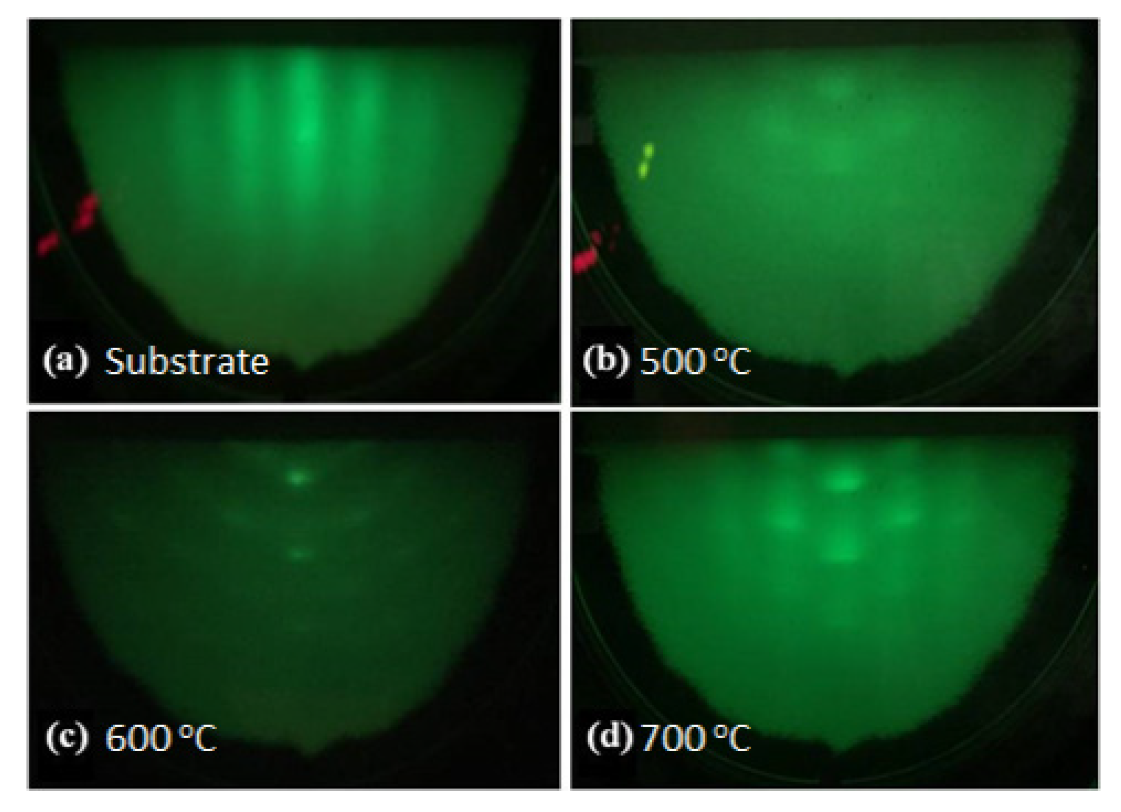
3.1. In Situ Characterizations by Reflection High Energy Electron Diffraction
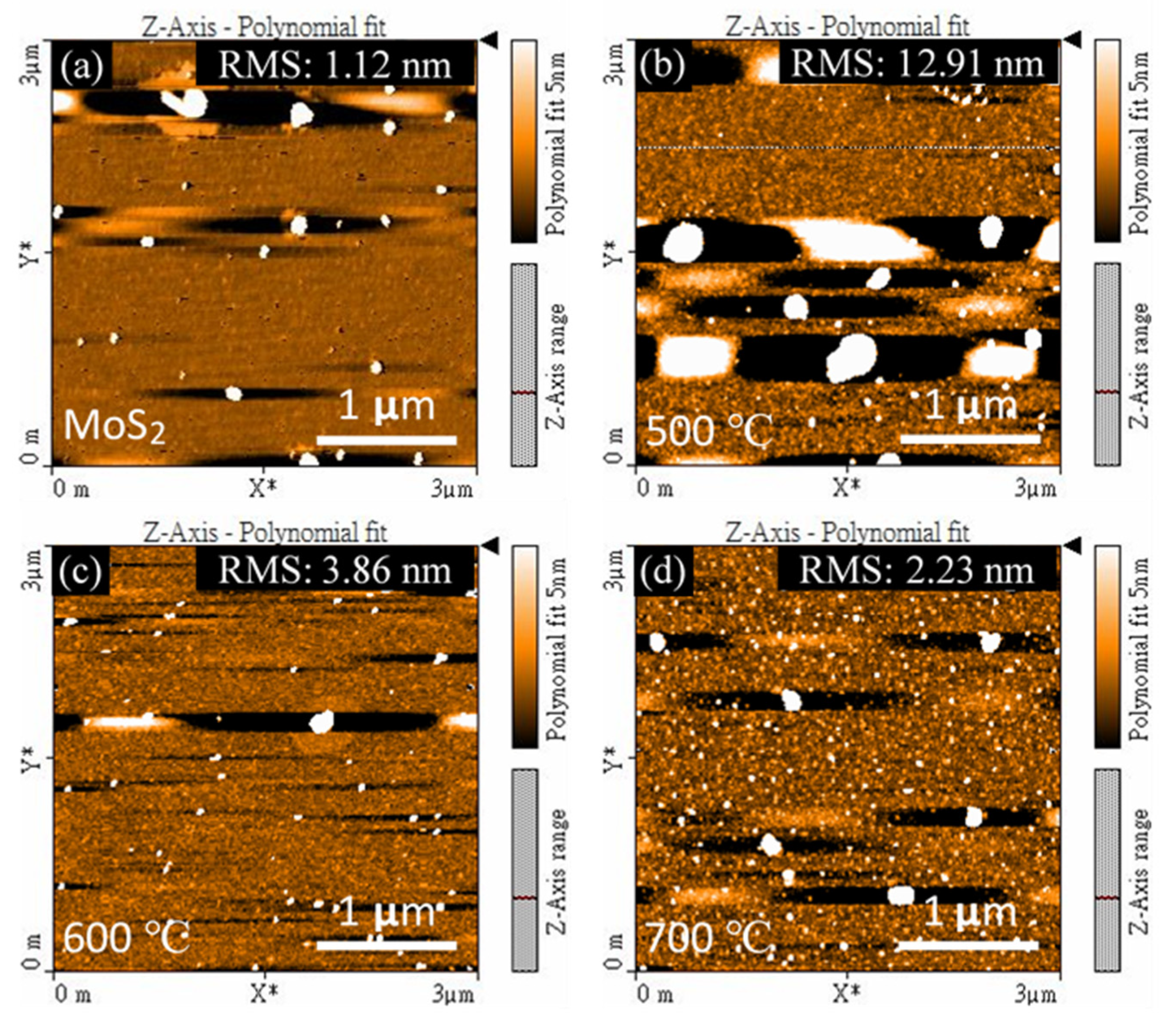
3.2. The Observation of Atomic Force Microscopy
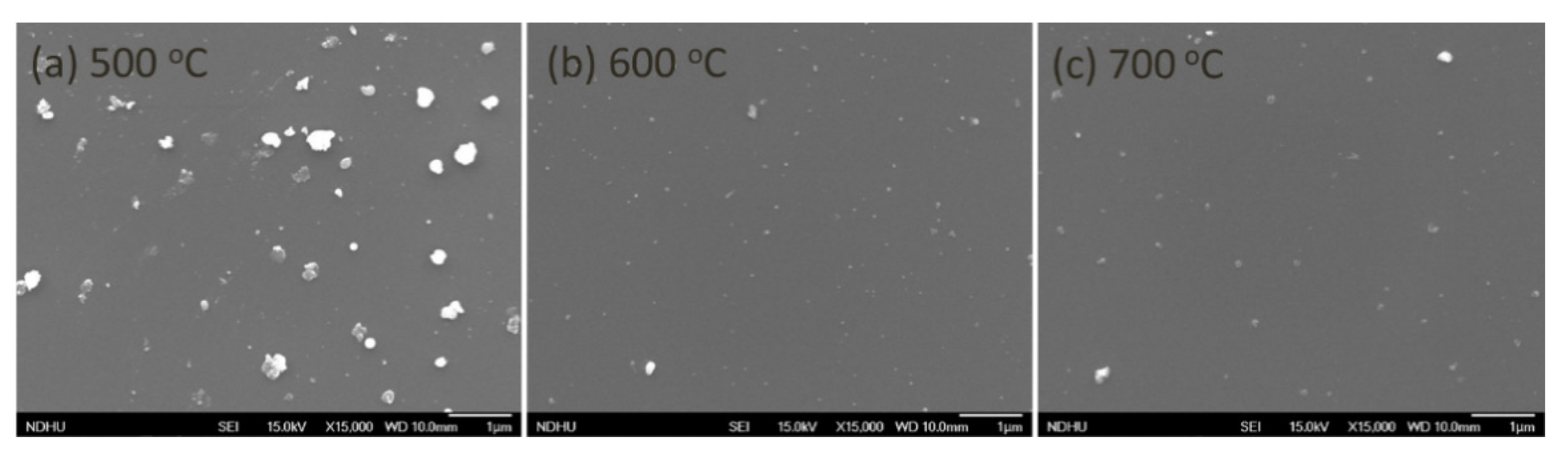
3.3. The Observation of Scanning Electron Microscopy
3.4. The Analysis of X-ray Photoelectron Spectroscopy
3.5. The Analysis of Raman Spectroscopy
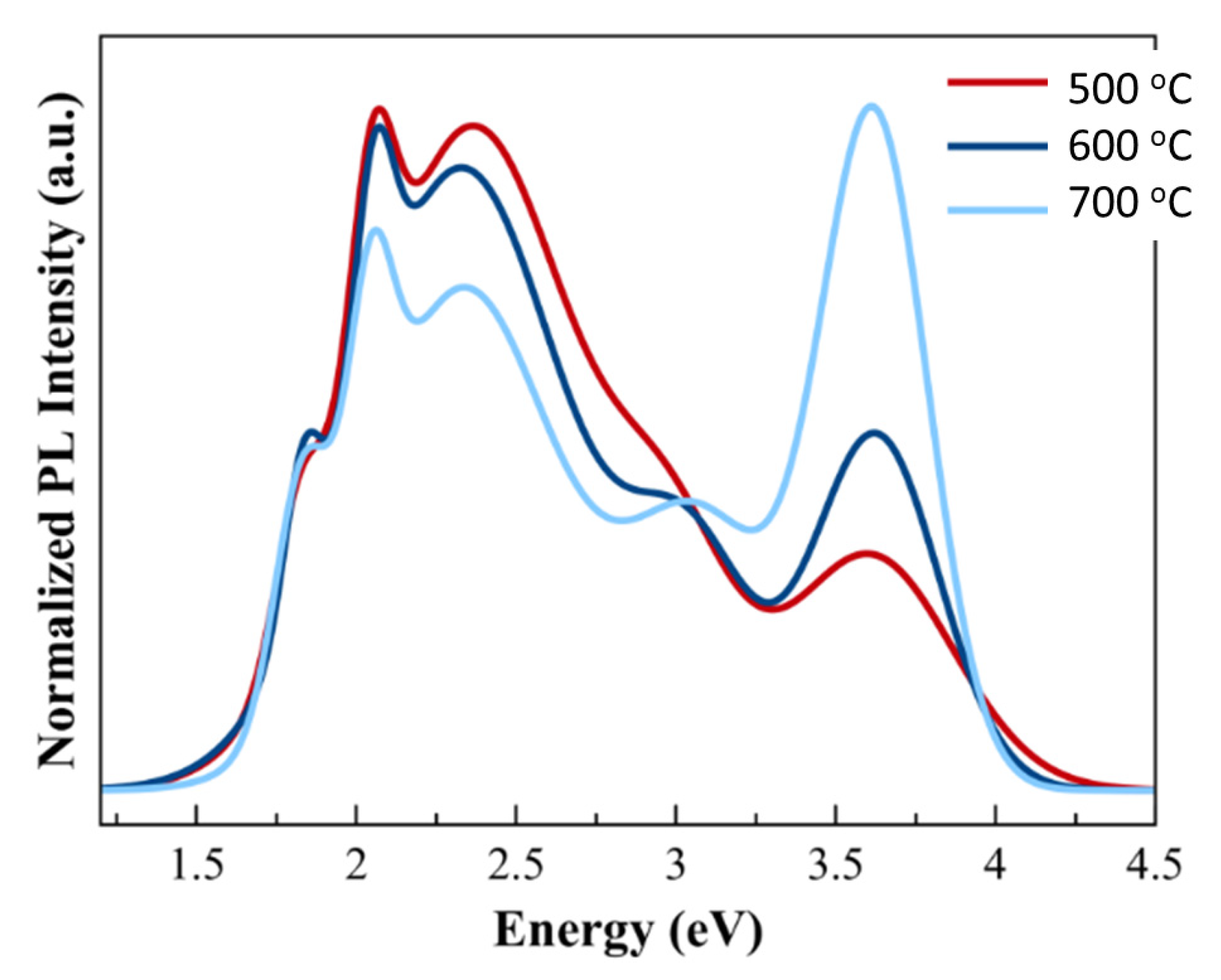
3.6. The Analysis of Photoluminescence Spectroscopy
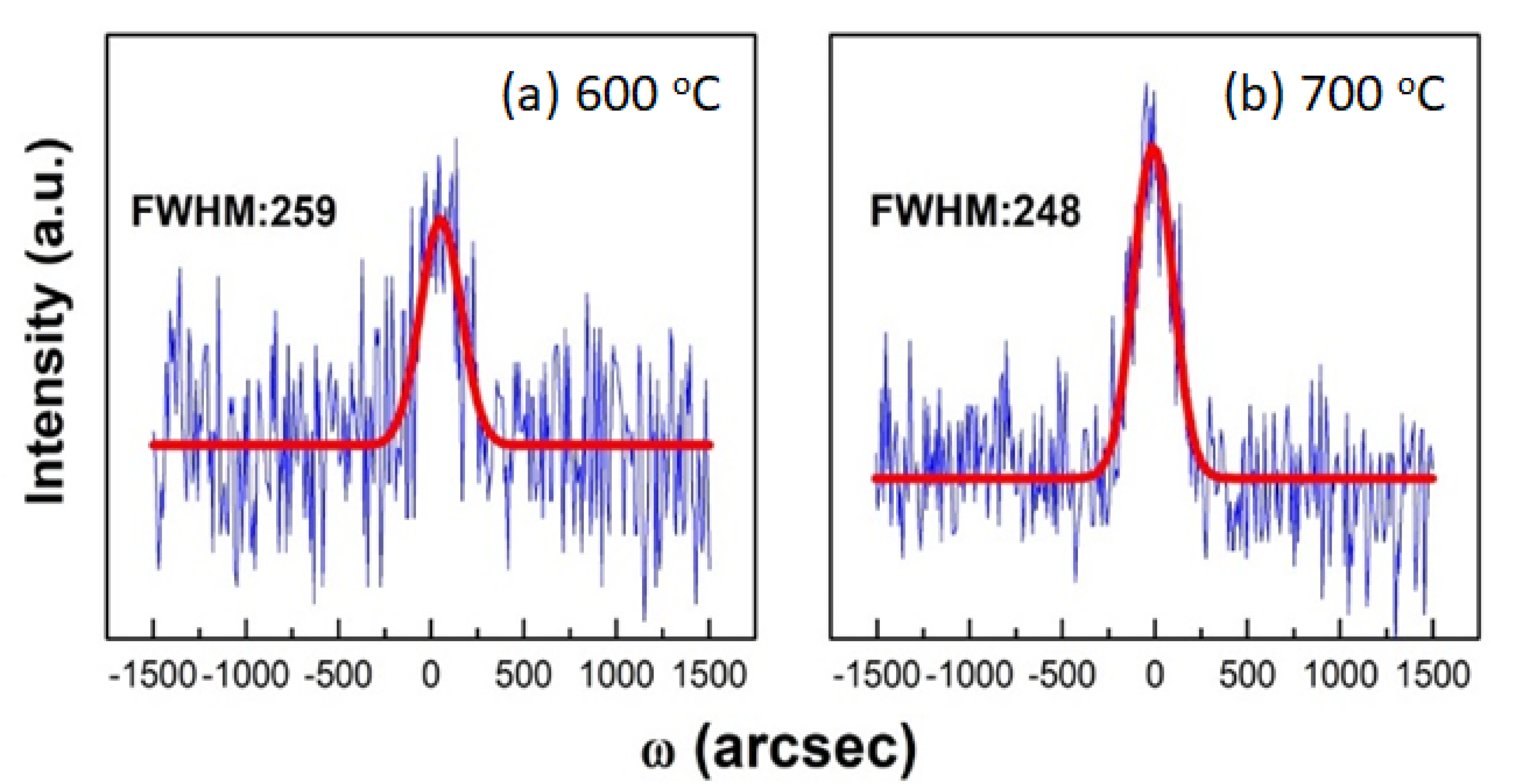
3.7. The Analysis of X-ray Diffraction
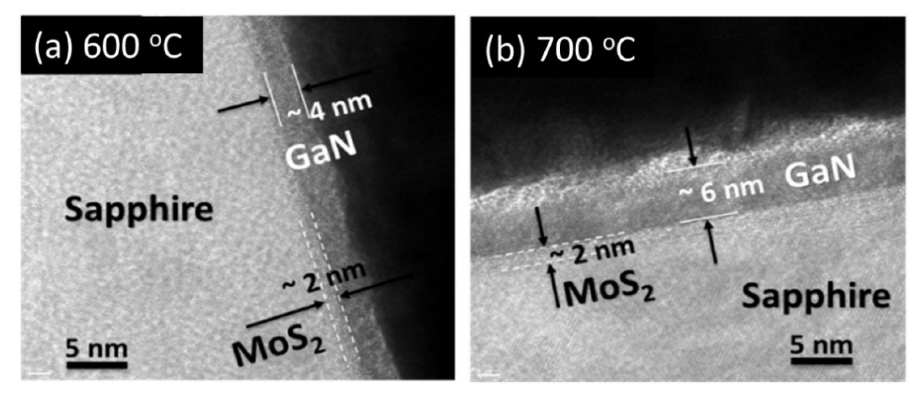
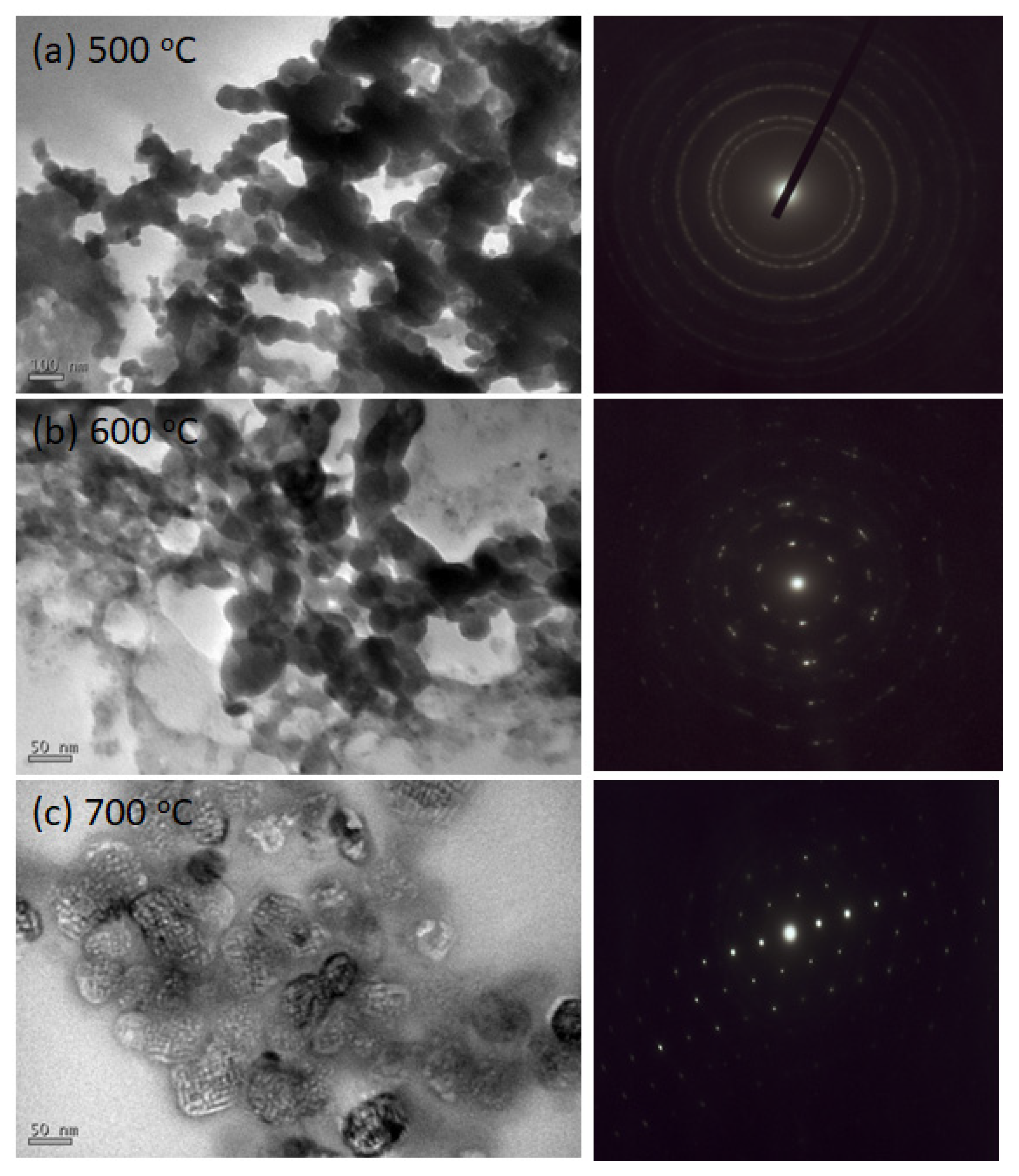
3.8. The Observation of Transmission Electron Microscopy
4. Conclusions
Author Contributions
Funding
Data Availability Statement
Acknowledgments
Conflicts of Interest
References
- Liao, W.; Huang, Y.; Wang, H.; Zhang, H. Van der Waals heterostructures for optoelectronics: Progress and prospects. Appl. Mater. Today. 2019, 16, 435–455. [Google Scholar] [CrossRef]
- Chung, K.; Yoo, H.; Hyun, J.K.; Oh, H.; Tchoe, Y.; Lee, K.; Baek, H.; Kim, M.; Yi, G.C. Flexible GaN light-emitting diodes using GaN microdisks epitaxial laterally overgrown on graphene dots. Adv. Mater. 2016, 28, 7688–7694. [Google Scholar] [CrossRef]
- Zhu, D.; Wallis, D.J.; Humphreys, C.J. Prospects of III-nitride optoelectronics grown on Si. Rep. Prog. Phys. 2013, 76, 106501. [Google Scholar] [CrossRef] [PubMed]
- Wu, J. When group-III nitrides go infrared: New properties and perspectives. J. Appl. Phys. 2009, 106, 011101. [Google Scholar] [CrossRef]
- Chen, Y.; Liu, J.; Liu, K.; Si, J.; Ding, Y.; Li, L.; Lv, T.; Liu, J.; Fu, L. GaN in different dimensionalities: Properties, synthesis, and applications. Mater. Sci. Eng. R Reports. 2019, 138, 60–84. [Google Scholar] [CrossRef]
- Hashizume, T.; Nishiguchi, K.; Kaneki, S.; Kuzmik, J.; Yatabe, Z. State of the art on gate insulation and surface passivation for GaN-based power HEMTs. Mater. Sci. Semicond. Process. 2018, 78, 85–95. [Google Scholar] [CrossRef]
- Goswami, L.; Pandey, R.; Gupta, G. Epitaxial growth of GaN nanostructure by PA-MBE for UV detection application. Appl. Surf. Sci. 2018, 449, 186–192. [Google Scholar] [CrossRef]
- Wang, Q.; Gao, X.; Xu, Y.; Leng, J. Carrier localization in strong phase-separated InGaN/GaN multiple-quantum-well dual-wavelength LEDs. J. Alloys Compd. 2017, 726, 460–465. [Google Scholar] [CrossRef]
- Liu, L.; Edgar, J.H. Substrates for gallium nitride epitaxy. Mater. Sci. Eng. R Rep. 2002, 37, 61–127. [Google Scholar] [CrossRef]
- Yang, Z.P.; Tsou, T.H.; Lee, C.Y.; Kan, K.Y.; Yu, I.S. Effects of substrate and annealing on GaN films grown by plasma-assisted molecular beam epitaxy. Surf. Coatings Technol. 2017, 320, 548–553. [Google Scholar] [CrossRef]
- Utama, M.I.B.; Zhang, Q.; Zhang, J.; Yuan, Y.; Bellarre, F.J.; Arbiol, J.; Xiong, Q. Recent developments and future directions in the growth of nanostructures by van der Waals epitaxy. Nanoscale 2013, 5, 3570–3588. [Google Scholar] [CrossRef]
- Lin, Z.; Zhao, Y.; Zhou, C.; Zhong, R.; Wang, X.; Tsang, Y.S.; Chai, Y. Controllable growth of large-size crystalline MoS2 and resist-free transfer assisted with a Cu thin film. Sci. Rep. 2015, 5, 1–10. [Google Scholar] [CrossRef]
- Yu, H.; Liao, M.; Zhao, W.; Liu, G.; Zhou, X.J.; Wei, Z.; Xu, X.; Liu, K.; Hu, Z.; Deng, K.; et al. Wafer-scale growth and transfer of highly-oriented monolayer MoS2 continuous films. ACS Nano 2017, 11, 12001–12007. [Google Scholar] [CrossRef] [PubMed]
- Alaskar, Y.; Arafin, S.; Wickramaratne, D.; Zurbuchen, M.A.; He, L.; Mckay, J.; Lin, Q.; Goorsky, M.S.; Lake, R.K.; Wang, K.L. Towards van der Waals epitaxial growth of GaAs on Si using a graphene buffer layer. Adv. Funct. Mater. 2014, 24, 6629–6638. [Google Scholar] [CrossRef]
- Li, T.; Liu, C.; Zhang, Z.; Yu, B.; Dong, H.; Jia, W.; Jia, Z.; Yu, C.; Gan, L.; Xu, B. GaN epitaxial layers grown on multilayer graphene by MOCVD. AIP Adv. 2018, 8, 045105. [Google Scholar] [CrossRef]
- Ajayan, P.; Kim, P.; Banerjee, K. Two-dimensional van der Waals materials. Phys. Today 2016, 69, 38–44. [Google Scholar] [CrossRef]
- Zhang, X.; Meng, F.; Christianson, J.R.; Arroyo-Torres, C.; Lukowski, M.A.; Liang, D.; Schmidt, J.R.; Jin, S. Vertical heterostructures of layered metal chalcogenides by van der Waals epitaxy. Nano Lett. 2014, 14, 3047–3054. [Google Scholar] [CrossRef] [PubMed]
- Tangi, M.; Mishra, P.; Ng, T.K.; Hedhili, M.N.; Janjua, B.; Alias, M.S.; Anjum, D.H.; Tseng, C.C.; Shi, Y.; Joyce, S.Y.; et al. Determination of band offsets at GaN/single-layer MoS2 heterojunction. Appl. Phys. Lett. 2016, 109, 032104. [Google Scholar] [CrossRef]
- Gupta, P.; Rahman, A.A.; Subramanian, S.; Gupta, S.; Thamizhavel, A.; Orlava, T.; Rouvimou, S.; Vishwanath, S.; Protasenko, V.; Laskar, M.R.; et al. Layered transition metal dichalcogenides: Promising near-lattice-matched substrates for GaN growth. Sci. Rep. 2016, 6, 23708. [Google Scholar] [CrossRef]
- Susanto, I.; Tsai, C.Y.; Rahmiati, T.; Ho, Y.T.; Tsai, P.Y.; Yu, S. The influence of 2D MoS2 layers on the growth of GaN films by plasma-assisted molecular beam epitaxy. Appl. Surf. Sci. 2019, 496, 143616. [Google Scholar] [CrossRef]
- Yang, Z.; Hao, J. Progress in pulsed laser deposited two-dimensional layered materials for device applications. J. Mater. Chem. C 2016, 4, 8859–8878. [Google Scholar] [CrossRef]
- Koblmüller, G.; Lang, J.R.; Young, E.C.; Speck, J.S. Handbook of Crystal Growth: Thin Films and Epitaxy, 2nd ed.; Kuech, T.K., Ed.; Elsevier: Amsterdam, The Netherlands, 2015; pp. 705–754. [Google Scholar]
- Fuke, S.; Sasaki, T.; Takahasi, M.; Hibino, H. In-situ X-ray diffraction analysis of GaN growth on graphene-covered amorphous substrates. Jpn. J. Appl. Phys. 2020, 59, 070902. [Google Scholar] [CrossRef]
- Aggarwal, N.; Krishna, S.T.C.; Goswami, L.; Mishra, M.; Gupta, G.; Maurya, K.K.; Singh, S.; Dilawa, N.; Kaur, M. Extenuation of stress and defects in GaN films grown on a metal–organic chemical vapor deposition-GaN/c-sapphire substrate by plasma-assisted molecular beam epitaxy. Cryst. Growth Des. 2015, 15, 2144–2150. [Google Scholar] [CrossRef]
- Krishna, S.; Aggarwal, N.; Mishra, M.; Maurya, K.K.; Singh, S.; Dilawar, N.; Najarajan, S.; Gupta, G. Correlation of growth temperature with stress, defect states and electronic structure in an epitaxial GaN film grown on c-sapphire via plasma MBE. Phys. Chem. Chem. Phys. 2016, 18, 8005–8014. [Google Scholar] [CrossRef] [PubMed]
- Susanto, I.; Kan, K.Y.; Yu, I.S. Temperature effects for GaN films grown on 4H-SiC substrate with 4° miscutting orientation by plasma-assisted molecular beam epitaxy. J. Alloys Compd. 2017, 723, 21–29. [Google Scholar] [CrossRef]
- Ho, Y.T.; Ma, C.H.; Luong, T.T.; Wei, L.L.; Yen, T.C.; Hsu, W.T.; Chang, W.H.; Chu, Y.C.; Tu, Y.Y.; Pande, K.P.; et al. Layered MoS2 grown on c -sapphire by pulsed laser deposition. Phys. Status Solidi Rapid Res. Lett. 2015, 9, 187–191. [Google Scholar] [CrossRef]
- Kumar, P.; Kuyyalil, J.; Shivaprasad, S.M. Ga induced superstructures as templates for lattice matched hetroepitaxial growth of GaN on Si (111) substrate. Appl. Phys. Lett. 2010, 97, 28–31. [Google Scholar] [CrossRef]
- Susanto, I.; Tsou, T.H.; Yang, Z.P.; Lee, C.Y.; Li, H.; Yu, I.S. Effects of N/Ga flux ratio on GaN films grown on 4H-SiC substrate with 4° miscutting orientation by plasma-assisted molecular beam epitaxy. J. Alloys Compd. 2017, 710, 800–808. [Google Scholar] [CrossRef]
- Mishra, M.; Krishna, T.C.S.; Aggarwal, N.; Kaur, M.; Singh, S.; Gupta, G. Pit assisted oxygen chemisorption on GaN surfaces. Phys. Chem. Chem. Phys. 2015, 17, 15201–15208. [Google Scholar] [CrossRef]
- Kushvaha, S.S.; Kumar, M.S.; Shukla, A.; Yadav, B.S.; Singh, D.K.; Jewariya, M.J.; Ragam, S.; Maurya, K.K. Structural, optical and electronic properties of homoepitaxial GaN nanowalls grown on GaN template by laser molecular beam epitaxy. RSC Adv. 2015, 5, 87818–87830. [Google Scholar] [CrossRef]
- Thakur, V.; Shivaprasad, S.M. Electronic structure of GaN nanowall network analysed by XPS. Appl. Surf. Sci. 2015, 327, 389–393. [Google Scholar] [CrossRef]
- Chakraborty, B.; Bera, A.; Muthu, D.V.S.; Bhowmick, S.; Waghmare, U.V.; Sood, A.K. Symmetry-dependent phonon renormalization in monolayer MoS2 transistor. Phys. Rev. B Condens. Matter Mater. Phys. 2012, 85, 2–5. [Google Scholar] [CrossRef]
- Hushur, A.; Manghnani, M.H.; Narayan, J. Raman studies of GaN/sapphire thin film heterostructures. J. Appl. Phys. 2009, 106, 054317. [Google Scholar] [CrossRef]
- Grieshaber, W.; Schubert, E.F.; Goepfert, I.D.; Karlicek, R.F.; Schuman, M.J.; Tran, C. Competition between band gap and yellow luminescence in GaN and its relevance for optoelectronic devices. J. Appl. Phys. 1996, 80, 4615–4620. [Google Scholar] [CrossRef]
- Eeshchikov, M.A.; Morkoc, H. Luminescence properties of defect in GaN. J. Appl. Phys. 2005, 97, 061301. [Google Scholar] [CrossRef]
- Julkarnain, M.; Kamata, N.; Fukuda, T.; Arakawa, Y. Yellow luminescence band in undoped GaN revealed by two-wavelength excited photoluminescence. Opt. Mater. 2016, 60, 481–486. [Google Scholar] [CrossRef]
- Tuan, T.T.A.; Kuo, D.H.; Li, C.C.; Li, G.Z. Effect of temperature dependence on electrical characterization of p-n GaN diode fabricated by RF magnetron sputtering. Mater. Sci. Appl. 2015, 6, 809–817. [Google Scholar]


| Sample | Substrate | Thermal Cleaning | Pre-Nitridation Treatment | GaN Growth Temperature | GaN Growth Time |
|---|---|---|---|---|---|
| T1 | MoS2/c-sapphire | 600 °C | 600 °C | 500 °C | 20 min |
| T2 | 40 min | 20 min | 600 °C | ||
| T3 | 700 °C |
| Sample | Peak Position (eV) | Percentage (%) | RGa-Ga/Ga-N (%) | ||||
|---|---|---|---|---|---|---|---|
| Ga-N | Ga-Ga | O-O | Ga-N | Ga-Ga | O-O | ||
| T1 | 19.91 | 18.08 | 22.98 | 83.3 | 11.1 | 5.6 | 13 |
| T2 | 20.03 | 18.23 | 23.48 | 81.4 | 8.9 | 9.7 | 10 |
| T3 | 19.89 | 18.28 | 23.15 | 92.7 | 5.1 | 2.2 | 5 |
Publisher’s Note: MDPI stays neutral with regard to jurisdictional claims in published maps and institutional affiliations. |
© 2021 by the authors. Licensee MDPI, Basel, Switzerland. This article is an open access article distributed under the terms and conditions of the Creative Commons Attribution (CC BY) license (https://creativecommons.org/licenses/by/4.0/).
Share and Cite
Susanto, I.; Tsai, C.-Y.; Ho, Y.-T.; Tsai, P.-Y.; Yu, I.-S. Temperature Effect of van der Waals Epitaxial GaN Films on Pulse-Laser-Deposited 2D MoS2 Layer. Nanomaterials 2021, 11, 1406. https://doi.org/10.3390/nano11061406
Susanto I, Tsai C-Y, Ho Y-T, Tsai P-Y, Yu I-S. Temperature Effect of van der Waals Epitaxial GaN Films on Pulse-Laser-Deposited 2D MoS2 Layer. Nanomaterials. 2021; 11(6):1406. https://doi.org/10.3390/nano11061406
Chicago/Turabian StyleSusanto, Iwan, Chi-Yu Tsai, Yen-Teng Ho, Ping-Yu Tsai, and Ing-Song Yu. 2021. "Temperature Effect of van der Waals Epitaxial GaN Films on Pulse-Laser-Deposited 2D MoS2 Layer" Nanomaterials 11, no. 6: 1406. https://doi.org/10.3390/nano11061406
APA StyleSusanto, I., Tsai, C.-Y., Ho, Y.-T., Tsai, P.-Y., & Yu, I.-S. (2021). Temperature Effect of van der Waals Epitaxial GaN Films on Pulse-Laser-Deposited 2D MoS2 Layer. Nanomaterials, 11(6), 1406. https://doi.org/10.3390/nano11061406