
Improved Device Distribution in High-Performance SiNx Resistive Random Access Memory via Arsenic Ion Implantation


Abstract
1. Introduction
2. Materials and Methods
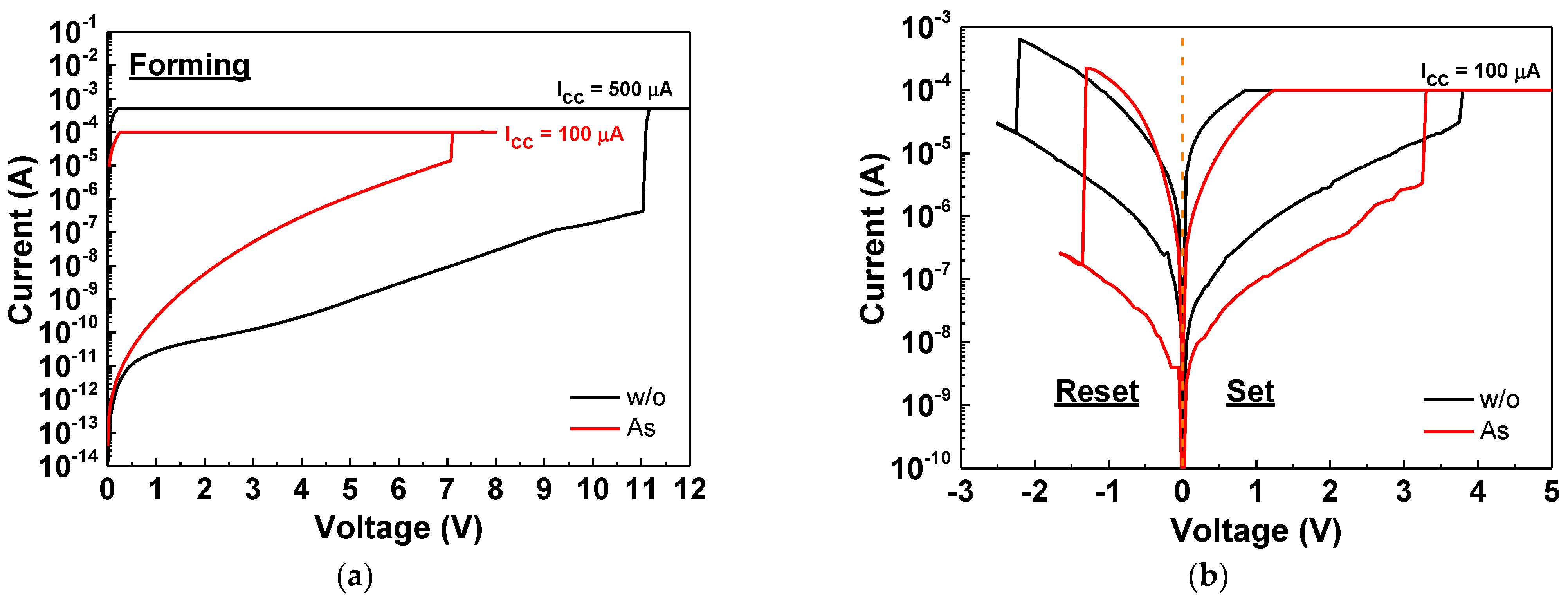
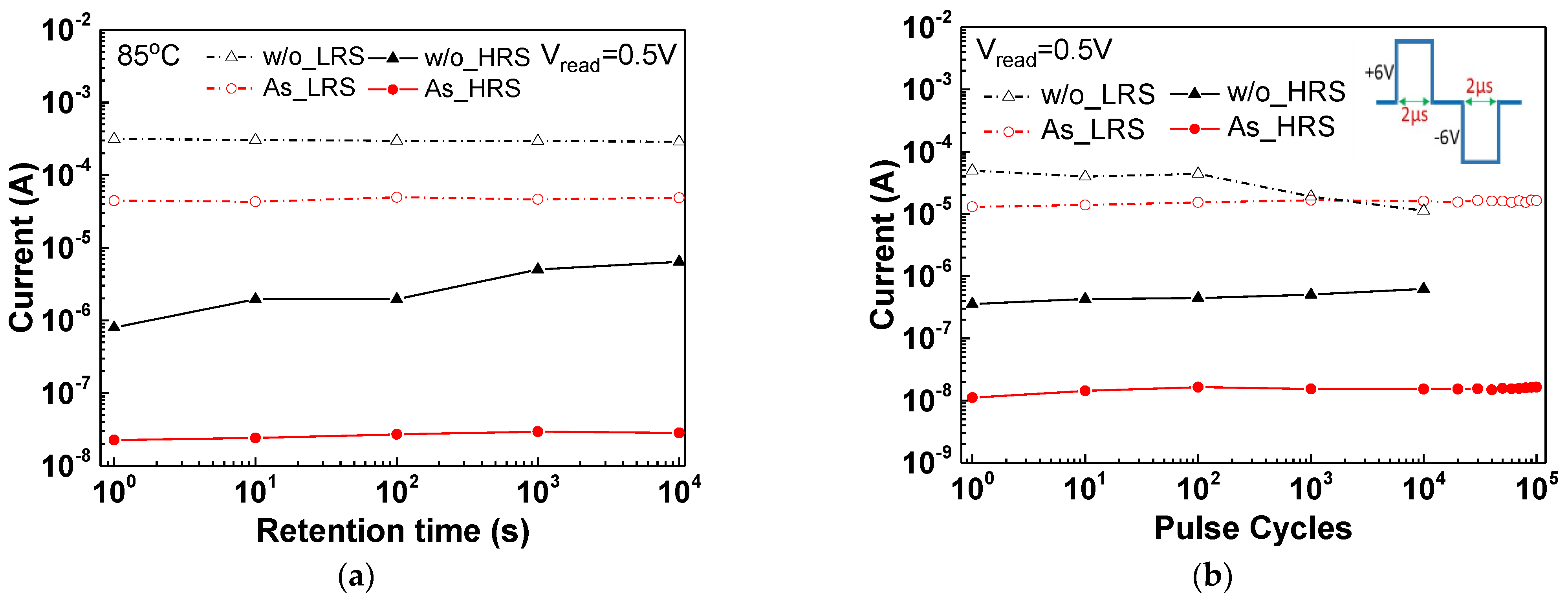
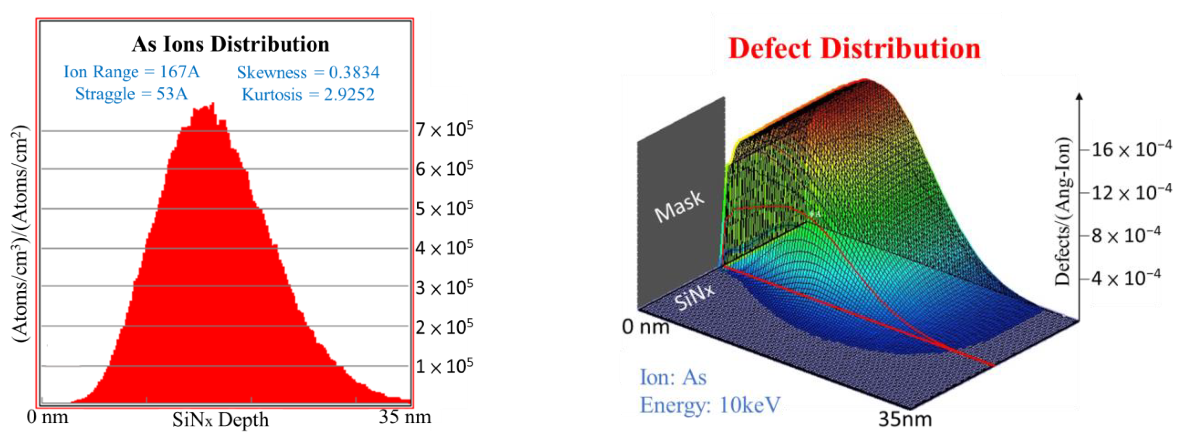
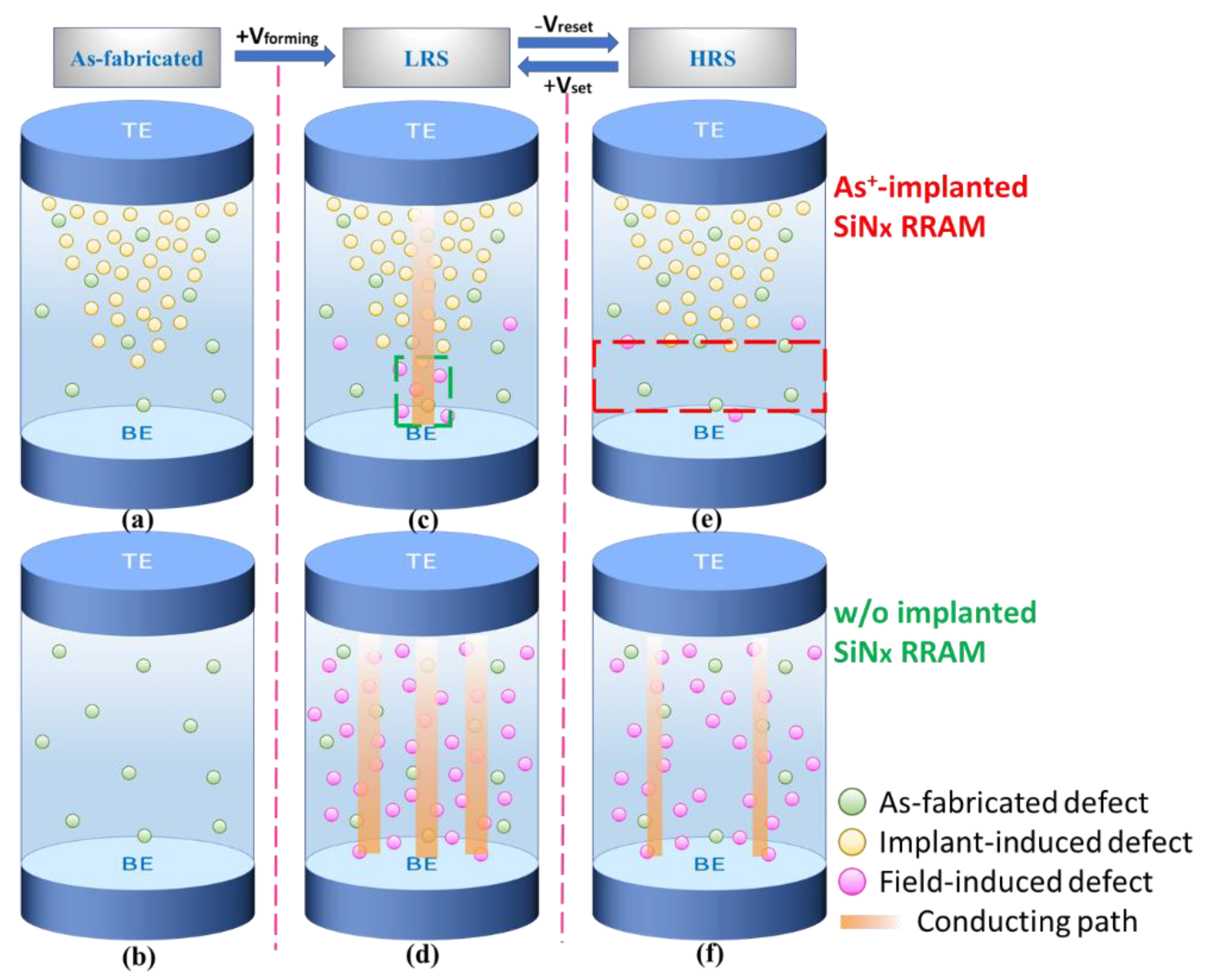
3. Results
4. Conclusions
Supplementary Materials
Author Contributions
Funding
Institutional Review Board Statement
Informed Consent Statement
Data Availability Statement
Acknowledgments
Conflicts of Interest
References
- Waser, R.; Aono, M. Nanoionics-based resistive switching memories. Nat. Mater. 2007, 6, 833–840. [Google Scholar] [CrossRef]
- Pan, F.; Gao, S.; Chen, C.; Song, C.; Zeng, F. Recent progress in resistive random access memories: Materials, switching mechanisms and performance. Mater. Sci. Eng. R 2014, 83, 1–59. [Google Scholar] [CrossRef]
- Wong, H.S.P.; Lee, H.Y.; Yu, S.; Chen, Y.S.; Wu, Y.; Chen, P.S.; Lee, B.; Chen, F.T.; Tsai, M.J. Metal–Oxide RRAM. Proc. IEEE 2012, 100, 1951–1970. [Google Scholar] [CrossRef]
- Zahoor, F.; Azni Zulkifli, T.Z.; Khanday, F.A. Resistive random access memory (RRAM): An overview of materials, switching mechanism, performance, multilevel cell (mlc) storage, modeling, and applications. Nanoscale Res. Lett. 2020, 15, 90. [Google Scholar] [CrossRef]
- Shen, Z.; Zhao, C.; Qi, Y.; Xu, W.; Liu, Y.; Mitrovic, I.Z.; Yang, L.; Zhao, C. Advances of RRAM Devices: Resistive Switching Mechanisms, Materials and Bionic Synaptic Application. Nanomaterials 2020, 10, 1437. [Google Scholar] [CrossRef]
- Gao, B.; Wu, H.; Wu, W.; Wang, X.; Yao, P.; Xi, Y.; Zhang, W.; Deng, N.; Huang, P.; Liu, X.; et al. Modeling disorder effect of the oxygen vacancy distribution in filamentary analog RRAM for neuromorphic computing. In Proceedings of the 2017 IEEE International Electron Devices Meeting (IEDM), San Francisco, CA, USA, 2–6 December 2017; pp. 91–94. [Google Scholar]
- Wong, H.-S.P.; Salahuddin, S. Memory leads the way to better computing. Nat. Nanotechnol. 2015, 10, 191–194. [Google Scholar] [CrossRef] [PubMed]
- Hickmott, T.W. Low-frequency negative resistance in thin anodic oxide films. J. Appl. Phys. 1962, 33, 2669. [Google Scholar] [CrossRef]
- Yu, S.; Guan, X.; Wong, H.S.P. Conduction mechanism of TiN/HfO(x)/Pt resistive switching memory: A trap-assisted-tunneling model. Appl. Phys. Lett. 2011, 99, 063507. [Google Scholar] [CrossRef]
- Cheng, C.H.; Chin, A.; Yeh, F.S. Novel ultra-low power RRAM with good endurance and retention. In Proceedings of the 2010 Symposium on VLSI Technology, Honolulu, HI, USA, 15–17 June 2010; pp. 85–86. [Google Scholar]
- Cheng, C.H.; Chou, K.Y.; Chin, A.; Yeh, F.S. Very high performance non-volatile memory on flexible plastic substrate. In Proceedings of the 2010 International Electron Devices Meeting, San Francisco, CA, USA, 6–8 December 2010; pp. 512–515. [Google Scholar]
- Cheng, C.H.; Chen, P.C.; Wu, Y.H.; Yeh, F.S.; Chin, A. Long endurance nano-crystal TiO2 resistive memory using TaON buffer layer. IEEE Electron Device Lett. 2011, 32, 1749–1751. [Google Scholar] [CrossRef]
- Yen, T.J.; Gismatulin, A.; Volodin, V.; Gritsenko, V.; Chin, A. All nonmetal resistive random access memory. Sci. Rep. 2019, 9, 6144. [Google Scholar] [CrossRef]
- Gismatulin, A.A.; Gritsenko, V.A.; Yen, T.J.; Chin, A. Charge transport mechanism in SiNx-based memristor. Appl. Phys. Lett. 2019, 15, 253502. [Google Scholar] [CrossRef]
- Yen, T.J.; Chin, A.; Gritsenko, V. High performance all nonmetal SiNx resistive random access memory with strong process dependence. Sci. Rep. 2020, 10, 2807. [Google Scholar] [CrossRef] [PubMed]
- Kim, S.; Cho, S.; Ryoo, K.C.; Park, B.G. Effects of conducting defects on resistive switching characteristics of SiNx-based resistive random-access memory with MIS structure. J. Vac. Sci. Technol. 2015, 33, 0662201. [Google Scholar] [CrossRef]
- Chen, Y.D.; Chin, A. An offset readout current sensing scheme for one-resistor RRAM-based cross-point array. IEEE Electron Device Lett. 2019, 40, 208–211. [Google Scholar] [CrossRef]
- Zackriya, M.; Kittur, H.M.; Chin, A. A novel read scheme for large size one-resistor resistive random access memory array. Sci. Rep. 2017, 7, 42375. [Google Scholar] [CrossRef]
- Gao, B.; Kang, J.F.; Chen, Y.S.; Zhang, F.F.; Chen, B.; Huang, P.; Liu, L.F.; Liu, X.Y.; Wang, Y.Y.; Tran, X.A.; et al. Oxide-based RRAM: Unified microscopic principle for unipolar and bipolar switching. In Proceedings of the 2011 International Electron Devices Meeting, Washington, DC, USA, 5–7 December 2011; pp. 420–423. [Google Scholar]
- Lee, S.; Kim, H.; Yun, D.J.; Rhee, S.W.; Yong, K. Resistive switching characteristics of ZnO thin film grown on stainless steel for flexible nonvolatile memory devices. Appl. Phys. Lett. 2009, 95, 262113. [Google Scholar] [CrossRef]
- Lim, E.W.; Ismail, R. Conduction mechanism of valence change resistive switching memory: A survey. Electronics 2015, 4, 586–613. [Google Scholar] [CrossRef]
- Fang, R.; Chen, W.; Gao, L.; Yu, W.; Yu, S. Low temperature characteristics of HfOx-based resistive random access memory. IEEE Electron Device Lett. 2015, 36, 567–569. [Google Scholar] [CrossRef]
- Zhang, Y.; Deng, N.; Wu, H.; Yu, Z.; Zhang, J.; Qian, H. Metallic to hopping conduction transition in Ta2O5−x/TaOy resistive switching device. Appl. Phys. Lett. 2014, 105, 063508. [Google Scholar] [CrossRef]
- Yu, L.E.; Kim, S.; Ryu, M.K.; Choi, S.Y.; Choi, Y.K. Structure effects on resistive switching of Al/TiOx /Al devices for RRAM applications. IEEE Electron Device Lett. 2008, 29, 331–333. [Google Scholar]
- Kim, S.; Jeong, H.Y.; Choi, S.Y.; Choi, Y.K. Comprehensive modeling of resistive switching in the Al/TiOx/TiO2/Al heterostructure based on space-charge-limited conduction. Appl. Phys. Lett. 2010, 97, 2–4. [Google Scholar] [CrossRef]
- Wang, S.Y.; Huang, C.W.; Lee, D.Y.; Tseng, T.Y.; Chang, T.C. Multilevel resistive switching in Ti/CuxO/Pt memory devices. J. Appl. Phys. 2010, 108, 114110. [Google Scholar] [CrossRef]
- Available online: https://en.wikipedia.org/wiki/Arsenic (accessed on 16 March 2021).
- Yen, T.J.; Chin, A.; Gritsenko, V. Exceedingly high performance top-gate p-type SnO thin film transistor with a nanometer scale channel layer. Nanomaterials 2021, 11, 92. [Google Scholar] [CrossRef]
- Chiu, F. A review on conduction mechanisms in dielectric films. Adv. Mater. Sci. Eng. 2014, 2014, 578168. [Google Scholar] [CrossRef]


| Reference | Switching Layer Materials | Thickness (nm) | CVs of Vset and Vreset (D2D) | CVs of Vset and Vreset (C2C) |
|---|---|---|---|---|
| 15 | PECVD-SiNx | 25 | 18.3%/23.2% | 14%/21.4% |
| 15 | PVD-SiNx | 25 | 10.7%/12.1% | 11.3%/11.4% |
| 16 | PECVD-SiNx | 7.5 | 29%/17.77% | -- |
| 16 | LPCVD-SiNx | 7.5 | 16%/7.59% | -- |
| This work | As+-implanted PECVD-SiNx | 35 | 10.7%/9.8% | 2.2%/3.8% |
Publisher’s Note: MDPI stays neutral with regard to jurisdictional claims in published maps and institutional affiliations. |
© 2021 by the authors. Licensee MDPI, Basel, Switzerland. This article is an open access article distributed under the terms and conditions of the Creative Commons Attribution (CC BY) license (https://creativecommons.org/licenses/by/4.0/).
Share and Cite
Yen, T.-J.; Chin, A.; Gritsenko, V. Improved Device Distribution in High-Performance SiNx Resistive Random Access Memory via Arsenic Ion Implantation. Nanomaterials 2021, 11, 1401. https://doi.org/10.3390/nano11061401
Yen T-J, Chin A, Gritsenko V. Improved Device Distribution in High-Performance SiNx Resistive Random Access Memory via Arsenic Ion Implantation. Nanomaterials. 2021; 11(6):1401. https://doi.org/10.3390/nano11061401
Chicago/Turabian StyleYen, Te-Jui, Albert Chin, and Vladimir Gritsenko. 2021. "Improved Device Distribution in High-Performance SiNx Resistive Random Access Memory via Arsenic Ion Implantation" Nanomaterials 11, no. 6: 1401. https://doi.org/10.3390/nano11061401
APA StyleYen, T.-J., Chin, A., & Gritsenko, V. (2021). Improved Device Distribution in High-Performance SiNx Resistive Random Access Memory via Arsenic Ion Implantation. Nanomaterials, 11(6), 1401. https://doi.org/10.3390/nano11061401