Review

Low-Toxic, Earth-Abundant Nanostructured Materials for Thermoelectric Applications

1
Department of Electrical Engineering, College of Engineering, Qatar University, Doha 2713, Qatar
2
Qatar University Young Scientist Center (YSC), Qatar University, Doha 2713, Qatar
3
Center for Advanced Materials (CAM), Qatar University, Doha 2713, Qatar
*
Author to whom correspondence should be addressed.
Nanomaterials 2021, 11(4), 895; https://doi.org/10.3390/nano11040895
Submission received: 5 March 2021 / Revised: 27 March 2021 / Accepted: 30 March 2021 / Published: 31 March 2021

Abstract

:
This article presents recent research directions in the study of Earth-abundant, cost-effective, and low-toxic advanced nanostructured materials for thermoelectric generator (TEG) applications. This study’s critical aspect is to systematically evaluate the development of high-performance nanostructured thermoelectric (TE) materials from sustainable sources, which are expected to have a meaningful and enduring impact in developing a cost-effective TE system. We review both the performance and limitation aspects of these materials at multiple temperatures from experimental and theoretical viewpoints. Recent developments in these materials towards enhancing the dimensionless figure of merit, Seebeck coefficient, reduction of the thermal conductivity, and improvement of electrical conductivity have also been discussed in detail. Finally, the future direction and the prospects of these nanostructured materials have been proposed.

1. Introduction

An ideal thermoelectric (TE) material should have the thermal properties of the glass and electrical properties of a crystal, also known as “phonon glass electron crystal” [1]. A common strategy for improving the performance of the conventional TE materials is to reduce thermal conductivity by introducing nanometer-scale grains or interfaces that scatter the heat-carrying phonons [2,3,4]. But improving the electrical conductivity and decreasing the thermal conductivity of materials is always a challenge due to their interdependent nature. In the nanostructured materials, the lower lattice thermal conductivity is observed because of the efficient scattering of phonons over an extensive mean free path range by a high density of interfaces. The efficiency of a TE material can be defined in terms of the figure of merit(Z) of the materials [5] is given by:
Z = α p α n 2 ( ( k p · ρ p ) 1 / 2 + ( k n · ρ n ) 1 / 2 ) 2
where α p & α n are the Seebeck coefficients of the two materials of the thermocouple, ρ p & ρ n are the electrical resistivities, and k p & k n are the thermal conductivities.
ZT is the product of the average temperature and the figure of merit and is called the dimensionless figure of merit and for a single material can be given by:
Z T = α 2 T k ρ = α 2 σ T k
T = T H T C / 2
where, T H is the hot side temperature, T C is the cold side temperature of the modules, σ and k are the electrical and thermal conductivity of the material, respectively.
The maximum ZT has been achieved by reducing the thermal conductivity through nanostructured engineering or hierarchal architecting [6]. Nevertheless, the high cost and toxicity are barriers to the real-life application of these nanostructured materials in TEGs [7]. The preliminary materials that were being used for TE applications were tellurides doped with bismuth, antimony, and lead, etc. However, due to their high cost and toxicity, these TE materials were only used for cooling and power generation applications, where the price was not the primary concern. Later, with the discovery of silicon-germanium (SiGe), the TEGs were principally employed to convert heat into power in spacecraft designed for deep-space NASA missions. Due to these materials’ expensiveness and toxicity, it has not been possible to utilize them in widespread and daily-life applications. Hence, it was highly desirable to develop low-cost and low-toxic TEGs with high ZT value, using materials that are abundant, low toxic, and easy to synthesize. Thus, TE materials such as clathrates, skutterudites, half-Heuslers, oxide, silicides, chalcogenides, and selenides have been proposed. Elemental doping, nanostructuring, nanowiring, nano-inclusion, and ball milling techniques have been used to enhance the ZT value in these materials.
This review spotlights materials made from sustainable, Earth-abundant, cost-effective, and low-toxic elements that have the potential to replace conventional lead telluride, i.e., skutterudites made from rare-earth elements. These TE materials can provide a prospective low-cost solution to deal with the energy crisis by utilizing waste heat and concentrated solar power. In these TE materials, the rattlers, vacancies, and voids can significantly reduce thermal conductivity and improve the ZT value. The “phonon glass electron crystal” characteristics of these cost-effective and non-toxic materials can remarkably be enhanced by producing their nanowires and nanocomposites. Here it is important to mention that in this review the choice of the materials was done based on the factor which include cost, performance, and relatively low toxicity. Of course, the toxicity of the material is sometimes difficult to completely avoid if we consider all three factors.

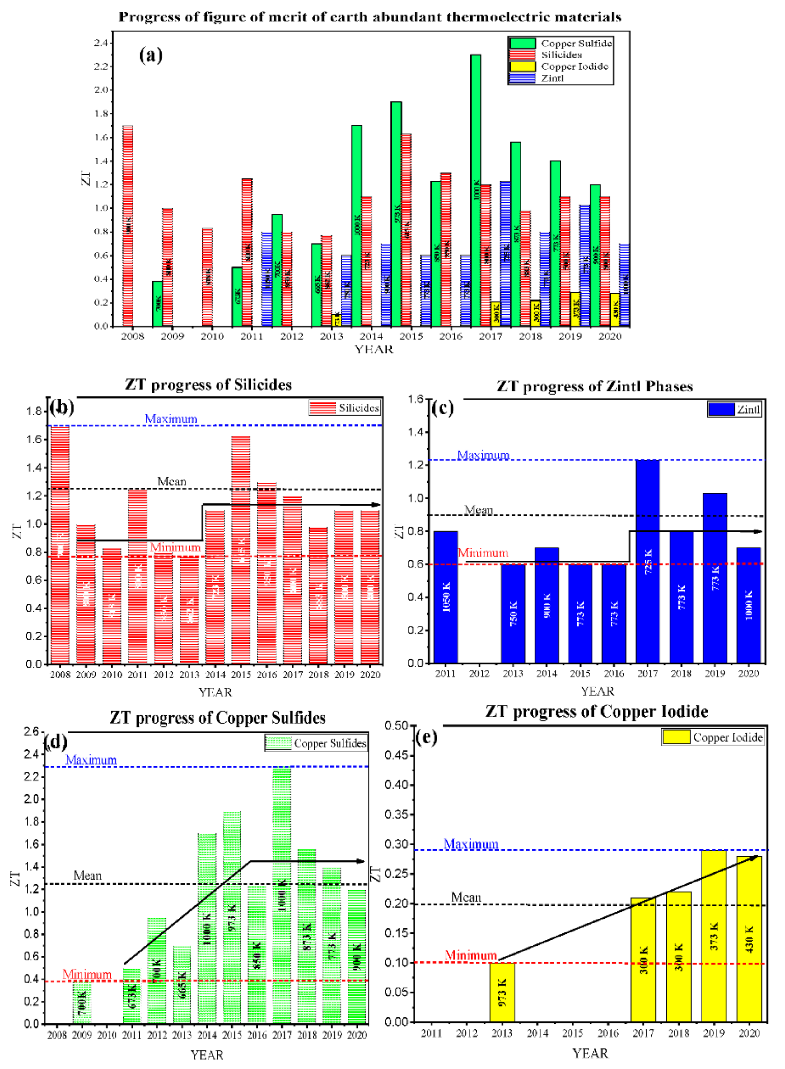
2. Recent Advancements

Figure 1a represents recent advancements in the low-toxic and earth-abundant TE materials, and their figure of merit (ZTmax) attained at low, intermediate, and high temperatures. These materials are sufficiently available and harmlessly disposable and consist of various low toxic silicides, Zintl compounds, and copper-base alloys, including copper sulfides and copper iodides. These materials possess enormous advantages and have room for further improvements, making them potential competitors to the traditional TE materials. For instance, silicides such as silicon germanium are available since the first synthesis of thermoelectric materials. They are mainly used in space applications, with the only drawback of germanium’s high fabrication cost, but over time, the researchers have resolved this issue by using lower amounts of germanium or replacing germanium with low-toxic and abundantly available materials such as magnesium, manganese, chromium, etc. Along with silicon, these materials form various silicides that have both the benefits of traditional silicides and eco-friendliness. The ZT value for such silicides has been successfully attained >1; even, in some cases, it has been reported to be over 1.5 (see Figure 1b).
Similarly, the Zintl compounds are a subgroup of intermetallic compounds, initially comprising toxic and rare-earth materials, but lately, a few Zintl compounds, such as Ca3AlSb3, Mg3Sb2, CaAl2Si2, etc., have also been developed that have the benefits of Zintls as well as low toxicity and abundancy. Low-toxic Zintls likewise have good potential for commercialization for heat recovery applications. The average ZT value for such materials lies in the range of 0.8 ± 0.2, as shown in Figure 1c. Figure 1d shows that copper sulfides (with a mean ZT value >1.2) also exhibit great potential for the intermediate and high-temperature range of low-toxic and geo abundant thermoelectric materials. In a case study of copper sulfides doped with trace amounts of rare-earth chalcogenides, the highest ZT value >2 is reported. However, low values of ZT have been observed in copper iodide and its alloys, as shown in Figure 1e. In the low-temperature range applications, copper iodide is a transparent and flexible thermoelectric material. Its maximum ZT value is deficient (~0.3) compared to other TE materials in this temperature range.

3. Temperature-Dependent Classification of Low-Toxic Earth-Abundant Thermoelectric Materials

The TE materials are classified into three categories based on their operating temperatures: low temperature, medium or intermediate temperature, and high temperature. In this section, we discuss the temperature-dependent types of low-toxic and earth-abundant thermoelectric materials.

3.1. Low-Temperature Thermoelectric Materials

In a low-temperature range, copper iodide (CuI) is a promising candidate as a low-toxic and Earth-abundant material. CuI can be a potential alternative to the commercially available low-temperature TE materials such as bismuth telluride. It is abundantly available and can find its applications in smart screens or windows, portable and wearable energy devices due to its flexible and transparent nature [6,8,9]. It can be seen from Figure 2a the optical transmittance spectra of the CuI exhibits ~60–85% transmittance in the wavelength range 410–2000 nm. High power density with good mechanical flexibility has been noticed in the prototype CuI-based module [10]. The Seebeck coefficient and power factor were attained up to ~431 µVK−1 and ~70 µWm−1K−2, respectively, by tuning the defect iodine chemistry via thermal annealing; the best thermoelectric properties were observed at moderate annealing temperatures (~430 K) [10] as illustrated in Figure 2b.
Typically, the transparent TE materials show low electrical conductivities resulting in inferior TE properties. However, a transparent TEG consisting of p-type CuI and n-type gallium doped zinc oxide (GZO) with high electrical conductivity 110 Scm−1 and ZTmax of 0.22 at 300 K, has been fabricated by Faustino et al. [11]. The GZO thin film was prepared using different fabrication including, solid iodization, thermal evaporation, and vapor deposition method. The SEM images of nanostructured CuI synthesized using the above-mentioned methods are depicted in Figure 2c. A clear difference in the size of the nanostructures is observed, and this study reveals that the CuI film prepared by solid iodination of Cu works better in both TE characteristics and in terms of optical transparency. Later on, Coroa et al. [12] constructed a transparent flexible thermoelectric generator using 17 p-n modules on a polyimide Kapton® CS substrate, where CuI and GZO were used as p-type and n-type materials, respectively as shown in Figure 2d and sketched in Figure 2e.
Further, 300 nm thick CuI film doped with terbium (Tb) single nanocrystal demonstrated a ZTmax value of 0.29. The illustration of the Tb-doped CuI structure is given in Figure 2f, which can be operated at 430 K [13]. The current ZT progress of CuI-based TE materials is given in Table 1. The maximum ZT of these materials is ~0.3, which is way less than other materials in this temperature range.

3.2. Intermediate Temperature Thermoelectric Materials

In the medium temperature range, TE materials (ranging between 500–900 K) include chalcogenides skutterudites, tin, half-heusler, etc. Chalcogenides such as sulfur alloys are appropriate low-toxic and low-cost materials in this temperature range and can be used for waste heat recovery. The sulfide-based chalcogenides investigated for the TE applications include copper sulfide (CuxSy), copper zinc tin sulfide (CZTS), bismuth sulfide iodide (BiSI), silicon sulfide (SiS), and silicon selenide (SiSe).

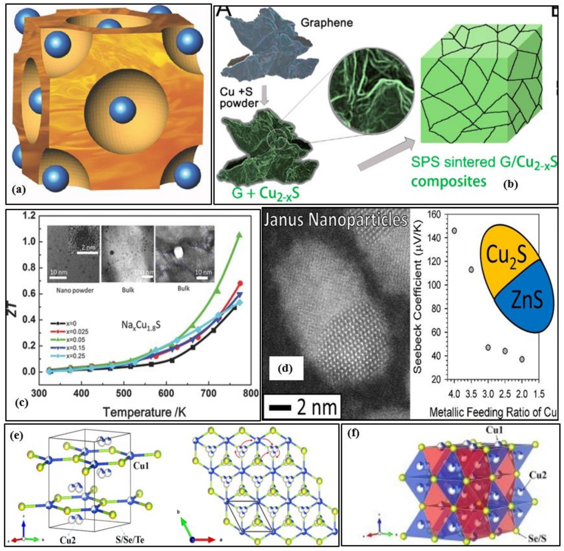
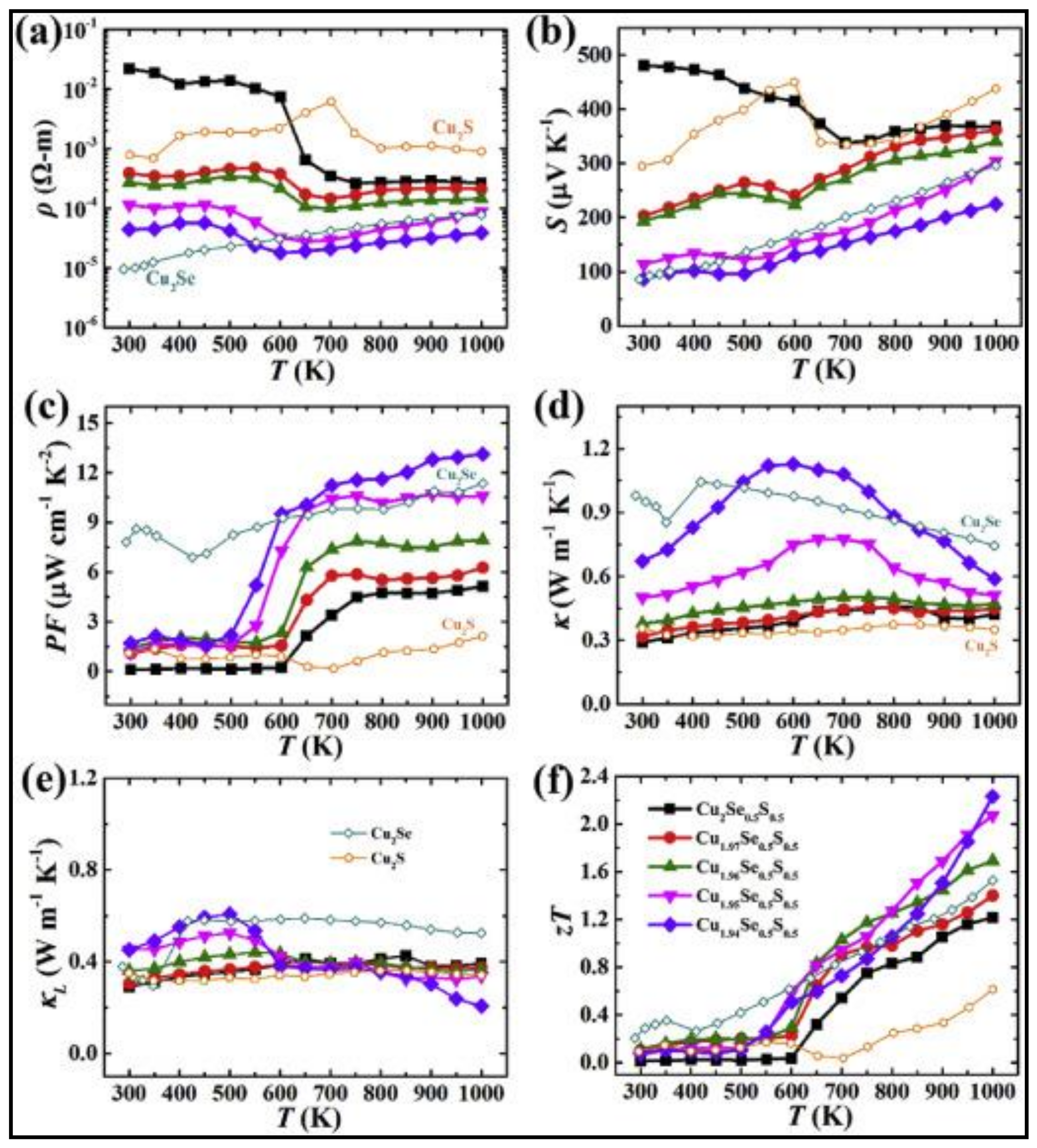
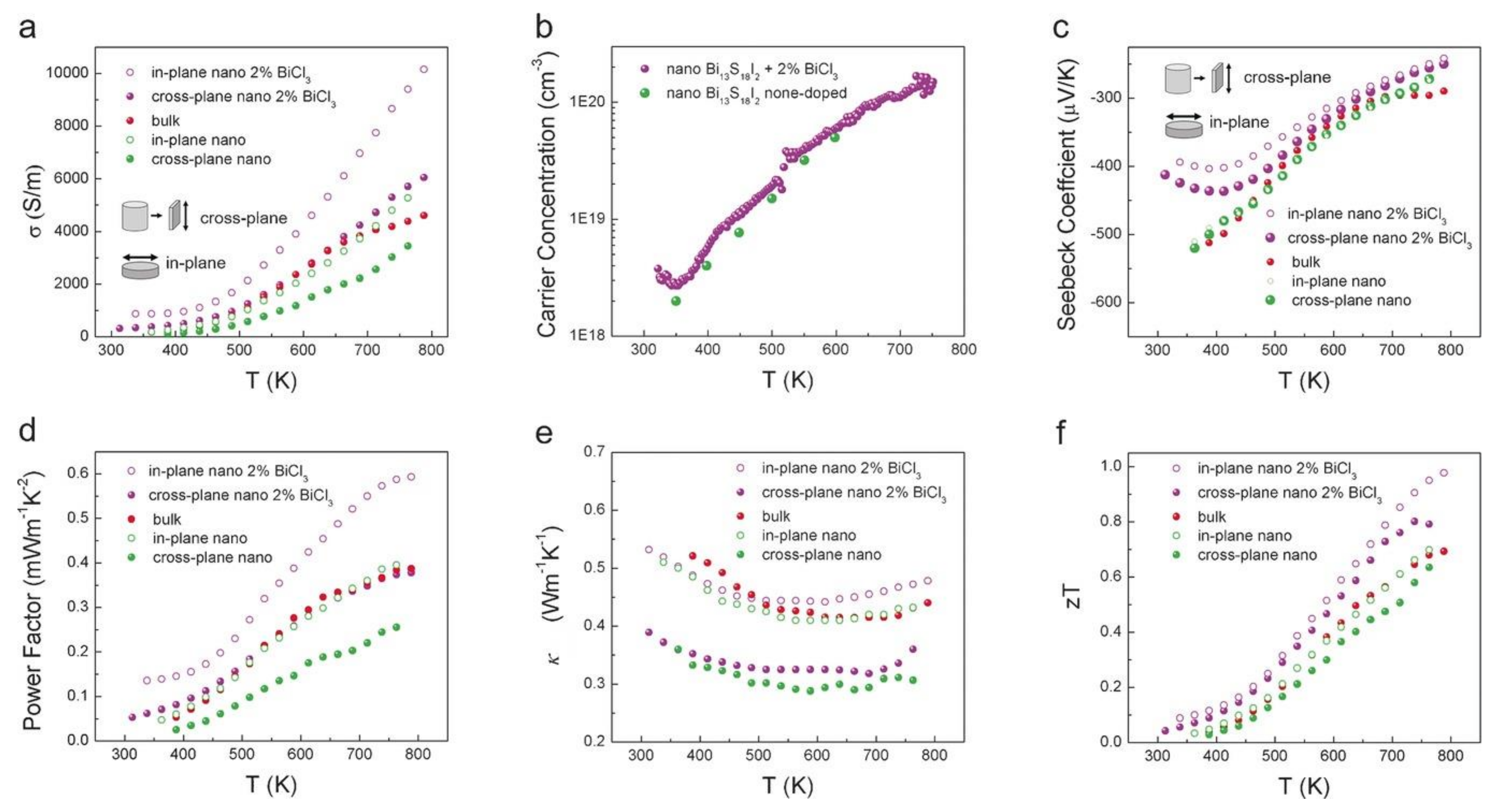
3.2.1. Chalcogenides (Sulfur-Based)

The properties and structures of copper sulfide-based thermoelectric materials such as chalcopyrite (CuFeS2), chalcocite (Cu2S), bornite (Cu5FeS4), kesterite (Cu2SnS4), stannite (Cu2FeSnS4), tetrahedrite [(Cu, Fe)12Sb4S13], and colusite [Cu26V2(As,Sn, Sb)6S32] have been reviewed [14]. Wei et al. presented a complete review of the family of copper chalcogenides (Cu2X, where X = S, Te, Se) from their structural features to design strategies to device development [15]. The primary concern is the volatilization of sulfur during synthesis and under higher temperature operations, thereby affecting the material stability. The loss of sulfur leads to changes in the nominal stoichiometries making reproducibility challenging to achieve. Also, the mobile copper ions migrate and form a layer at one end of the thermoelement under the electric field created when the device is operated at a temperature gradient resulting in lower performance, cracking, and compositional changes. A theoretical evaluation of the potential properties and stability of Fe-doped Cu2S was performed [16]. Some other works also showed this problem of Cu ions migration under working conditions [17,18,19,20]. One possible method to avoid this is by doping of bulk Cu2S with low mobility ions that can concurrently behave as electron-donors e.g., Fe [21]. Figure 3a shows the crystal structure of the chalcocite α phase of copper sulfide (Cu2−xS). The free copper ions travel and migrate freely in the sulfide sublattice (the blue spheres represent the sulfur atoms). Even though, in some case of CuxSy based TE materials, the ZT value has been exceeded over unity as shown in Figure 3c, however, mostly ZT > 0.6 is realized in p-type copper sulfides, but for n-type, the ZT value is even inferior. Tang et al. [22] suggested the introduction of a 3D graphene heterointerface via a combination of mechanical alloying and spark plasma sintering into the Cu2−xS matrix to improve the Seebeck coefficient and limit the thermal conductivity. A very high power factor and peak ZT of 1197 µWm−1K−2 and 1.56 at 873 K is attained for 0.75 wt%G/Cu2−xS with excellent tested reproducibility after five cycles [22]. Figure 3b shows the schematic illustration of the synthesis of G/Cu2−xS composite via spark plasma sintering. The addition of grain boundaries and interfaces in the Cu2S material through the dispersion of carbon nanotube(CNT) has restricted the thermal conductivity to less than 0.4 Wm−1K−1 at 448–798 K [23]. The Seebeck Coefficient reached up to 388 µVK−1 at 800 K due to the energy barrier filtering, and a peak ZT of 0.74 at 750 K was attained in the composite with a 10% CNT molar ratio [23]. Table 2 presents some prominent works in nanostructured copper sulfide materials for the past five years. Several novel methods were experimented to develop highly efficient nanostructured copper sulfides. Tang et al. [24] fabricated hexagonal sheet-like copper sulfide (Cu2S) nanocrystals of thickness 5–20 nm by the wet chemistry method and later densified by spark plasma sintering to obtain a high figure of merit of 0.62 at 773. This method can be used to synthesize large-scale copper sulfide bulk materials, and the results indicated that the phase structures and morphologies were highly influenced by the reaction time and temperature. Mulla et al. [25] suggested a novel rapid, and simple ambient chemical route to grow highly oriented and dense dendrites of Cu2S on a copper substrate and doping with copper ions to form uniform films covered with dense nanosheets. This cost-effective synthesis technique increased the Seebeck coefficient from ~100 to 415 µVK−1 and a high-power factor of ~400 µWm−1K−2.
Various materials such as sodium, tungsten, etc., are less toxic and widely available and are used as dopants to the nanostructured copper sulfides to enrich their thermoelectric properties. Single doping or dual doping leads to the introduction of nanoprecipitation or point defects or faults/stacking in the host structures, thereby influencing the thermoelectric performance. Cu1.8S + 3 wt% In2S3 bulk samples were fabricated by doping with indium sulfide(In2S3) by spark plasma sintering to reach a peak ZT of 1.4 at 773 K [26]. The fast doping resulted in point defects, nanopores, and inclusion of second phases in the Cu1.8S bulk materials [26]. These nanostructures dropped the thermal conductivity, and the indium doping enhanced the effective mass of the charge carriers improving the Seebeck coefficient [26]. Nanoscale CuInS2 phase was formed with the introduction of 2% indium sulfide (In2S3) to reach a ZT value of 1.23 and a relatively high-power factor of 1361 µWm−1K−2 at 850 K [27]. The introduction of Bi2S3 and Bi2S3@Bi core-shell nanostructured rods to the low-toxic geo abundant digenite (Cu1.8S) has increased the maximum figure of merit to 0.77 at 723 K (in the case of 3% wt Bi2S3@Bi core-shell nanorods), which is significantly higher than the pristine Cu1.8S [28]. Through the dispersion of 1.0 wt% SiC into the polycrystalline p-type Cu1.8S, a peak figure of merit of 0.87 at 773 K was attained by optimizing the carrier concentration, thereby reducing the thermal conductivity [29]. Doping the p-type Cu1.8S with tungsten diselenide (WSe2) has significantly enhanced the thermoelectric properties when compared to pristine p-type Cu1.8S (0.49 at 773) [30]. The WSe2 nanoparticles and their refined grain size have significantly decreased the thermal conductivity, and the optimized carrier concentration simultaneously enhanced the Seebeck Coefficient [30]. The peak ZT, Seebeck coefficient, and thermal conductivity of Cu1.8S + 1 wt% WSe2 sample at 773 K is 1.22, 110 µVK−1, and 0.68 Wm−1K−1, respectively [30]. The NaxCu9S5(x = 0.025,0.05,0.15,0.25) nanopowders were sintered to fabricate p-type NaxCu9S5 bulk materials via spark plasma sintering with an average size of 3 nm, and remarkable high ZT of ~1.1 and low thermal conductivity of 0.7 Wm−1K−1 at 773 K was observed by optimized carrier concentration and introduction of nanopores due to Na-doping (x = 0.05) [31]. Figure 3c shows the temperature dependence of the figure of merit ZT value for Cu9S5 samples with different sodium contents. The TEM image shown in the inset shows the nanostructure of Na1−xCu9S5 powders.
Cu2−yS has exceptionally low thermal conductivity, while Cu2−ySe has efficient electrical transport properties. Combining these extraordinary characters into one solid material will result in exceptional thermoelectric performance. A nanoscale mosaic hexagonal structured component Cu2−yS1/3Se1/3Te1/3 solid solutions consisting of 10–30 nm-sized mosaic grains using three matrix compounds Cu2S, Cu2Se, and Cu2Te is synthesized to reach a superior ZT of 1.9 at 1000 K and y = 0.02 [32]. The schematic illustration of the hexagonal crystal structure of Cu2−yS1/3Se1/3Te1/3 is shown in Figure 3e. Each unit cell is shared with one S/Se/Te site and two copper sites. The projected plane representation of the crystal structure through the [001] direction can also be seen. The copper ions can travel among different copper sites, as indicated by the red arrow. The partial coloring of the atoms shows the atomic site occupancy. The reason for this exceptionally high ZT is its low thermal conductivity of ~0.49 Wm−1K−1 due to the phonon scattering by point defects, lattice strains of mosaic nanograins, and liquid-like copper ions. Zhao et al. [33] focused on this concept and formed a solid solution of Cu2−ySe0.5S0.5 with half sulfur and half selenium, and the resulting material possessed a unique hierarchical microstructure comprising of nanoscale domains, mesoscale polymorphs, and modulations. Figure 3f shows the visualization of the crystal structure of Cu2−ySe0.5S0.5 fabricated at 100 K. The disordered Cu2 sites are illustrated by blue tetrahedron and Cu1 sites by red octahedron. The tuning of its native Copper vacancies significantly improved its electrical transport properties and remarkably extraordinary thermoelectric performance with the maximum figure of merit of 2.3 at 1000 K and very low thermal conductivity of ~0.32 Wm−1K−1 at 1000 K is noted. This is up to date the highest value the figure of merit has reached in the case of chalcogenide bulk materials. Figure 4a–f summarize the thermoelectric properties of Cu2−ySe0.5S0.5, namely the electrical conductivity, Seebeck coefficient, power factor, total thermal conductivity, lattice thermal conductivity, and figure of merit ZT. It is to be noted that Cu2Se0.5S0.5 had better electrical conductivity and Seebeck coefficient but lags in terms of power factor, and Z.T. Cu1.94Se0.5S0.5 had the best ZT value due to lower lattice conductivities at 1000 K. In another solid solution material, Cu2S0.5Te0.5, multiform nanostructures such as nano-domains of ordered structure, 4H polytype, mosaic nanocrystals, high density of stacking faults, and nanoscale periodic antiphase boundaries have been observed, resulting in ultra-low lattice thermal conductivity <0.4 and peak ZT of about 1.9 [34]. The multiformity of the material coincides with the phonon-glass-electron-crystal concept for extremely high-performance thermoelectric material.
Figure 3d shows the schematic illustration of the STEM-HAADF image of copper sulfide-zinc sulfide Janus nanoparticles (2 nm in size) and the dependence of the Seebeck coefficient on the metallic feeding ratio of copper. The Seebeck coefficient is high in the case of pristine CuS, and as the ZnS nanoparticle contents increase, the Seebeck coefficient decreases due to dilution of the material [35]. Copper zinc tin sulfide (CZTS) elements are low-toxic and extremely abundant. The electrical conductivity and figure of merit of CZTS have significantly improved, and thermal conductivity is lowered by doping the CZTS nanocrystal material with copper; however, there has been a decline in the Seebeck coefficient, and this may be due to the higher carrier concentration from copper doping. The copper tin sulfide (CTS) has the benefit of disordered metal atoms arrangement in the cubic and tetragonal phases, and it also has a distinct electronic nature that is influenced by the S-3p and Cu-3d orbitals, which gives place to independent variation of carrier concentration through heavy doping with no effect on the valence band. Based on these beneficial properties, a p-type CuSnS3 doped with zinc (20%) was synthesized using spark plasma sintering to form a 3-dimensionally conductive network for holes resulting in ultra-low thermal conductivity of ~0.9 ± 0.4 Wm−1K−1, and a high power factor of ~0.84 mWm−1K−2 at 723 K [36]. The addition of tin in the pristine Cu1.8S introduces a second phase to optimize the carrier concentration and formation of nanopores to reduce the thermal conductivity k. An ultra-low thermal conductivity and a high ZT value of 0.30 W/mK and 0.81 respectively at 773 K is recorded in the case of Sn0.01Cu1.79S bulk material [37]. Two heterogeneous phases (Cu12Sb4S13 and Cu4SnS4) were induced due to Sb/Sn co-doping that rapidly declined the carrier concentration and enriched the phonon scattering to record a high ZT of 1.2 at 773 K for Cu1.8Sb0.02Sn0.03S bulk sample [38].
Figure 3. (a) The crystal structure of the cubic-chalcocite α phase of Cu2−xS (the sulfur atoms are represented by the blue spheres), Reproduced with permission from [39]. Copyright © 2014, Wiley Online Library, (b) Schematic representation of the spark plasma sintering process for fabricating graphene/Cu2−xS nanocomposites, Reproduced with permission from [22]. Copyright © 2018, Elsevier, (c) The temperature dependence of figure of merit ZT value for Cu9S5 sample with different sodium contents. The inset shows nanostructure in the TEM image of Na1−xCu9S5 powders, Reproduced with permission from [31]. Copyright © 2016, Wiley Online Library, (d) Schematic Illustration of STEM-HAADF image of copper sulfide-zinc sulfide Janus nanoparticles at 2nm size and dependence of the Seebeck coefficient on the metallic feeding ratio of copper, Reproduced with permission from [35]. Copyright © 2016, ACS Publications. (e) Visualization of the crystal structure with a space group (P63/mmc) at 100 K of Cu2−yS1/3Se1/3Te1/3 (Hexagonal structure), Reproduced with permission from [32]. Copyright © 2017, Elsevier., (f) Visualization of the crystal structure with a space group (P63/mmc) at 100 K of Cu2Se0.5S0.5, Reproduced with permission from [33]. Copyright © 2017, Elsevier.
Nanomaterials 11 00895 g003
Table 2. Prominent copper-sulfide nanostructured alloys/composites reported from 2016–2020.
Sr.noMaterialOperating
Temperature (K)
Synthesis Techniqueσ *
(Scm−1)
k *
(Wm−1K−1)
Seebeck
Coefficient (µVK−1)
PF *
(S2σ/µWm−1K−2)
ZT *maxYear/Reference
120%Zn-Doped Cu2SnS3723Spark plasma Sintering~6000.9 ± 0.4~1008400.582016 [36]
2Na0.05Cu9S5773Mechanical Alloying
Spark Plasma Sintering
~8500.7~11010501.12016 [31]
3Cu2S with 2%wt In2S3850Spark Plasma Sintering~5000.9520013611.232016 [27]
4SnxCu1.8-xS at x = 0.01773Planetary ball mining
Spark Plasma Sintering
190.4250~5000.812017 [37]
5Cu1.98S1/3Se1/3Te1/31000Spark Plasma SinteringN/A~0.4925011201.92017 [32]
6Cu2S NS doped with Cu ion300–360Simple room temperature chemical routeN/AN/A415~400N/A2017 [25]
7Cu2−ySe0.5S0.51000Spark Plasma SinteringN/A0.3237015002.32017 [33]
8αCu2S (1–7 µm)
βCu2S (5–20 nm)
573
773
Hydrothermal synthesis
Wet chemistry method
~100
~1000
~0.2
~1.23
~420
101
196
985
0.38
0.62
2017 [24]
9Cu2.14Co0.8Mn0.05SnS4 (Cu/Mn co-doping)800Mechanical Alloying
Hot Pressed Sintering
N/A~1.0~20010260.82017 [40]
10Cu2S0.5Te0.5-Spark Plasma SinteringN/A<0.4N/AN/A1.92017 [34]
11Cu1.8S with 3% wt Bi2S3@Bi core-shell nanorods723Mechanical Alloying
Spark Plasma Sintering
~15000.9185~9900.772017 [28]
12Polycrystalline p-type Cu1.8S with 1.0 wt% SiC NP *773Mechanical Alloying
Spark Plasma Sintering
~9000.7115~9000.872017 [29]
13Cu1.0Fe0.97S2.12(S1.96)(Fe−1-S) n-type623Hot injection
Sintering
8500.5238N/A0.132017 [41]
14Cu5FeS4 Bornite NP320Mechanical Alloying AnnealingN/A0.461302500.282018 [42]
15Cu2−xS with 0.75%wt graphene873Mechanical Alloying
Spark Plasma Sintering
~5000.67~16511971.562018 [22]
16Cu2Sn1−xZnxS3 NP *670Chemical Synthesis
Pulse electric Current Sintering Method
95.20.45218.2~4500.642018 [43]
17Cu1.8S+ 1wt%WSe2 NP *773Mechanical Alloying
Spark Plasma Sintering
~8000.68110~9001.222018 [30]
18Cu2S with carbon nanotube700–800One-step ultrasonic reaction method~50<0.4388~5000.742019 [23]
193%wt In2S3 doped Cu1.8S773Spark Plasma Sintering~6000.65110~1100~1.42019 [26]
20Cu1.8Sb0.02Sn0.03S773Mechanical Alloying
Spark Plasma Sintering
N/A~0.6175975~1.22019 [38]
21Cu1.8S + 2 wt% Na2S773Mechanical Alloying
Spark Plasma Sintering
~900~0.9106~10480.782020 [44]
22Cu26V2Sn6S32 NP *673Mechanical Alloying
Plasma sintering
N/A0.2787900~0.72020 [45]
23Nix Doped Cu1.9S at x = 0.02773Planetary Ball mining
Spark Plasma Sintering
~5001.0814913100.92020 [46]
24Cu2SnS3 at 500 thermal temp700High energy reactive ball miningN/A0.263501100.302020 [47]
25Cu1.8S0.875Te0.125623Mechanical Alloying
Room temperature high-pressure sintering
~10000.82906300.3522020 [48]
* Nomenclature: NP: nanoparticles; NS: nanosheets; σ: electrical conductivity; k: thermal conductivity; PF: power factor; ZT: the figure of merit.
Figure 4. Temperature-dependent thermoelectric properties of Cu2−ySe0.5S0.5. (a) Electrical resistivity, (b) Seebeck coefficient, (c) power factor, (d) total thermal conductivity, (e) lattice thermal conductivity, (f) figure of merit ZT, Reproduced with permission from [33] Copyright © 2017, Elsevier.
Nanomaterials 11 00895 g004
Sulfide-based thermoelectric materials are studied mainly because of their low-cost and eco-friendly nature. However, the high thermal conductivity attributed to the lower atomic weight and low carrier mobility has led to inferior performance. Xu et al. [49] constructed a novel Bi13S18I2 using a solution synthesis resulting in the enhancement of the figure of merit for n-type material to 1 at 788 K (ZT = 1.0). Figure 5 shows the thermoelectric properties- electrical conductivities, carrier concentration, Seebeck coefficient, power factor, total thermal conductivities, and the figure of merit of bulk and nano BiCl3 samples. The study of TE properties of these material show that the electrical conductivities have improved with ascending temperature, 313–788 K and negative Seebeck coefficient values were observed, implying electron to be the majority carrier. The BiCl3 doped nano Bi13S18I2 sample displayed a better power factor compared to the undoped samples, and the thermal conductivities significantly decreased with temperature in almost all the samples [49]. The major drawback, in this case, was higher carrier concentration resulting in a low Seebeck coefficient. A higher power factor can be attained by fine-tuning the appropriate doping.
SiS and SiSe are two encouraging low-toxicity and geo-abundant candidates for intermediate temperature range thermoelectric applications. These materials have intrinsically low thermal conductivities because of their low frequency overlapped phonon modes and high-power factors due to their sharp peaks of state densities near the Fermi energy. A maximum ZT value of 1.99 and 1.06 has been noticed for SiSe, and SiS monolayers at T = 700 K and T = 500 K, respectively, and their thermoelectric properties were calculated using the first-principles calculation method in their ground pmma structure [50].
The peak ZT values are achieved at the electron chemical potential positions of about 0.05 eV and 0.10 eV above the valance band maximum or below the conduction band maximum of the materials. Tin selenide (SnSe) is a simple compound with ultra-low conductivity, gaining extensive interest for research among the thermoelectric community, and a ZT value as high as >2 has been reported [51]. Even though tin selenide is low-toxic, it is composed of rare-earth chalcogenide selenium, making it not so cost-effective. An alternate and advanced material SnS crystal with maximum ZT > 1.0 at 873 K and power conversion efficiency of ~10.4% has been suggested [52]. Doping SnS with 2% sodium(Na0.02Sn0.98S) has given ZT~1.1 at 870 K [53]. A high-performance sample of composition SnS0.91Se0.09 of ZT~1.6 at 873 K and power conversion efficiency ~18% were constructed with the introduction of selenium in tin sulfide crystals [54]. These works have paved the way for further research and study in layered materials for high performance in medium to high-temperature thermoelectric applications.

3.2.2. Skutterudites

Skutterudites are a kind of cobalt arsenide minerals consisting of variable traces of iron or nickel substituting for cobalt to formulate CoAs3. These are lead and tellurium-free thermoelectric materials that are highly efficient for intermediate temperature range applications. Several skutterudites TE materials are compositions of low-toxic and earth-abundant materials (e.g., Co4Sb12, CeFe4Sb12). Rull-Barvo et al. [55] conducted an extensive study on skutterudites in terms of their efficiencies, scalability, stabilities, and applications. These materials have the figure of merits values close to 1.3 for p-type and 1.8 for n-type with good thermal and mechanical stabilities [56]. Liu et al. [57] reviewed the recent progress made in CoSb3-based materials and synergistic optimization of the thermal and electrical properties. Multi-filled skutterudites demonstrated inferior thermal conductivities resulting in a considerable increase of ZT values [58]. Reproducibility of high ZT values with stability has been challenging for skutterudites TE materials. Future works require ZT greater than 2 and a fine balance between high electrical properties with low thermal characteristics. These developments would undeniably make skutterudite a leading low-toxic and Earth-abundant TE material for the intermediate temperature application.

3.2.3. Half-Heusler

Half-Heusler (HH) compounds are usually magnetic intermetallics with exciting thermoelectric properties with a composition XYZ, where Z is the element from the main group and X and Y are transition elements. RNiSn-type HH compounds are the most studied materials for TE applications, where R indicates the refractory metals Zr, Hf, and Ti. These materials (except Hr-based HH) are low-toxic and are available in large quantities. Casper et al. [59] reviewed the structural characterization, band gap origin, and operations of the semiconductor HH compounds for energy generation applications and spintronics. Nanocomposite approach, ternary HHs, and enhanced alloy scattering are some of the methods employed to improve the efficiency of the HH materials [60]. Hf-free low-toxic TiNiSn-based HH alloys were prepared with ZT in the range 0.9–1.2 [61,62]. Poon [63] in his review reported the maximum figure of merit reached for both p-type and n-type HH alloys is close to 1.5 until the year 2018. Skutterudites had lower thermal conductivities, whereas the HH alloys had the advantage of high-power factors [64]. Depending on the application requirement appropriate TE material must be selected.

3.3. High-Temperature Thermoelectric Materials

High-temperature thermoelectric materials are used in applications at operating temperatures higher than 900 K (silicon, etc.). Several silicon-based alloys (nanocrystalline silicon, magnesium silicide manganese silicide, iron disilicide, cobalt monosilicide, etc.) and few low-toxic Zintl compounds have been developed to reduce the cost and increase its availability. These can be utilized in thermal power plants, industries such as steelworks, glass production, etc., and deep space applications.

3.3.1. Nanocrystalline Silicon-Based TE Materials

Silicon is the second-most abundantly found element on Earth and is non-toxic, making it unproblematic from scarcity, safety, and environmental perspectives. The synthesis, doping, etching, and machining of silicon are well established and it is a simple and the most studied model in material physics. Undoped and single-crystalline silicon have extremely high room temperature thermal conductivity (156 WK−1m−1) [65]. Although heavy doping has considerably reduced the thermal conductivity (~80 WK−1m−1 at room temperature), it is still very high to be used as TE material [66]. Nano-structuration of silicon has improved its thermoelectric properties significantly by reducing the lattice thermal conductivities without affecting the electrical conductivities [67]. Narducci et al. reviewed the literature that improved the ZT of Si by increasing the power factor and suggested energy filtering could play a remarkable role in improving the power factor of highly doped nanocrystalline silicon [68]. Thermal conductivities less than 10 WK−1m−1 and ZT~0.04 at room temperature were observed in the case of nanocrystalline hydrogenated Si thin films prepared by post-deposition thermal annealing [69]. The reduction in thermal conductivities had a better effect on the ZT than the optimization of doping concentrations. Heavily boron-doped nanocrystalline Si films deposited by plasma-enhanced chemical-vapor deposition (PECVD) and hot-wire chemical- vapor deposition (HWCVD) led to the low thermal conductivity of <1 WK−1m−1 at 300 K. Thus, annealing is the key and better understanding of the grain growth process in nanocrystalline Si with smaller grain sizes and minimized grain growth is required. Schierning [70] conducted a state-of-the-art review on the nanocrystalline Si covering the physical background and different nanostructures such as porous nanomeshes, nanowires, and nanocrystalline bulk and their TE properties. Very high ZT values close to unity (~1) were reported in the case of 20 nm nanowire-silicon materials with p-type doping of 7 × 1019 cm−3 [71,72]. Shiomi et al. [73] reported on the engineering of phonon transport properties in nanocrystalline Si and suggested a further reduction in thermal conductivities is feasible by controlling the oxygen content during nanostructure formation. Many recent works with the help of theoretical modeling showed the effect of embedded superlattice barriers [74], energy barriers [75], and synergy between charge neutrality, defects, and energy filtering [76] during annealing on improving the thermoelectric properties of the nanocrystalline Si. With further improvements, nanocrystalline Si will prove to be a low-toxic and earth-abundant promising TE material.
Figure 6. (a) Schematic illustration of scattered mid-to-long wavelength phonons by increased grain boundaries of bulk and ball milled (BM) higher manganese silicide embedded with silicon nanoparticles synthesized by hot uniaxial pressing (HP) and spark plasma sintering (SPS). Also, the temperature dependence of lattice thermal conductivities of bulk MnSi2 (HP), ball-milled MnSi2 (HP), and ball milled MnSi2 (SPS) is shown, Reproduced with permission from [77]. Copyright © 2019, Elsevier, (b,c) TEM images of milled magnesium-silicon mixture and silicon-germanium alloy powder, Reproduced with permission from [78]. Copyright © 2018, Elsevier, (d,e) SEM images of iron (Fe) and cobalt (Co) nanoparticles in the hybrid powder of MnSi1.787Al0.01, Reproduced with permission from [79]. Copyright © 2020, Elsevier.
Nanomaterials 11 00895 g006

3.3.2. Manganese Silicide Alloys

Manganese and silicon are two prominent Earth-abundant, environmentally-friendly, and cost-effective thermoelectric materials. High purity higher manganese silicide (HMS) materials of the minimal composition of MnSi1.80 can be synthesized either by melting or ball mining methods [80]. Figure 6a shows the schematic illustration of scattered mid-to-long wavelength phonons by increased grain boundaries of bulk and ball milled (BM). Higher manganese silicide embedded with silicon nanoparticles synthesized by hot uniaxial pressing (HP) and spark plasma sintering (SPS) [77]. It can also be seen the lattice thermal conductivities have considerably lowered due to the ball milling of the HMS. The various HMS materials have good electrical, mechanical properties and degenerate semiconductor behavior along with relatively low lattice thermal conductivity by the quasi-1D crystal structure [81]. Anisotropic properties have been observed in both polycrystalline and single-crystal HMS. Figure 7a,b,d show the electrical conductivities and figure of merit values of the HMS material. The peak figure of merit ZT of pristine polycrystalline HMS (ZT ≈ 0.4 at 700 K) is larger than that of single-crystal HMS. Re-supersaturation has increased the peak ZT of p-type HMS to ≈1 at 920 K, and W/Fe-supersaturation for n-type HMS has resulted in peak ZT of ≈0.5 at 700 K [82,83]. These two methods were executed by combining the high-temperature melting method with liquid quenching. This process of enhancing ZT and HMS performance has the most promising results for further realizations. Figure 7c presents the schematic diagram of anisotropy of as-sintered HMS pellets in the transverse plane. Point defect scattering via heavy doping by large mass elements such as tungsten and rhenium has reduced the lattice thermal conductivity [84]. The power conversion efficiency (η) of HMS thermoelectric modules has reached more than 7%. Higher efficiencies up to 12% can be gained by stacking this HMS material with Bi-Te based thermoelectric modules [84]. The drawbacks of this proposed method are:
(1)
The element rhenium (Re) is a rare-earth material, thereby increasing the cost.
(2)
Low chemical stability and can be enhanced by silica-based glass-ceramic coating.
(3)
Low ZT value and can be boosted for p-type HMS by employing various strategies of further reducing the thermal conductivity and highlighting the electrical properties.
(4)
Power conversion efficiency can be improved by the proper assembling of modules and better design.
Figure 7. (a) Electrical conductivity (σ) of higher manganese silicide (HMS) crystal. (b) The estimated dimensionless figure of merit (ZT) of HMS single crystal. (c) Schematic diagram of anisotropy of as-sintered HMS pellets in the transverse plane. (d) ZT of as-sintered HMS pellet perpendicular and parallel to pressing direction, respectively, inset showing σ along with the two directions, Reproduced with permission from [84]. Copyright © 2018, Wiley Online Library. (e) Temperature dependence of figure of merit (ZT) of p-type magnesium-based thermoelectric materials (Mg2Ge, Mg2Sn, Mg2Si, Mg2Si0.6Ge0.4, Mg2Si0.3Sn0.7, Mg2Ge0.25Sn0.75, and Mg2Si0.3Ge0.05Sn0.65) and n-type magnesium-based thermoelectric materials(Mg2Sn, Mg2Si, Mg2Si0.6Ge0.4, Mg2Si0.3Sn0.7, Mg2Ge0.4Sn0.6), Reproduced with permission from [85]. Copyright © 2018, Royal Society of Chemistry.
Nanomaterials 11 00895 g007

3.3.3. Magnesium Silicide (Mg-Si) Alloys

CaMgSi and Mg2Si are prominent thermoelectric materials due to their non-toxicity, low material density, natural abundance, and easily modifiable electronic structure. Mg2Si has low thermal conductivity and high Seebeck coefficient but lags in its electrical conductivity in the medium to the high-temperature range of 300–700 K. The reason for low electrical conductivity is due to the decreased mobility of charge carriers. This can be negated by appropriate doping and alloying. To find the appropriate alloy compound, VKK Zaitsev conducted series of detailed tests on Mg2BIV(BIV = Si, Sn, Ge) compounds in the temperature range 300–870 K, and a highly reliable and reproducible ZT value of 1.1 was reported in the case of the n-type solid solution of Mg2Si1−xSnx [86]. Mg2Sn and Mg2Si are two indirect bandgap materials that have their respective low-lying conduction band edges reserved. Effect of band convergence on the thermoelectric properties in a series of Mg2Si1−xSnx solutions doped with a negligible amount of antimony showed exceptionally high ZT values of 1.3 near 700 K at x~0.7 [87]. This study suggested that achieving valley degeneracy by varying the compositions is an efficient strategy for better thermoelectric properties. The materials synthesized by high energy mechanical alloying and then sintering of mechanically alloyed powder at 973 K for 20 min resulted in a record-high ZT value of 1.4 for n-type Mg2Si0.4Sn0.6 [88]. The recent progress of both p-type and n-type magnesium silicide alloys is given in Figure 7e.

3.3.4. Chromium Disilicide (CrSi2)

The chromium extracted from chromite is available abundantly in Nature, has low-toxicity and good thermal stability at high temperatures, mechanical stability, and is resistant to oxidation in air. Dasgupta et al. [89] synthesized CrSi2 using mechanical alloying with a molar ratio of 1:2 for Cr-Si powders using stainless steel media under various milling conditions and reported a maximum ZT~0.2 at 600 K in case of minimum secondary phases. The synthesized material showed good oxidation resistance and thermal stability up to 900 K. The primary issue was the formation of mono silicide of chromium due to iron contamination. Another work emphasized the synthesis of a solid solution of CrSi2/5 wt% MnSi1.73 by spark plasma sintering to reach a ZT value of ~0.29 at 673 K [90]. The reduction of grain size can be achieved by adding nanometer-sized metallic microstructures. The addition of tungsten disilicate (WSi2) by powder metallurgical process to form composites of Cr-rich hexagonal (Cr, W)Si2 phase and the W-rich tetragonal (W, Cr)Si2 phase enhanced the phonon scattering, thereby resulting in lower thermal lattice conductivity [91]. The tungsten-doping did not have any effect on the power factor, but a high ZT of 0.3 at 700 K was noted. The optimum nanocomposite composition CrSi2/7.5 wt%SiGe was realized by spark plasma sintering with the dispersion of SiGe nanoparticles(crystalline size ~12 nm) and enhanced ZT of 0.32 at 673 K was registered [92]. The ZT of CrSi2 is very low when compared to other silicides but with further improvement in its thermoelectric properties, it can act as a good thermoelectric material.

3.3.5. Other Silicides

A novel geo-abundant and low-toxic thermoelectric material consisting of silicon-boron (Si96B4) alloy dispersed with SiC nanoparticles are synthesized using spark plasma sintering with peak ZT ~0.27 at 1123 K for Si96B4/1 wt% SiC nanocomposites [93]. Some other silicides have been proposed over the last two decades, such as iron disilicide (FeSi2), cobalt mono-silicide (CoSi), strontium di-silicide (SrSi2) alloys, etc. that are low-toxic and abundantly available. Yet, the thermoelectric properties such as the figure of merit (ZT), lattice thermal conductivity, and electrical conductivities are not encouraging and less than 0.1(~<0.1).

3.3.6. Chalcogenides (Oxides)

The oxide semiconductors have good thermal and chemical stability in the air at high temperatures. However, the high thermal conductivity and low electrical conductivity have limited the value of the figure of merit in the range of 0.1–0.4 for more than 20 years. Ren et al. [94] reviewed oxide-based thermoelectric materials such as p-type BiCuSeO, Ca3Co4O9, and NiO, and n-type SrTiO3, ZnO, and In2O3. Table 3 summarizes the recent progress for both p-type and n-type oxides.
Oxides based on Earth-abundant thermoelectric materials are low-cost and easily processable, but they are not suitable candidates as compared with covalent alloys since they have narrowband ionic bonding, low carrier concentration, and mobility. The thermal conductivities must be reduced, and electrical conductivities must be enhanced to attain higher ZT values. Decreasing thermal conductivity is easier than modifying electrical conductivity. This can be done by improving the phonon scattering with the application of nanostructures and doping with heavy elements. The strategies for improving the performance of oxide-based thermoelectric materials are nanostructuring, heavy element doping, and band engineering.

3.3.7. Low Toxic Zintl Compounds

“Zintl phase” are intermetallic compounds named after the German chemist Eduard Zintl. The main features of these intermetallic phases are their covalent and ionic bonds. The chemical structure of the Zintl phase is AaXx, where A is active or electropositive metal from groups 1 and 2, and X is noble or electronegative semimetal or metal from groups 13, 14 and 15. From its discovery, beginning from binary to ternary phases, the Zintl phases have expanded to the inclusion of transition and rare earth materials. These materials have potentially useful thermoelectric properties, mainly due to the “electron crystal” electronic structure of the Zintl anions and the “phonon glass” feature of Zintl cations. Recently, few Zintl phases have also been formulated using earth-abundant and low-toxic elements such as Ca3AlSb3, Mg3Sb2, CaAl2Si2, etc. Zevalkink et al. [95] were the first to propose a p-type semiconductor thermoelectric material Ca3AlSb3 with a ZT of 0.8 and lattice thermal conductivity of 0.6 at 1050 K. The study of two p-type Zintl phases Ca5Al2Sb6 and Ca3AlSb3, showed a very low lattice thermal conductivity of 0.5 W/mK and peak ZT of 0.41 at a doping level of 7 × 1019 cm−3 due to the complex cell structure [96]. These properties can be further enhanced by Na-doping the Ca5Al2Sb6 to formulate a single parabolic band model of composition Ca4.75Na0.25Al2Sb6 to reach ZT > 0.6 at 1000 K [97]. Figure 8b,c show the SEM images of the sodium-doped Zintl compound (Ca5Al2Sb6) in case of polished and fracture surfaces with theoretical densities of 98%. Large grains of diameter up to 50 µm can be seen.
Another Zintl compound, Mg3Sb2, is a low-toxicity and inexpensive thermoelectric material that relies on the “phonon-glass electron crystal” characteristics. Doping the Mg3Sb2 with 0.2 at.% iso-electronic bismuth ions at the Sb site has enhanced the ZT from 0.26 to 0.6 at 750 K(for composition MgSb1.3Bi0.2) [99]. The Mg3Sb2-based Zintl compound doped with 1.25 at.% Na on Mg realized a maximum ZT of 0.6 at 773 K for nanostructured Mg3-xNaxSb2 at x = 0.0125 [100]. Further doping this Zintl compound with selenium, as well as bismuth, has further increased the ZT value to 1.23 at 725 K for the chemical composition Mg3.07Sb1.5Bi0.48Se0.02 [98]. Few Zintl phases, as discussed, are potential candidates for heat recovery applications and have added benefits of low toxicity and inexpensiveness. Further research is required to improve the thermoelectric properties and be achieved by fine-tuning the doping concentration with minimum heavy element doping. The ZT values in the intermediate to high-temperature range of various Zintl compounds can be seen in Figure 8a.

4. Outlook

The focus on advanced nanostructures, with an ultimate goal towards the materials made from sustainable, Earth-abundant, economic, and non-toxic resources to replace conventional compounds doped with rare-earth elements, is definitely a good subject for future study. To fully explore this multidisciplinary research, a combined computational-experimental approach is necessary. There is a need to utilize the multidisciplinary (materials science, physics, engineering) collaborative environment to design truly extraordinary TE materials by grain boundary and interface engineering. The general approach should be to independently optimize the doping, electronic band structure, and thermal conductivity of complex TE semiconductor composites to maximize the ZT. The interaction between the material’s parameters such as defects, alloy composition, and microstructure should be understood by modifying the material properties such as electron concentration (doping), effective mass, and lattice thermal conductivity (increasing the ratio µ/κl of quality factor that determines ZT).
The improvement in thermoelectric properties mainly relies on two factors, including minimizing the thermal lattice conductivities and increasing the electrical conductivity. The thermal conductivity can be reduced by (a) nanostructuring and (b) complex crystal structures. In fact, thermal conductivity comprises two parts: κe (due to heat-carrying electrons or holes charge carriers) and κL (lattice thermal conductivity). 2D structures such as superlattices and quantum wells and 1D structures like nanowires have been shown to significantly enhance the ZT by lowering the lattice thermal conductivity. Even though the complex crystal structures have limited phonon mean free path, however, the elucidation and identification of the structural component influencing the transport properties are tricky.
To increase the electrical conductivity in the higher energy levels, resonant doping has proven an effective technique; however, successful identification of optimal resonant dopants is a herculean task. The high Seebeck coefficient is originated from the heavier density-of-states effective mass. This, in turn, leads to an enrichment of the thermoelectric properties of the material by the rise in the Seebeck coefficient and power factor. Zero-dimensional Point defects, one-dimensional linear defects, two-dimensional planar defects, and three-dimensional bulk defects are also induced in the materials for optimizing their thermoelectric properties. The introduction of these defects influences the physical parameters of the material and tunes the carrier concentration causing an enhancement in both the Seebeck coefficient and electrical conductivity. Research on complex point defects impacting the band structure is necessary for further expansion of thermoelectric applications.
CuI is considered a potential candidate for low-toxic and Earth-abundant materials. Nevertheless, as far as the CuI is concerned, this transparent TE material demonstrated low electrical conductivities resulting in inferior thermoelectric properties. Also, the CuI thin films were found to be electrically unstable at beyond 80 °C temperatures. Among the low-toxic materials, the copper sulfides (with a mean ZT value >1.2) exhibited great potential for the intermediate and high-temperature range. However, the major concern is the volatilization of sulfur that occurs during synthesis, stacking, and higher temperatures, thereby affecting the material stability. The loss of sulfur leads to changes in the nominal stoichiometries making reproducibility challenging to achieve. The mobile copper ions migrate and form a layer at one end of the thermoelement under the electric field created when the device is operated at a temperature gradient resulting in lower performance, cracking, and compositional changes. Further study is required in search of other compatible materials for module construction with better chemical stability and mechanical properties per practical device applications.
Silicon-based TE materials are a perfect alternative to high-toxicity and rare TE materials in the high-temperature range applications. These materials are low toxicity, low-cost, easy to fabricate and recycle and have better physical, chemical, thermal, and mechanical stability. Current research shows that these materials have a mean ZT > 1.2. Up to date, all the research towards silicon-based TE materials is based on lowering the lattice thermal conductivities for improving the ZT values. The focus now needs to be shifted on enhancing the thermoelectric power factor by enhancing the Seebeck coefficient. Quantum confinement engineering, distortion of electronic band structure by resonant impurity states, hot carrier filtering, or improving the number of carrier pockets near the band edges (larger band multiplicity) are some suggestions along this direction.
Nevertheless, to date, there are no vivid roadmaps for accomplishing many of these goals. Computational advancements and theoretical tools can aid in the quest to discover or innovate new TE materials. Better identification of the underlying factors for efficient correlation of the phonon and electron interactions can also contribute to elevated thermoelectric power. Few TE materials have been engineered using these techniques, and many more are yet to be explored both in theoretical and practical terms. The future high-performance TE materials engineered must have a perfect balance between superior power factors and reduced thermal conductivities.

Author Contributions

Conceptualization, Z.A. and F.T.; methodology, F.F.J., and Z.A.; writing—original draft preparation, F.F.J.; writing—review and editing, Z.A. and F.T. All authors have read and agreed to the published version of the manuscript.

Funding

This work is supported by Qatar University Internal Grant No. QUCG-CAM-2020\21-1. The findings achieved herein are solely the responsibility of the authors.

Institutional Review Board Statement

Not Applicable.

Informed Consent Statement

Not Applicable.

Data Availability Statement

No data available.

Conflicts of Interest

The authors declare no conflict of interest.

References

  1. Beekman, M.; Morelli, D.T.; Nolas, G.S. Better thermoelectrics through glass-like crystals. Nat. Mater. 2015, 14, 1182–1185. [Google Scholar] [CrossRef]
  2. Du, N.; Zhang, H.; Sun, H.; Yang, D. Sonochemical synthesis of amorphous long silver sulfide nanowires. Mater. Lett. 2007, 61, 235–238. [Google Scholar] [CrossRef]
  3. Wan, C.; Wang, Y.; Norimatsu, W.; Kusunoki, M.; Koumoto, K. Nanoscale stacking faults induced low thermal conductivity in thermoelectric layered metal sulfides. Appl. Phys. Lett. 2012, 100, 101913. [Google Scholar] [CrossRef]
  4. Zhou, W.; Zhang, Y.-Y.; Chen, J.; Li, D.; Zhou, J.; Liu, Z.; Chisholm, M.F.; Pantelides, S.T.; Loh, K.P. Dislocation-driven growth of two-dimensional lateral quantum-well superlattices. Sci. Adv. 2018, 4, eaap9096. [Google Scholar] [CrossRef] [Green Version]
  5. Mahan, G.D. Figure of merit for thermoelectrics. J. Appl. Phys. 1989, 65, 1578–1583. [Google Scholar] [CrossRef]
  6. Dong, X.; Xiong, S.; Luo, B.; Ge, R.; Li, Z.; Li, J.; Zhou, Y. Flexible and Transparent Organic–Inorganic Hybrid Thermoelectric Modules. ACS Appl. Mater. Interfaces 2018, 10, 26687–26693. [Google Scholar] [CrossRef]
  7. Champier, D. Thermoelectric generators: A review of applications. Energy Convers. Manag. 2017, 140, 167–181. [Google Scholar] [CrossRef]
  8. Ishibe, T.; Tomeda, A.; Watanabe, K.; Kikkawa, J.; Fujita, T.; Nakamura, Y. Embedded-ZnO nanowire structure for high-performance transparent thermoelectric materials. J. Electron. Mater. 2017, 46, 3020–3024. [Google Scholar] [CrossRef]
  9. Yang, C.; Souchay, D.; Kneiß, M.; Bogner, M.; Wei, H.M.; Lorenz, M.; Oeckler, O.; Benstetter, G.; Fu, Y.Q.; Grundmann, M. Transparent flexible thermoelectric material based on non-toxic earth-abundant p-type copper iodide thin film. Nat. Commun. 2017, 8, 1–7. [Google Scholar] [CrossRef] [PubMed]
  10. Mulla, R.; Rabinal, M.K. Defect-Controlled Copper Iodide: A Promising and Ecofriendly Thermoelectric Material. Energy Technol. 2018, 6, 1178–1185. [Google Scholar] [CrossRef]
  11. Faustino, B.M.M.; Gomes, D.; Faria, J.; Juntunen, T.; Gaspar, G.; Bianchi, C.; Almeida, A.; Marques, A.; Tittonen, I.; Ferreira, I. CuI p-type thin films for highly transparent thermoelectric p-n modules. Sci. Rep. 2018, 8, 6867. [Google Scholar] [CrossRef] [Green Version]
  12. Coroa, J.; Faustino, B.M.M.; Marques, A.; Bianchi, C.; Koskinen, T.; Juntunen, T.; Tittonen, I.; Ferreira, I. Highly transparent copper iodide thin film thermoelectric generator on a flexible substrate. RSC Adv. 2019, 9, 35384–35391. [Google Scholar] [CrossRef] [Green Version]
  13. Salah, N.; Abusorrah, A.M.; Salah, Y.N.; Almasoudi, M.; Baghdadi, N.; AlShahri, A.; Koumoto, K. Effective dopants for CuI single nanocrystals as a promising room temperature thermoelectric material. Ceram. Int. 2020, 46, 27244–27253. [Google Scholar] [CrossRef]
  14. Powell, A.V. Recent developments in Earth-abundant copper-sulfide thermoelectric materials. J. Appl. Phys. 2019, 126, 100901. [Google Scholar] [CrossRef] [Green Version]
  15. Wei, T.-R.; Qin, Y.; Deng, T.; Song, Q.; Jiang, B.; Liu, R.; Qiu, P.; Shi, X.; Chen, L. Copper chalcogenide thermoelectric materials. Sci. China Mater. 2019, 62, 8–24. [Google Scholar] [CrossRef] [Green Version]
  16. Mikuła, A.; Koleżyński, A. First principles studies of Fe-doped Cu2S—Theoretical investigation. Solid State Ionics 2019, 334, 36–42. [Google Scholar] [CrossRef]
  17. Bohra, A.; Bhatt, R.; Bhattacharya, S.; Basu, R.; Ahmad, S.; Singh, A.; Aswal, D.K.; Gupta, S.K. Study of thermal stability of Cu2Se thermoelectric material. In AIP Conference Proceedings; AIP Publishing LLC: Melville, NY, USA, 2016; Volume 1731, p. 110010. [Google Scholar] [CrossRef]
  18. Dennler, G.; Chmielowski, R.; Jacob, S.; Capet, F.; Roussel, P.; Zastrow, S.; Nielsch, K.; Opahle, I.; Madsen, G.K.H. Are Binary Copper Sulfides/Selenides Really New and Promising Thermoelectric Materials? Adv. Energy Mater. 2014, 4, 1301581. [Google Scholar] [CrossRef]
  19. Brown, D.R.; Day, T.; Caillat, T.; Snyder, G.J. Chemical Stability of (Ag,Cu)2Se: A Historical Overview. J. Electron. Mater. 2013, 42, 2014–2019. [Google Scholar] [CrossRef]
  20. Zhao, L.; Wang, X.; Fei, F.Y.; Wang, J.; Cheng, Z.; Dou, S.; Wang, J.; Snyder, G.J. High thermoelectric and mechanical performance in highly dense Cu2−xS bulks prepared by a melt-solidification technique. J. Mater. Chem. A 2015, 3, 9432–9437. [Google Scholar] [CrossRef]
  21. Mikuła, A.; Nieroda, P.; Mars, K.; Dąbrowa, J.; Koleżyński, A. Structural, thermoelectric and stability studies of Fe-doped copper sulfide. Solid State Ion. 2020, 350, 115322. [Google Scholar] [CrossRef]
  22. Tang, H.; Sun, F.-H.; Dong, J.-F.; Zhuang, H.-L.; Pan, Y.; Li, J.-F. Graphene network in copper sulfide leading to enhanced thermoelectric properties and thermal stability. Nano Energy 2018, 49, 267–273. [Google Scholar] [CrossRef]
  23. Zhang, Z.; Wu, S.; Niu, Y.; Jiang, J.; Wang, C. Thermoelectric properties of multi-walled carbon nanotube-embedded Cu2S thermoelectric materials. J. Mater. Sci. Mater. Electron. 2019, 30, 5177–5184. [Google Scholar] [CrossRef]
  24. Tang, Y.-Q.; Ge, Z.-H.; Feng, J. Synthesis and Thermoelectric Properties of Copper Sulfides via Solution Phase Methods and Spark Plasma Sintering. Crystals 2017, 7, 141. [Google Scholar] [CrossRef] [Green Version]
  25. Mulla, R.; Rabinal, M. Ambient growth of highly oriented Cu2S dendrites of superior thermoelectric behaviour. Appl. Surf. Sci. 2017, 397, 70–76. [Google Scholar] [CrossRef]
  26. Ge, Z.-H.; Chong, X.; Feng, D.; Zhang, Y.-X.; Qiu, Y.; Xie, L.; Guan, P.-W.; Feng, J.; He, J. Achieving an excellent thermoelectric performance in nanostructured copper sulfide bulk via a fast doping strategy. Mater. Today Phys. 2019, 8, 71–77. [Google Scholar] [CrossRef]
  27. Meng, Q.-L.; Kong, S.; Huang, Z.; Zhu, Y.; Liu, H.-C.; Lu, X.; Jiang, P.; Bao, X. Simultaneous enhancement in the power factor and thermoelectric performance of copper sulfide by In2S3 doping. J. Mater. Chem. A 2016, 4, 12624–12629. [Google Scholar] [CrossRef]
  28. Zhang, Y.-X.; Ge, Z.-H.; Feng, J. Enhanced thermoelectric properties of Cu1.8S via introducing Bi2S3 and Bi2S3@Bi core-shell nanorods. J. Alloys Compd. 2017, 727, 1076–1082. [Google Scholar] [CrossRef]
  29. Qin, P.; Ge, Z.-H.; Feng, J. Enhanced thermoelectric properties of SiC nanoparticle dispersed Cu1.8S bulk materials. J. Alloys Compd. 2017, 696, 782–787. [Google Scholar] [CrossRef]
  30. Qin, P.; Ge, Z.-H.; Chen, Y.-X.; Chong, X.; Feng, J.; He, J. Achieving high thermoelectric performance of Cu1.8S composites with WSe2 nanoparticles. Nanotechnology 2018, 29, 345402. [Google Scholar] [CrossRef]
  31. Ge, Z.-H.; Liu, X.; Feng, D.; Lin, J.; He, J. High-Performance Thermoelectricity in Nanostructured Earth-Abundant Copper Sulfides Bulk Materials. Adv. Energy Mater. 2016, 6, 1600607. [Google Scholar] [CrossRef]
  32. Zhao, K.; Zhu, C.; Qiu, P.; Blichfeld, A.B.; Eikeland, E.; Ren, D.; Iversen, B.B.; Xu, F.; Shi, X.; Chen, L. High thermoelectric performance and low thermal conductivity in Cu2−yS1/3Se1/3Te1/3 liquid-like materials with nanoscale mosaic structures. Nano Energy 2017, 42, 43–50. [Google Scholar] [CrossRef] [Green Version]
  33. Zhao, K.; Qiu, P.; Song, Q.; Blichfeld, A.B.; Eikeland, E.; Ren, D.; Ge, B.; Iversen, B.B.; Shi, X.; Chen, L. Ultrahigh thermoelectric performance in Cu2−ySe0.5S0.5 liquid-like materials. Mater. Today Phys. 2017, 1, 14–23. [Google Scholar] [CrossRef] [Green Version]
  34. Zhu, C.; He, Y.; Lu, P.; Fu, Z.; Xu, F.; Yao, H.; Zhang, L.; Shi, X.; Chen, L. Multiple nanostructures in high performance Cu2S0.5Te0.5 thermoelectric materials. Ceram. Int. 2017, 43, 7866–7869. [Google Scholar] [CrossRef]
  35. Shimose, H.; Singh, M.; Ahuja, D.; Zhao, W.; Shan, S.; Nishino, S.; Miyata, M.; Higashimine, K.; Mott, D.M.; Koyano, M.; et al. Copper Sulfide–Zinc Sulfide Janus Nanoparticles and Their Seebeck Characteristics for Sustainable Thermoelectric Materials. J. Phys. Chem. C 2016, 120, 5869–5875. [Google Scholar] [CrossRef]
  36. Shen, Y.; Li, C.; Huang, R.; Tian, R.; Ye, Y.; Pan, L.; Koumoto, K.; Zhang, R.; Wan, C.; Wang, Y. Eco-friendly p-type Cu2SnS3 thermoelectric material: Crystal structure and transport properties. Sci. Rep. 2016, 6, 32501. [Google Scholar] [CrossRef] [Green Version]
  37. Qin, P.; Ge, Z.-H.; Feng, J. Effects of second phases on thermoelectric properties in copper sulfides with Sn addition. J. Mater. Res. 2017, 32, 3029–3037. [Google Scholar] [CrossRef]
  38. Tang, H.; Zhuang, H.-L.; Cai, B.; Asfandiyar, A.; Dong, J.; Sun, F.-H.; Li, J.-F. Enhancing the thermoelectric performance of Cu1.8S by Sb/Sn co-doping and incorporating multiscale defects to scatter heat-carrying phonons. J. Mater. Chem. C 2019, 7, 4026–4031. [Google Scholar] [CrossRef]
  39. He, Y.; Day, T.; Zhang, T.; Liu, H.; Shi, X.; Chen, L.; Snyder, G.J. High Thermoelectric Performance in Non-Toxic Earth-Abundant Copper Sulfide. Adv. Mater. 2014, 26, 3974–3978. [Google Scholar] [CrossRef]
  40. Zhang, D.; Yang, J.; Jiang, Q.; Zhou, Z.; Li, X.; Xin, J.; Basit, A.; Ren, Y.; He, X. Multi-cations compound Cu2CoSnS4: DFT calculating, band engineering and thermoelectric performance regulation. Nano Energy 2017, 36, 156–165. [Google Scholar] [CrossRef]
  41. Gabka, G.; Zybała, R.; Bujak, P.; Ostrowski, A.; Chmielewski, M.; Lisowski, W.; Sobczak, J.W.; Pron, A. Facile Gram-Scale Synthesis of the First n-Type CuFeS2 Nanocrystals for Thermoelectric Applications. Eur. J. Inorg. Chem. 2017, 2017, 3150–3153. [Google Scholar] [CrossRef]
  42. Moghaddam, A.O.; Shokuhfar, A.; Cabot, A.; Zolriasatein, A. Synthesis of bornite Cu5FeS4 nanoparticles via high energy ball milling: Photocatalytic and thermoelectric properties. Powder Technol. 2018, 333, 160–166. [Google Scholar] [CrossRef]
  43. Zhou, W.; Dwivedi, P.; Shijimaya, C.; Ito, M.; Higashimine, K.; Nakada, T.; Takahashi, M.; Mott, D.; Miyata, M.; Ohta, M.; et al. Enhancement of the Thermoelectric Figure of Merit in Blended Cu2Sn1–xZnxS3 Nanobulk Materials. ACS Appl. Nano Mater. 2018, 1, 4819–4827. [Google Scholar] [CrossRef]
  44. Zhang, Y.-X.; Feng, J.; Ge, Z.-H. High thermoelectric performance realized in porous Cu1.8S based composites by Na2S addition. Mater. Sci. Semicond. Process. 2020, 107, 104848. [Google Scholar] [CrossRef]
  45. Guélou, G.; Couder, C.; Bourhim, A.; Lebedev, O.I.; Daneu, N.; Appert, F.; Juraszek, J.; Lemoine, P.; Segreto, L.; Guilmeau, E. A scalable synthesis route for multiscale defect engineering in the sustainable thermoelectric quaternary sulfide Cu26V2Sn6S32. Acta Mater. 2020, 195, 229–239. [Google Scholar] [CrossRef]
  46. Shen, F.; Zheng, Y.; Miao, L.; Liu, C.; Gao, J.; Wang, X.; Liu, P.; Yoshida, K.; Cai, H. Boosting High Thermoelectric Performance of Ni-Doped Cu1.9S by Significantly Reducing Thermal Conductivity. ACS Appl. Mater. Interfaces 2020, 12, 8385–8391. [Google Scholar] [CrossRef] [PubMed]
  47. Lohani, K.; Isotta, E.; Ataollahi, N.; Fanciulli, C.; Chiappini, A.; Scardi, P. Ultra-low thermal conductivity and improved thermoelectric performance in disordered nanostructured copper tin sulphide (Cu2SnS3, CTS). J. Alloys Compd. 2020, 830, 154604. [Google Scholar] [CrossRef]
  48. Zhang, R.; Pei, J.; Han, Z.-J.; Wu, Y.; Zhao, Z.; Zhang, B.-P. Optimal performance of Cu1.8S1−xTex thermoelectric materials fabricated via high-pressure process at room temperature. J. Adv. Ceram. 2020, 9, 1–9. [Google Scholar] [CrossRef]
  49. Xu, B.; Feng, T.; Agne, M.T.; Tan, Q.; Li, Z.; Imasato, K.; Zhou, L.; Bahk, J.; Ruan, X.; Snyder, G.J.; et al. Manipulating Band Structure through Reconstruction of Binary Metal Sulfide for High-Performance Thermoelectrics in Solution-Synthesized Nanostructured Bi13S18I2. Angew. Chem. 2018, 130, 2437–2442. [Google Scholar] [CrossRef]
  50. Wang, Y.; Yang, Y.; Wang, Z.L. Triboelectric nanogenerators as flexible power sources. Npj Flex. Electron. 2017, 1, 1–10. [Google Scholar] [CrossRef] [Green Version]
  51. Zhao, L.-D.; Lo, S.-H.; Zhang, Y.; Sun, H.; Tan, G.; Uher, C.; Wolverton, C.M.; Dravid, V.P.; Kanatzidis, M.G. Ultralow thermal conductivity and high thermoelectric figure of merit in SnSe crystals. Nature 2014, 508, 373–377. [Google Scholar] [CrossRef] [PubMed]
  52. He, W.; Wang, D.; Dong, J.F.; Qiu, Y.; Fu, L.; Feng, Y.; Hao, Y.; Wang, G.; Wang, J.; Liu, C.; et al. Remarkable electron and phonon band structures lead to a high thermoelectric performance ZT > 1 in earth-abundant and eco-friendly SnS crystals. J. Mater. Chem. A 2018, 6, 10048–10056. [Google Scholar] [CrossRef]
  53. Wu, H.; Lu, X.; Wang, G.; Peng, K.; Chi, H.; Zhang, B.; Chen, Y.; Li, C.; Yan, Y.; Guo, L.; et al. Sodium-Doped Tin Sulfide Single Crystal: A Nontoxic Earth-Abundant Material with High Thermoelectric Performance. Adv. Energy Mater. 2018, 8, 1800087. [Google Scholar] [CrossRef]
  54. He, W.; Wang, D.; Wu, H.; Xiao, Y.; Zhang, Y.; He, D.; Feng, Y.; Hao, Y.-J.; Dong, J.-F.; Chetty, R.; et al. High thermoelectric performance in low-cost SnS0.91Se0.09 crystals. Science 2019, 365, 1418–1424. [Google Scholar] [CrossRef]
  55. Rull-Bravo, M.; Moure, A.; Fernández, J.; Martín-González, M. Skutterudites as thermoelectric materials: Revisited. RSC Adv. 2015, 5, 41653–41667. [Google Scholar] [CrossRef]
  56. Rogl, G.; Rogl, P. Skutterudites, a most promising group of thermoelectric materials. Curr. Opin. Green Sustain. Chem. 2017, 4, 50–57. [Google Scholar] [CrossRef]
  57. Liu, Z.-Y.; Zhu, J.-L.; Tong, X.; Niu, S.; Zhao, W.-Y. A review of CoSb3-based skutterudite thermoelectric materials. J. Adv. Ceram. 2020, 9, 647–673. [Google Scholar] [CrossRef]
  58. Zhang, S.; Xu, S.; Gao, H.; Lu, Q.; Lin, T.; He, P.; Geng, H. Characterization of multiple-filled skutterudites with high thermoelectric performance. J. Alloys Compd. 2020, 814, 152272. [Google Scholar] [CrossRef]
  59. Casper, F.; Graf, T.; Chadov, S.; Balke, B.; Felser, C. Half-Heusler compounds: Novel materials for energy and spintronic applications. Semicond. Sci. Technol. 2012, 27, 063001. [Google Scholar] [CrossRef]
  60. Huang, L.; Zhang, Q.; Yuan, B.; Lai, X.; Yan, X.; Ren, Z. Recent progress in half-Heusler thermoelectric materials. Mater. Res. Bull. 2016, 76, 107–112. [Google Scholar] [CrossRef]
  61. Rogl, G.; Sauerschnig, P.; Rykavets, Z.; Romaka, V.; Heinrich, P.; Hinterleitner, B.; Grytsiv, A.; Bauer, E.; Rogl, P. (V,Nb)-doped half Heusler alloys based on {Ti,Zr,Hf}NiSn with high ZT. Acta Mater. 2017, 131, 336–348. [Google Scholar] [CrossRef]
  62. Gürth, M.; Rogl, G.; Romaka, V.; Grytsiv, A.; Bauer, E.; Rogl, P. Thermoelectric high ZT half-Heusler alloys Ti1−x−yZrxHfyNiSn (0 ≤ x ≤ 1; 0 ≤ y ≤ 1). Acta Mater. 2016, 104, 210–222. [Google Scholar] [CrossRef]
  63. Poon, S.J. Recent Advances in Thermoelectric Performance of Half-Heusler Compounds. Metals 2018, 8, 989. [Google Scholar] [CrossRef] [Green Version]
  64. Schierning, G.; Chavez, R.; Schmechel, R.; Balke, B.; Rogl, G.; Rogl, P. Concepts for medium-high to high temperature thermoelectric heat-to-electricity conversion: A review of selected materials and basic considerations of module design. Transl. Mater. Res. 2015, 2, 025001. [Google Scholar] [CrossRef]
  65. Glassbrenner, C.J.; Slack, G.A. Thermal conductivity of silicon and ger from 3 K to the melting point. Phys. Rev. 1964, 134, A1058. [Google Scholar] [CrossRef]
  66. Lang, W.; Drost, A.; Steiner, P.; Sandmaier, H. The Thermal Conductivity of Porous Silicon. In Proceedings of the MRS Proceedings; Springer Science and Business Media LLC: Berlin, Germany, 1994; Volume 358. [Google Scholar]
  67. Claudio, T.; Stein, N.; Stroppa, D.G.; Klobes, B.; Koza, M.M.; Kudejova, P.; Petermann, N.; Wiggers, H.; Schierning, G.; Hermann, R.P. Nanocrystalline silicon: Lattice dynamics and enhanced thermoelectric properties. Phys. Chem. Chem. Phys. 2014, 16, 25701–25709. [Google Scholar] [CrossRef] [Green Version]
  68. Narducci, D.; Frabboni, S.; Zianni, X. Silicon de novo: Energy filtering and enhanced thermoelectric performances of nanocrystalline silicon and silicon alloys. J. Mater. Chem. C 2015, 3, 12176–12185. [Google Scholar] [CrossRef]
  69. Loureiro, J.; Mateus, T.; Filonovich, S.; Ferreira, M.; Figueira, J.; Rodrigues, A.; Donovan, B.F.; Hopkins, P.E.; Ferreira, I. Improved thermoelectric properties of nanocrystalline hydrogenated silicon thin films by post-deposition thermal annealing. Thin Solid Films 2017, 642, 276–280. [Google Scholar] [CrossRef]
  70. Schierning, G. Silicon nanostructures for thermoelectric devices: A review of the current state of the art. Phys. Status Solidi A 2014, 211, 1235–1249. [Google Scholar] [CrossRef]
  71. Boukai, A.I.; Bunimovich, Y.; Tahir-Kheli, J.; Yu, J.-K.; Goddard, W.A., III; Heath, J.R. Silicon nanowires as efficient thermoelectric materials. Nature 2008, 451, 168–171. [Google Scholar] [CrossRef]
  72. Hochbaum, A.I.; Chen, R.; Delgado, R.D.; Liang, W.; Garnett, E.C.; Najarian, M.; Majumdar, A.; Yang, P. Enhanced thermoelectric performance of rough silicon nanowires. Nature 2008, 451, 163–167. [Google Scholar] [CrossRef]
  73. Shiomi, J. Research Update: Phonon engineering of nanocrystalline silicon thermoelectrics. APL Mater. 2016, 4, 104504. [Google Scholar] [CrossRef] [Green Version]
  74. De Sousa Oliveira, L.R.; Vargiamidis, V.; Neophytou, N. Modeling Thermoelectric Performance in Nanoporous Nanocrystalline Silicon. IEEE Trans. Nanotechnol. 2019, 18, 896–903. [Google Scholar] [CrossRef]
  75. Zianni, X.; Narducci, D. Modelling the simultaneous increase of the conductivity and the Seebeck coefficient in highly B-doped nc-Si. Mater. Today Proc. 2019, 8, 706–712. [Google Scholar] [CrossRef]
  76. Zianni, X.; Narducci, D. Synergy between defects, charge neutrality and energy filtering in hyper-doped nanocrystalline materials for high thermoelectric efficiency. Nanoscale 2019, 11, 7667–7673. [Google Scholar] [CrossRef] [Green Version]
  77. Perumal, S.; Gorsse, S.; Ail, U.; Prakasam, M.; Rajasekar, P.; Umarji, A. Enhanced thermoelectric figure of merit in nano-structured Si dispersed higher manganese silicide. Mater. Sci. Semicond. Process. 2019, 104, 104649. [Google Scholar] [CrossRef]
  78. Vivekanandhan, P.; Murugasami, R.; Kumaran, S. Spark plasma assisted in-situ phase evolution and densification of nano-crystalline magnesium silicide—Silicon germanium thermo-electric composite: Pulse current effects and densification mechanisms. Scr. Mater. 2018, 146, 344–348. [Google Scholar] [CrossRef]
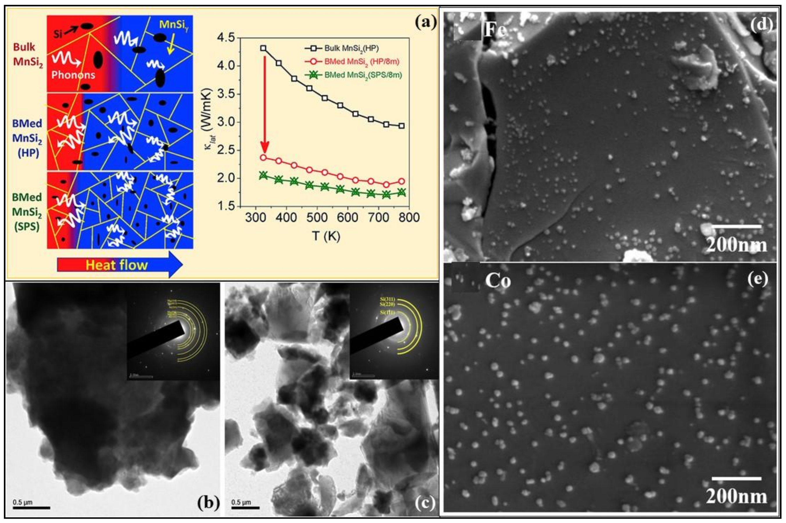
  79. Kim, G.; Kim, H.-S.; Lee, H.S.; Kim, J.; Lee, K.H.; Roh, J.W.; Lee, W. Synchronized enhancement of thermoelectric properties of higher manganese silicide by introducing Fe and Co nanoparticles. Nano Energy 2020, 72, 104698. [Google Scholar] [CrossRef]
  80. Li, Z.; Dong, J.-F.; Sun, F.-H.; Hirono, S.; Li, J.-F. Significant Enhancement of the Thermoelectric Performance of Higher Manganese Silicide by Incorporating MnTe Nanophase Derived from Te Nanowire. Chem. Mater. 2017, 29, 7378–7389. [Google Scholar] [CrossRef]
  81. Migas, D.; Shaposhnikov, V.; Filonov, A.; Borisenko, V.; Dorozhkin, N. Ab initio study of the band structures of different phases of higher manganese silicides. Phys. Rev. B 2008, 77, 075205. [Google Scholar] [CrossRef]
  82. Yamamoto, A.; Ghodke, S.; Miyazaki, H.; Inukai, M.; Nishino, Y.; Matsunami, M.; Takeuchi, T. Thermoelectric properties of supersaturated Re solid solution of higher manganese silicides. Jpn. J. Appl. Phys. 2016, 55, 020301. [Google Scholar] [CrossRef]
  83. Ghodke, S.; Hiroishi, N.; Yamamoto, A.; Ikuta, H.; Matsunami, M.; Takeuchi, T. Enhanced Thermoelectric Properties of W-and Fe-Substituted MnSi γ. J. Electron. Mater. 2016, 45, 5279–5284. [Google Scholar] [CrossRef]
  84. Liu, W.-D.; Chen, Z.-G.; Zou, J. Eco-Friendly Higher Manganese Silicide Thermoelectric Materials: Progress and Future Challenges. Adv. Energy Mater. 2018, 8, 1800056. [Google Scholar] [CrossRef]
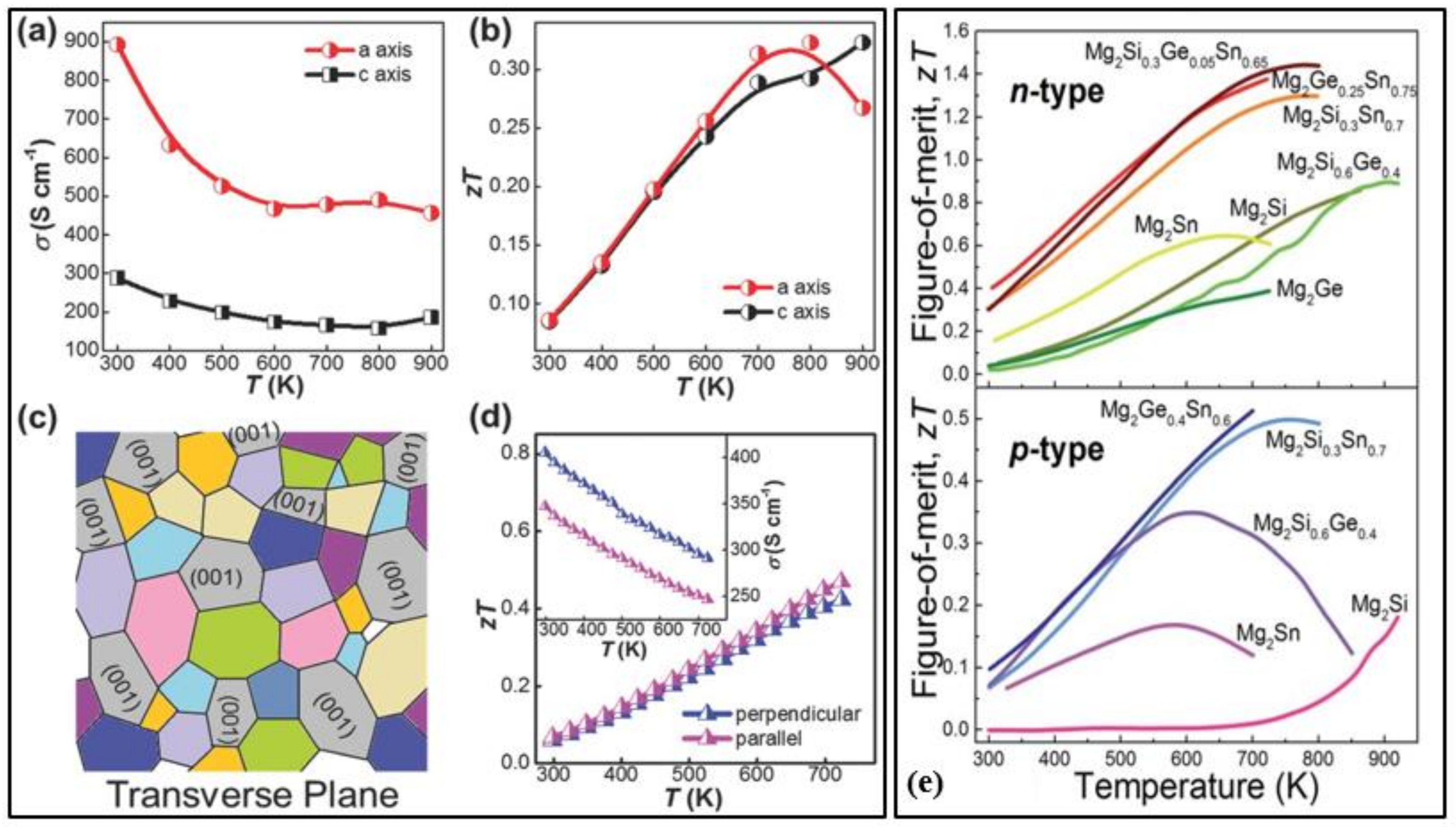
  85. Santos, R.; Yamini, S.A.; Dou, S.X. Recent progress in magnesium-based thermoelectric materials. J. Mater. Chem. A 2018, 6, 3328–3341. [Google Scholar] [CrossRef] [Green Version]
  86. Zaitsev, V.K.; Fedorov, M.I.; Gurieva, E.A.; Eremin, I.S.; Konstantinov, P.P.; Samunin, A.Y.; Vedernikov, M.V. Highly effective Mg2Si1−xSnx thermoelectrics. Phys. Rev. B 2006, 74, 045207. [Google Scholar] [CrossRef]
  87. Liu, W.; Tan, X.; Yin, K.; Liu, H.; Tang, X.; Shi, J.; Zhang, Q.; Uher, C. Convergence of conduction bands as a means of enhancing thermoelectric performance of n-type Mg2Si1−xSnx solid solutions. Phys. Rev. Lett. 2012, 108, 166601. [Google Scholar] [CrossRef] [Green Version]
  88. Sankhla, A.; Patil, A.; Kamila, H.; Yasseri, M.; Farahi, N.; Mueller, E.; De Boor, J. Mechanical Alloying of Optimized Mg2(Si,Sn) Solid Solutions: Understanding Phase Evolution and Tuning Synthesis Parameters for Thermoelectric Applications. ACS Appl. Energy Mater. 2018, 1, 531–542. [Google Scholar] [CrossRef] [Green Version]
  89. Dasgupta, T.; Umarji, A. Role of milling parameters and impurity on the thermoelectric properties of mechanically alloyed chromium silicide. J. Alloys Compd. 2008, 461, 292–297. [Google Scholar] [CrossRef]
  90. Upadhyay, N.K.; Kumaraswamidhas, L.; Dhar, A. Significant enhancement in thermoelectric performance of bulk CrSi2 employing quasi-binary solid solution CrSi2/MnSi1.73. Mater. Lett. 2020, 265, 127388. [Google Scholar] [CrossRef]
  91. Mikami, M.; Kinemuchi, Y. Microstructure and thermoelectric properties of WSi2-added CrSi2 composite. J. Alloys Compd. 2017, 690, 652–657. [Google Scholar] [CrossRef]
  92. Upadhyay, N.K.; Kumaraswamidhas, L.; Gahtori, B.; Bathula, S.; Muthiah, S.; Shyam, R.; Chauhan, N.S.; Bhardwaj, R.; Dhar, A. Enhancement in thermoelectric performance of bulk CrSi2 dispersed with nanostructured SiGe nanoinclusions. J. Alloys Compd. 2018, 765, 412–417. [Google Scholar] [CrossRef]
  93. Upadhyay, N.K.; Kumaraswamidhas, L.; Gahtori, B.; Muthaiah, S.; Bathula, S.; Shyam, R.; Dhar, A. Facile synthesis of earth-abundant and non-toxic p-type Si96B4/SiCp nanocomposites with enhanced thermoelectric performance. Mater. Sci. Semicond. Process. 2018, 75, 234–238. [Google Scholar] [CrossRef]
  94. Ren, G.; Lan, J.; Zeng, C.; Liu, Y.; Zhan, B.; Butt, S.; Lin, Y.-H.; Nan, C.-W. High Performance Oxides-Based Thermoelectric Materials. JOM 2015, 67, 211–221. [Google Scholar] [CrossRef]
  95. Zevalkink, A.; Toberer, E.S.; Zeier, W.G.; Flage-Larsen, E.; Snyder, G.J. Ca3AlSb3: An inexpensive, non-toxic thermoelectric material for waste heat recovery. Energy Environ. Sci. 2011, 4, 510–518. [Google Scholar] [CrossRef] [Green Version]
  96. Thunis, G.; Rignanese, G.-M.; Hautier, G. Electronic Transport Properties of Thermoelectric Zintl Compounds Ca5Al2Sb6 and Ca3AlSb3: An ab Initio Study. Master’s Thesis, Université Catholique de Louvain, Louvain-la-Neuve, Belgium, 2016. [Google Scholar]
  97. Toberer, E.S.; Zevalkink, A.; Crisosto, N.; Snyder, G.J. The Zintl Compound Ca5Al2Sb6 for Low-Cost Thermoelectric Power Generation. Adv. Funct. Mater. 2010, 20, 4375–4380. [Google Scholar] [CrossRef]
  98. Zhang, J.; Song, L.; Mamakhel, A.; Jørgensen, M.R.V.; Iversen, B.B. High-Performance Low-Cost n-Type Se-Doped Mg3Sb2-Based Zintl Compounds for Thermoelectric Application. Chem. Mater. 2017, 29, 5371–5383. [Google Scholar] [CrossRef] [Green Version]
  99. Bhardwaj, A.; Rajput, A.S.; Shukla, A.K.; Pulikkotil, J.J.; Srivastava, A.K.; Dhar, A.; Gupta, G.; Auluck, S.; Misra, D.K.; Budhani, R.C. Mg3Sb2-based Zintl compound: A non-toxic, inexpensive and abundant thermoelectric material for power generation. RSC Adv. 2013, 3, 8504–8516. [Google Scholar] [CrossRef]
  100. Shuai, J.; Wang, Y.; Kim, H.S.; Liu, Z.; Sun, J.; Chen, S.; Sui, J.; Ren, Z. Thermoelectric properties of Na-doped Zintl compound: Mg3−xNaxSb2. Acta Mater. 2015, 93, 187–193. [Google Scholar] [CrossRef] [Green Version]
Figure 1. (a) Recent progress of figure of merit (ZTmax) of Earth-abundant low-toxic thermoelectric materials; Low-temperature thermoelectric materials (copper iodide and its alloys), Intermediate and high-temperature thermoelectric materials (copper sulfides, silicides, Zintl compounds, and their alloys) from the year 2008–2020. The temperatures at which the maximum ZT recorded is mentioned in the bar-charts. (b) silicides, (c) Zintl compounds, (d) copper sulfides, (e) copper iodide (Tables 1 and 2).
Nanomaterials 11 00895 g001
Figure 2. (a) Transmittance spectra of copper iodide thin film deposited of glass (thickness of 300 nm), Reproduced with permission from [9]. Copyright © 2017, Nature Communications, (b) Room temperature power factors of copper iodide at different annealing temperatures, Reproduced with permission from [10]. Copyright © 2018, Wiley Online Library, (c) SEM image of nanostructured CuI synthesized using vapour iodination and thermal evaporation, Reproduced with permission from [11]. Copyright © 2018, Scientific Reports Nature. (d) A 10 × 10 cm2 Kapton-based copper iodide (CuI) and gallium-doped zinc oxide (GZO) based thermoelectric generator prototype, Reproduced with permission from [12]. Copyright © 2019, Royal Society of Chemistry, (e) Schematic representation of transparent flexible copper iodide thin-film thermoelectric generator (p-type material is CuI and n-type material is GZO) with 17 p-n modules connected in series with indium tin oxide (ITO) using platinum wire, Reproduced with permission from [12]. Copyright © 2019, Royal Society of Chemistry, (f) Illustration of CuI (doped with terbium) single nanocrystal, Reproduced with permission from [13]. Copyright © 2020, Elsevier.
Nanomaterials 11 00895 g002
Figure 5. Temperature-dependent thermoelectric performance of the three Bi13S18I2 samples (bulk, nano & nano with 2% BiCl3) (a) Electrical conductivity, (b) Hall Carrier concentration, (c) Seebeck Coefficient, (d) Power Factor, (e) Thermal Conductivity, (f) Figure of merit (ZT), Reproduced with permission [49]. Copyright © 2018, Wiley Online Library.
Nanomaterials 11 00895 g005
Figure 8. (a) Temperature dependence of figure of merit for various Mg3Sb2-based Zintl compounds: Silver doped Mg3Sb2, sodium doped Mg3Sb2, Mg3.07Sb1.5Bi0.48Se0.02, Mg3Sb1.48Bi0.48Te0.04, Mg3Sb1.8Bi0.2, Mg3Sb2, Reproduced with permission from [98] Copyright © 2017, ACS Publications. (b,c) SEM of Ca4.75Na0.25Al2Sb6 with 98% theoretical density value (polished surfaces (b) and fracture surfaces (c)) and grains as large as 50 µm in diameter are revealed, Reproduced with permission from [97] Copyright © 2010, Wiley Online Library.
Nanomaterials 11 00895 g008
Table 1. Prominent nanostructured copper-iodide (CuI) alloys/composites thermoelectric materials.
Sr.noMaterialOperating
Temperature (K)
Synthesis Techniqueσ * (Scm−1)K *
(Wm−1K−1)
Seebeck Coefficient (µVK−1)PF *
(S2σ/µWm−1K−2)
ZT *maxYear/
Reference
1p-type CuI300SputteringN/A0.552373750.212017 [9]
2p-type CuI353Simple Synthesis
Vacuum Annealing
N/AN/A431160N/A2018 [10]
3p-type CuI
n-type GZO
300Sputtering
Thermal evaporation
Solid deposition
Vapor method
110N/A2064700.222018 [11]
4p-type CuI
n-type GZO
373Resistive thermal
evaporation
110
142
0.48
2.17
206.0
−60
470
500
0.29
0.07
2019 [12]
5CuI:Tb (0.05 mol%) NP *430Hydraulic pressing
Vacuum annealing
~500~0.5~7003500.282020 [13]
* Nomenclature: NP: nanoparticles; NS: nanosheets; σ: electrical conductivity; k: thermal conductivity; PF: power factor; ZT: the figure of merit.
Table 3. The maximum figure of merit ZT for various oxide-based thermoelectric materials [94].
Type of Thermoelectric MaterialMax ZT
n-typeZnO-based0.54 at 1000 K
SrTiO3-based0.37 at 973 K
In2O3-based0.7 at 1073 K
p-typeCa3Co4O9-based0.4 at 975 K
BiCuSeO-based1.4 at 923 K
NiO-based0.075 at 1000 K
Publisher’s Note: MDPI stays neutral with regard to jurisdictional claims in published maps and institutional affiliations.

