Article

Interface Optimization and Transport Modulation of Sm2O3/InP Metal Oxide Semiconductor Capacitors with Atomic Layer Deposition-Derived Laminated Interlayer

1
School of Materials Science and Engineering, Anhui University, Hefei 230601, China
2
School of Physics and Optoelectronics Engineering, Anhui University, Hefei 230601, China
3
School of Integration Circuits, Anhui University, Hefei 230601, China
4
School of Mathematical Information, Shaoxing University, Shaoxing 312000, China
*
Authors to whom correspondence should be addressed.
Nanomaterials 2021, 11(12), 3443; https://doi.org/10.3390/nano11123443
Submission received: 14 November 2021 / Revised: 13 December 2021 / Accepted: 16 December 2021 / Published: 19 December 2021

Abstract

:
In this paper, the effect of atomic layer deposition-derived laminated interlayer on the interface chemistry and transport characteristics of sputtering-deposited Sm2O3/InP gate stacks have been investigated systematically. Based on X-ray photoelectron spectroscopy (XPS) measurements, it can be noted that ALD-derived Al2O3 interface passivation layer significantly prevents the appearance of substrate diffusion oxides and substantially optimizes gate dielectric performance. The leakage current experimental results confirm that the Sm2O3/Al2O3/InP stacked gate dielectric structure exhibits a lower leakage current density than the other samples, reaching a value of 2.87 × 10⁻⁶ A/cm2. In addition, conductivity analysis shows that high-quality metal oxide semiconductor capacitors based on Sm2O3/Al2O3/InP gate stacks have the lowest interfacial density of states (Dit) value of 1.05 × 1013 cm−2 eV−1. The conduction mechanisms of the InP-based MOS capacitors at low temperatures are not yet known, and to further explore the electron transport in InP-based MOS capacitors with different stacked gate dielectric structures, we placed samples for leakage current measurements at low varying temperatures (77–227 K). Based on the measurement results, Sm2O3/Al2O3/InP stacked gate dielectric is a promising candidate for InP-based metal oxide semiconductor field-effect-transistor devices (MOSFET) in the future.

1. Introduction

As the integration of IC continues to increase, CMOS feature sizes will also continue to decrease in order to reduce the cost of individual transistors, increase the switching speed of transistors, and reduce the power consumption of the circuit. As the feature size of CMOS devices continues to decrease, it will also cause the SiO2 gate dielectric and Si substrate used in conventional processes to decrease in size as well. When the size is smaller than a certain limit, the gate leakage current will grow exponentially, while the device will not operate properly due to the laws of quantum physics [1,2]. The use of high-k materials for the replacement of SiO2 gate dielectrics is an option that has been shown to be feasible [3]. Among these high k materials, samarium oxide (Sm2O3) is considered as the next potential gate dielectric due to its high dielectric constant (~15) [4], sufficiently large band gap (5.1 eV) [5], low hygroscopicity, and high chemical and thermal stability [6]. Coulomb scattering and phonon scattering at the interface between the high-k gate dielectric and the channel material lead to a significant reduction in channel mobility, which severely affects the further increase in the speed of CMOS logic devices. Selecting channel materials with high mobility is an effective way to solve this problem [7]. Compared with conventional Si-based material CMOS devices, III-V group semiconductors have advantages due to their large switching speed and small dynamic power consumption [8]. Among the group III-V semiconductors, InP has received more attention due to its higher carrier mobility and smaller band gap [9].
However, InP is prone to the formation of interfacial defects, which can limit the operating performance of the device [10]. Also, a surface with many chemical impurities can have a considerable impact on the performance of InP MOS capacitors [11]. High Dit leads to the frequency dispersion of the Fermi energy level pegging and capacitance, which also prevents the formation of inverse or accumulation layers in CMOS devices [12].
Different InP surface passivation methods have been investigated for a long time, including low-temperature processes [13], ozone treatment [14], chemical etching [15], and sulfide solution passivation [16,17]. A great deal of work has also been devoted to atomic layer deposition (ALD) passivation layers to modulate the InP interface [18]. It has been demonstrated that ALD-derived Al2O3 films can effectively suppress the interfacial diffusion from the substrate to the high-k films. More importantly, the operating temperature can be kept low (~200 °C) when the Al2O3 film is on the passivated substrate surface. There are previous reports confirming that the insertion of Al2O3 between the high-k gate dielectric and GaAs can improve the thermal stability. However, even in the presence of an Al2O3 passivation layer to improve the interface, the diffusion of In and P elements into the gate dielectric still has an impact on the electrical characteristics of the device when fabricating InP MOS capacitors. R. V. Galatage et al. reported that the In-O and P-O states at the interface lead to a degradation of the electrical characteristics [19]. Their results also demonstrated the effectiveness of ALD-derived Al2O3 passivation layers between the gate dielectric and the InP substrate. Chee-Hong An et al. systematically analyzed that Al2O3 can inhibit dissociation and reactant diffusion in InP substrates [20]. However, the effect of the position of the Al2O3 passivation layer on the electrical properties and interfacial bonding state of InP MOS devices has not been reported systematically.
In this work, we deposited Sm2O3 films by magnetron sputtering and obtained Al2O3 passivation layers by ALD equipment to fabricate three different gate stacks on InP substrates, corresponding to Al2O3/Sm2O3/InP, Al22O3/Sm2O3/Al2O3/InP, and Sm2O3/Al2O3/InP, respectively. X-ray photoelectron spectroscopy (XPS) and electrical measurements were used to investigate the effect of Al2O3 passivation position on the chemical composition and electrical parameters of the interface. In addition, the leakage current conduction mechanisms (CCMs) of InP-based MOS capacitors with three different laminated gate electrical stacks measured at room temperature and low temperature (77–227 K) were systematically investigated.

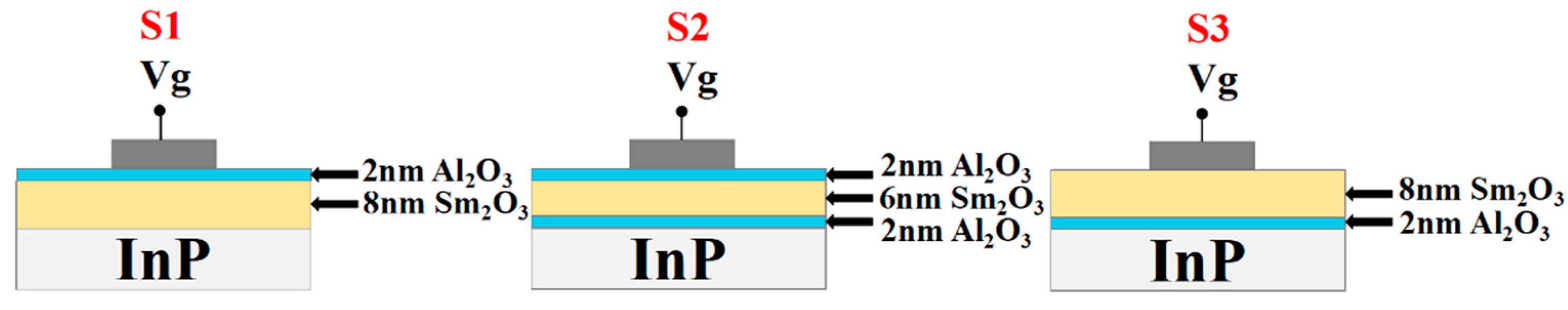
2. Materials and Methods

In this work, we chose sulfur-doped n-type InP wafers as the substrate for fabricating MOS capacitors. Before depositing the Sm2O3 gate dielectric, the wafers were subjected to a standard degreasing process by sequential immersion in ethanol and acetone for 5 min each. After that, the wafers were immersed in 20% ammonium sulfide solution for 15 min to remove the native oxides. Then, the wafers are rinsed with deionized water and then blown dry with high purity nitrogen gas. The cleaned wafers are transferred to an ALD system (MNT-PD100Oz-L6S1G2, MNT Micro and Nanotech). On the ALD process, plasma O2 and trimethylaluminum (TMA) were selected as the oxidant and aluminum metal precursor, and a 2 nm Al2O3 passivation layer was deposited on the InP substrate. The Al2O3 passivation layers were deposited by using 30 pulse cycles of plasma O2 precursors [O2(2s)/Ar purge (25s)] and 15 pulse cycles of trimethylaluminum (TMA) and plasma O2 [TMA (0.03s)/O2 2s/Ar purge (25s)], respectively. During this process, the chamber pressure and the deposition temperature were maintained at 35 Pa and 200 °C. After ALD Al2O3 passivation, the wafers were transferred to a sputtering chamber to deposit Sm2O3 gate dielectrics by sputtering samarium target with purity of 99.9%. When the chamber pressure was 0.8 Pa, Sm2O3 thin film was deposited under an Ar/O2 (50/10 sccm) atmosphere. To explore the electrical characteristics of Sm2O3/InP MOS capacitors with different stacking positions of Al2O3 passivation layers, a 200-μm-diameter Al electrode was deposited by thermal evaporation, while an aluminum electrode was grown on the back side to form an ohmic contact. Figure 1 demonstrates the schematics of InP-MOS capacitors based on different stacked gate dielectric structures. Sample S1 corresponds to Al2O3 (2 nm)/Sm2O3 (8 nm)/InP, sample S2 corresponds to Al2O3 (2 nm)/Sm2O3 (6 nm)/Al2O3 (2 nm)/InP, and sample S3 corresponds to Sm2O3 (8 nm)/Al2O3 (2 nm)/InP, respectively. By using the ESCALAB 250Xi system, XPS (X-ray photoelectron spectroscopy) measurements were performed at Al Ka (1486.7 eV) to investigate the interfacial chemical properties of the Sm2O3/InP gate stack and the chemical function of the Al2O3 passivation layer. Furthermore, the escape angle used in obtaining the XPS profiles is 50° and the corresponding probing depth is about 1–10 nm. Ultraviolet-visible spectroscopy (Shimadzu, UV-2550) was performed to obtain the samples’ optical band gap. The physical thickness of the above samples was extracted by using spectroscopic ellipsometry measurements (SANCO Inc., Shanghai, China, SC630) with the help of the Cauchy-Urbach model. The Cascade Probe Station was connected to the semiconductor analysis equipment (Agilent B1500A) for capacitance-voltage (C-V), transconductance-voltage (G-V), and leakage current-voltage (I-V) measurements at room temperature. For low temperature (77–227 K) leakage current testing, the Lake Shore Cryotronics Vacuum Probing Station was used.

3. Results and Discussion
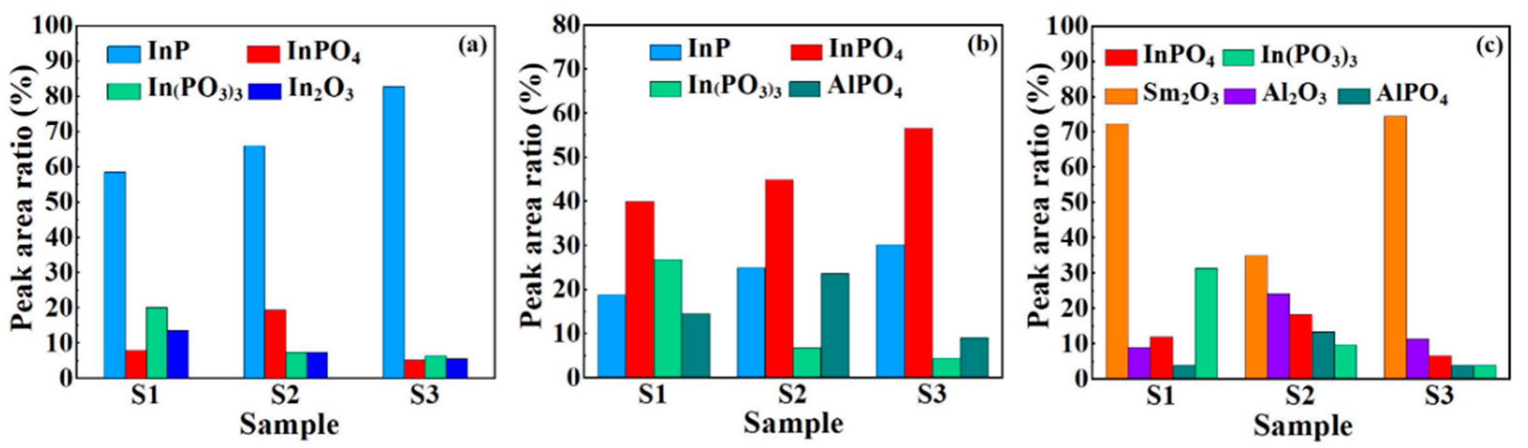
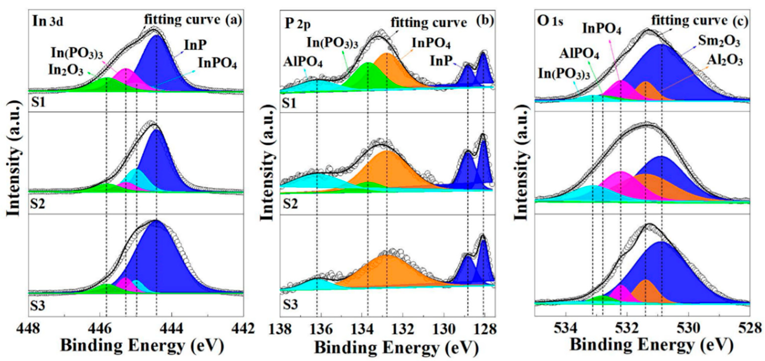
3.1. XPS Analyses

To evaluate the chemical bonding states of various stacked gate dielectrics, XPS measurements were carried out. Figure 2 displays the In 3d, P 2p, and O 1s XPS spectra of three samples with various stacked gate dielectrics. It can be noted that In 3d spectra can be deconvoluted into four components that represent the InP, InPO4, In(PO3)3, and In2O3, respectively. The relative intensity values of the different components have been extracted and are shown in Figure 3a. For S2 and S3, the contents of In(PO3)3 and In2O3 shows a decreasing trend, indicating that the ALD-derived Al2O3 passivation layers prior to Sm2O3 deposition can significantly prohibit the formation of In and P suboxides, which can be attributed to the interface cleaning function of plasma O2 [21]. Compared to S2, the peak areas of InPO4 corresponding to S1 and S3 remain approximate at about 7.89% and 5.20%, which is much lower than that of S2 (19.41%), indicating that double deposition of ALD-derived Al2O3 may accelerate the diffusion of oxygen in the substrate and the formation of indium phosphate. During the secondary deposition of Al2O3, more oxygen vacancies may generate, which can be ascribed to plasma O2 acting as an oxygen source, and promote the oxygen interdiffusion between Al2O3 passivation layers and the InP substrate. In(PO3)3 can react with In to produce InP and InPO4 using the following reaction Equation [22].
8In + 4In(PO3)3 → 3InP + 9InPO4
More importantly, sample S3 shows a tendency to decrease the content of In(PO3)3 and AlPO4 compared to sample S2, which can give a detailed illustration from the phenomenon of P 2p spectral changes. As shown in Figure 2b, it can be noted that P 2p spectra can be deconvoluted into four components, which represent InP, InPO4, In(PO3)3, and AlPO4, respectively. No P2O5 was detected in all samples, which can be attributed to the fact that gaseous P2O5 generated during the deposition can easily diffuse through the defects in the gate dielectric [22]. The peak area ratio of In(PO3)3 for S2 and S3 showed a significant decreasing trend compared to S1, indicating that Al2O3 prior to the deposition of Sm2O3 gate dielectric can inhibit the formation of P-O bound states and improve the interfacial quality. The detection of AlPO4 in P 2p spectra can be attributed to the reaction equation described below [23].
4Al + 7O2 + 2In(PO3)3 + 2InP → 4AlPO4 + 4InPO4
Based on the mentioned reaction above, it can be inferred that two depositions of Al2O3 passivation layers increase the formation of AlPO4, which is confirmed by the change in peak area ratio shown in Figure 3c. In order to systematically explore the interfacial chemistry of various stacked gate dielectrics, O 1s spectra were investigated and are shown in Figure 2c. O 1s spectra can be deconvoluted into Sm2O3, Al2O3, InPO4, In(PO3)3, and AlPO4. According to the reaction Equation (2), in the plasma O2 atmosphere, In(PO3)3 can react with O2 to produce AlPO4 and InPO4 and leads to the disappearance of In(PO3)3. In agreement with the previous In 3d and P 2p spectra, S1 has the largest In(PO3)3 content, leading to a decrease in interfacial quality and deterioration of electrical properties. Meanwhile, AlPO4 of S2 is the highest, originating from the second deposition of Al2O3. For S3 sample, the contents of InPO4, AlPO4, and In2O3 were significantly controlled, indicating that the addition of an ALD-derived Al2O3 layer prior to the deposition of Sm2O3 gate dielectric could reduce the generation of suboxides and improve the interfacial quality.

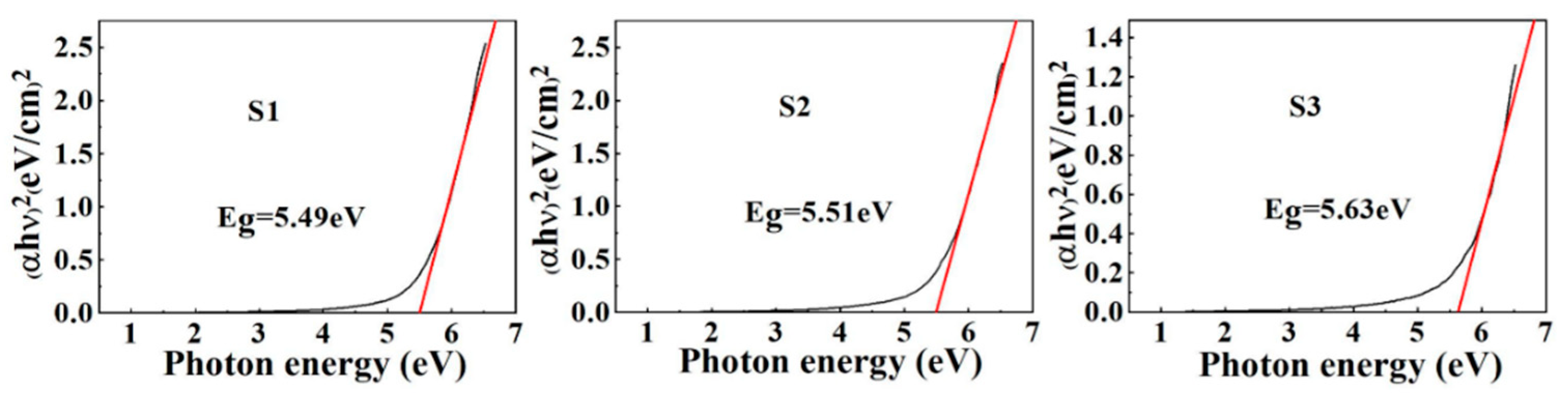
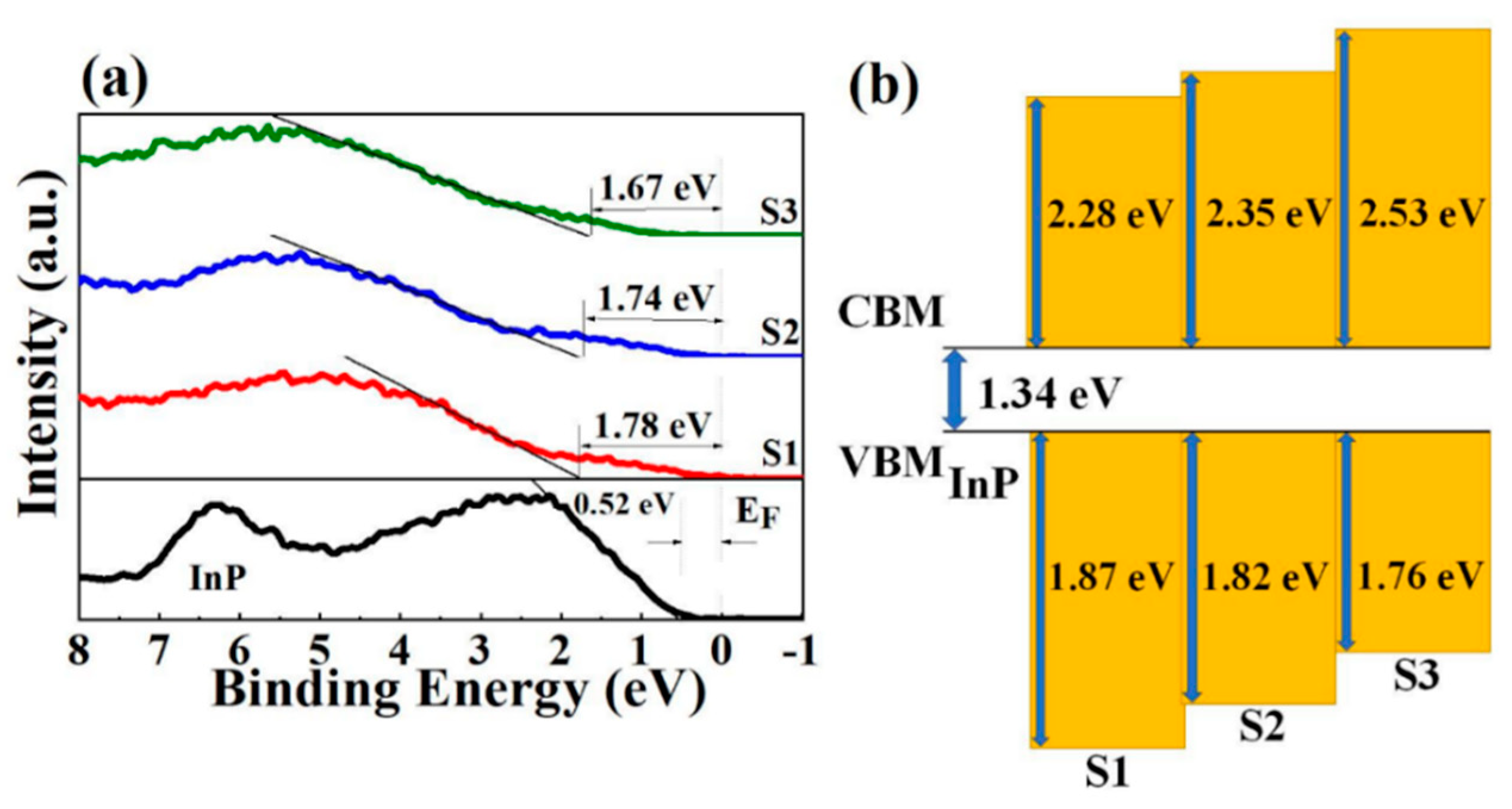
3.2. Band Alignment Characteristics

To assess the optical characteristics of the three various stacked gate dielectrics, UV-Vis spectroscopy was used to obtain the absorption spectra and the optical bandgap values (Figure 4) of samples S1, S2, and S3 were determined to be 5.49, 5.51, and 5.63 eV, respectively, based on the Tauc relationship [24]. Compared with pure Sm2O3 and pure Al2O3, the band gaps of three various stacked gate dielectrics showed a value balance [25]. Also, this section investigates the valence band maximum (VBM) of various stacked gate dielectrics, as the valence band alignment is crucial for assessing the interface quality. As shown in Figure 5a, the band gap values of InP substrates were derived from XPS measurements, while the valence bands of samples S1, S2, and S3 were deduced from the absorption spectra by linear extrapolation. Based on Kraut’s method [26], we also calculated the valence band shift ( E V ) to evaluate the valence band electronic structure of the samples. By using Sm 3d5/2 and In 3d core-level spectra, the E V of high-k/InP gate stacks was determined based on the following formula:
E V = ( E In   3 d E V ) InP ( E Sm   3 d E V ) high - k ( E In   3 d E Sm   3 d ) high - k / InP
where EIn 3d (InP) and ESm 3d (high-k) corresponding to the core-level positions are extracted to be 445.8 and 1084.3 eV. In addition, the Ev (InP) and Ev (high-k) represent the VBM (Valence-Band Maximum) of the bulk materials. The values of ΔEv are calculated as 1.87, 1.82, and 1.76 eV, respectively, based on the binding energy difference in the high-k/InP structure. Meanwhile, the value of the conduction band offset (ΔEc) is obtained by subtracting the extracted ΔEv and the band gap of the InP (1.34 eV) from the band gap of dielectric layers [27].
Δ E C   ( high - k / InP ) = E g   ( high - k ) Δ E V ( High - k / InP ) E g ( InP )
As shown in Figure 5b, the ΔEc values for the three samples were calculated as 2.28, 2.35, and 2.53 eV. According to previous reports in the literature, ΔEc is related with the tunneling leakage current. The higher ΔEc indicates that the leakage current of the Sm2O3/Al2O3/InP samples is smaller.

3.3. Electrical Properties of InP-MOS Capacitors

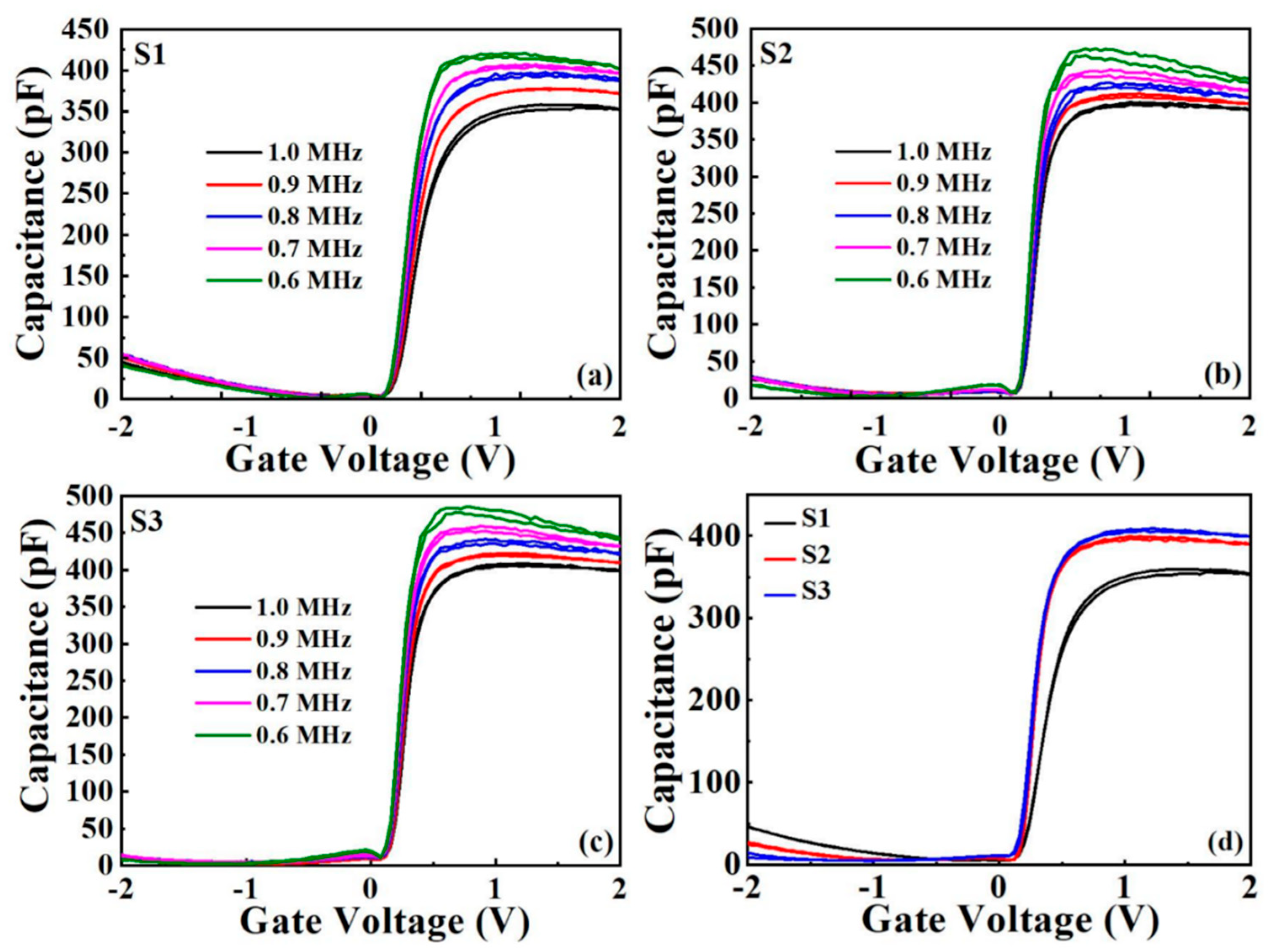
3.3.1. Capacitance-Voltage Measurements

The frequency dependent capacitance-voltage curves of sample S1, S2, and S3 with double sweep mode are shown in Figure 6a–c. When the frequency increases, all samples show a decreased accumulation capacitance.
Meantime, at high frequency conditions, the series resistance will deviate from the predetermined theoretical value due to the disappearance of the interface trap charge. On the contrary, at low frequencies, when the oxide capacitance (Cox) connects with the space charge capacitance (Csc), the value of the accumulation region increases with the series resistance due to the interface state showing frequency-dependent properties [28,29,30].
The decrease in the accumulation capacitance can be attributed to the fact that the interfacial traps do not have enough time to respond to the voltage frequency [30]. The maximum accumulation capacitance and minimum hysteresis voltage were observed in the S3 sample, indicating that the Al2O3 passivation layer suppressed the appearance of In and P oxides and the formation of low-K interfacial layers. To evaluate the interface quality, important electrical parameters such as equivalent oxide thickness (EOT), dielectric constant (k), flat band voltage (Vfb), hysteresis voltage (ΔVfb), oxidation charge density (Qox), and boundary trapped oxide charge density (Nbt) were extracted from the test curves, and these data are presented in Table 1. The variation of Vfb depends on the values of oxide capacitance and bulk oxide charge [31]. The k values corresponding to samples S1, S2, and S3 are calculated to be 12.96, 14.39, and 14.75, which are consistent with the previous investigation [4].
A small Vfb of 0.19 V was observed for sample S3. This phenomenon can be explained by the following statement: electrons are easily captured by oxygen vacancies to form negatively charged interstitial oxygen atoms [32] and as fewer oxygen vacancies exist at the interface, the smaller the positive flat voltage required to maintain the band unbent [33]. Also, the hysteresis voltage depends on the boundary trap caused by the intermixing of the high K layer and the interfacial layer [34]. The value of the hysteresis voltage reaches a minimum (1.55 mV) for S3, indicating that the boundary trapping charge becomes weaker after the insertion of Al2O3 between the gate dielectric and the substrate. The Qox and Nbt values were calculated from the obtained Vfb and ΔVfb values by the following equations [35].
Q o x = C max ( v f b φ m s ) q A
N b t = C max V f b q A
where φ m s is the contact potential difference between Al electrode and InP substrate, q is the electronic charge, and A is the Al electrode areas. According to Table 1, it can be noticed that S3 has the lowest Qox and Nbt, which implies the reduction of interfacial trap defects and the optimization of interfacial properties.

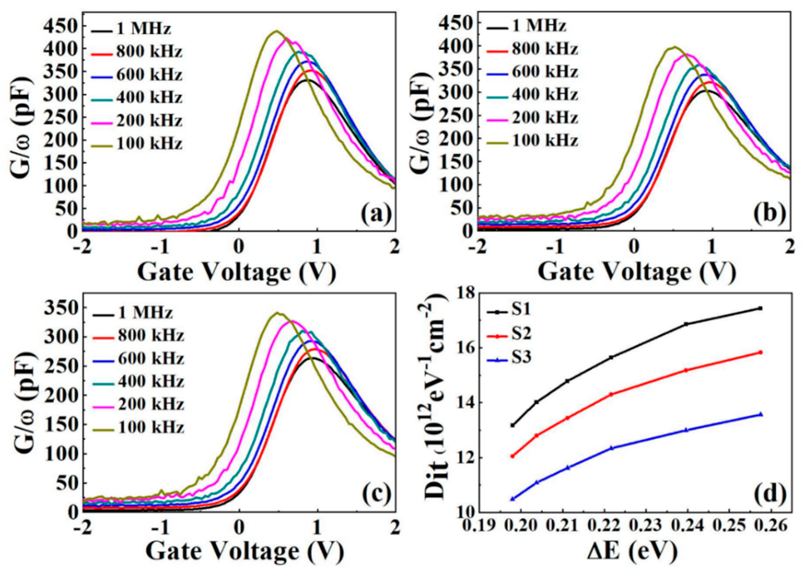
3.3.2. Conductivity-Voltage Measurements
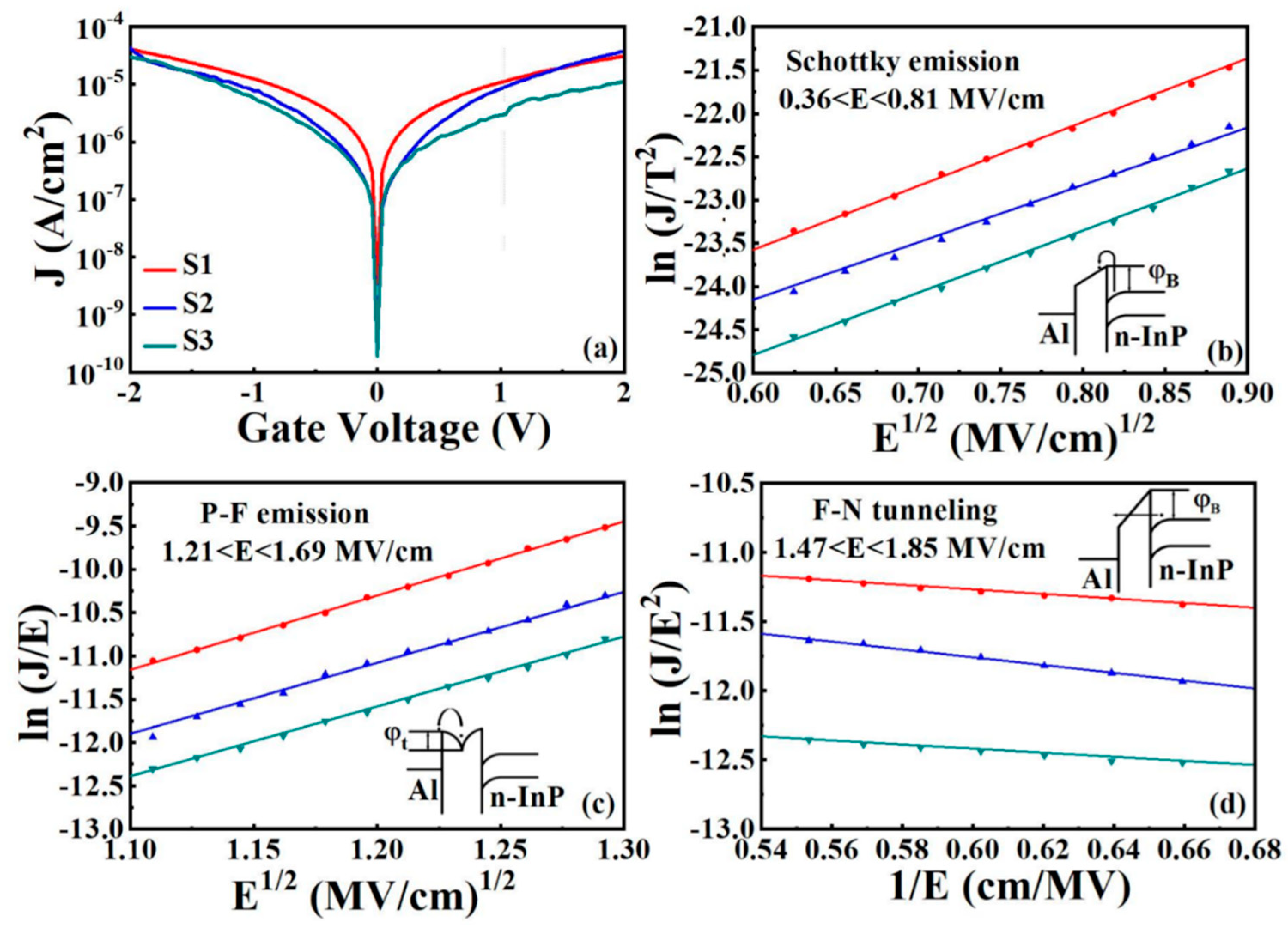
Moreover, to quantify the interface defect distribution for all samples, the interface state density (Dit) has been extracted by the conductivity-voltage measurements with frequencies varying from 100 kHz to 1 MHz. Dit is related to the parallel interfacial trap capacitance (Cit) and parallel conductivity (G). At the same time, Cit can be related by the following equation. Cit = q Dit, while the condition is that the position of the energy level does not change Dit. The basic principle of conductivity measurements is to analyze the losses due to the diversity of charge states at the trap level. Near the Fermi level, the synchronous conductivity occupancy is mobilized by the interfacial traps to produce a regular variation. The maximum loss occurs when the interface trap is resonantly shifted with the applied AC signal ( ω τ = 1). The response time of the characteristic trap changes the frequency, τ = 2 π / ω . The capture and emission rates from Shockley-Redhall theory modulate the response time [36]:
τ = e x p [ E / k B T ] σ v t h D d o s
where there is an energy difference E between the trap level ET and the edge of the majority carrier band, v t h is the majority carrier being thermally activated to obtain the average velocity, Ddos is the effective density of states of the majority carrier band, k B is the Boltzmann constant, and T is the temperature [37]. The curves between conductivity (G/ω) and gate voltage for all samples are shown in Figure 7a–c. The apparent shift of the conductivity peak proves the validity of the Fermi-level shift and confirms the existence of the Fermi-level deconvolution effect [38]. Assuming that the underlying surface oscillations can be neglected, the value of Dit is inferred using the normalized parallel conductivity peak ( G P / ω ) m a x [39].
D i t 2.5 A q ( G p ω ) m a x
where A is the device area. It is necessary to confirm the transformation law between the band bending potential of the energy location ET and the trap energy level distribution. Furthermore, the values of ET can be determined by the frequency of ( G P / ω ) m a x , where Equation (8) is used to calculate Dit and to correspond its value to E [40].
E = ( E C E T ) = k B T q I n ( σ v D d o s 2 π f m a x )
Figure 7d shows the variation of Dit for the three samples. With the increase of ΔE, the value of Dit shows an increasing trend. However, S3 possesses a lower density of interfacial states compared to S1 and S2, which indicates that the insertion of an Al2O3 passivation layer between the Sm2O3 gate dielectric and the InP substrate can suppress the formation of In and P suboxides and improve the quality of MOS capacitors.
We compared some of the data obtained from this work with some previously published work. As can be seen in Table 2, the Sm2O3 dielectric has a smaller leakage current density than TiO2 and HfO2, indicating that the Sm2O3 stacked gate dielectric has a larger conduction band shift, resulting in an increased barrier height and thus a reduced leakage current density. The Sm2O3 stacked gate dielectric has the smallest hysteresis value, indicating that the trapped charge in the gate dielectric is not very sensitive to the frequency response of the voltage, and will trap fewer electrons to keep the energy band from being bent, while the device maintains a consistent response to different test voltages in the antipattern region. In the interface state density, it is smaller than HfO2 as the gate dielectric directly deposited in InP, but it seems to be higher than TiO2 gate dielectric, considering the different testing methods, the interface state density of the current work is obtained directly by conductivity method with accuracy, the previous work is by C–V curve, there may be some differences.

3.3.3. JV Analyses and Conduction Mechanisms at Room Temperature
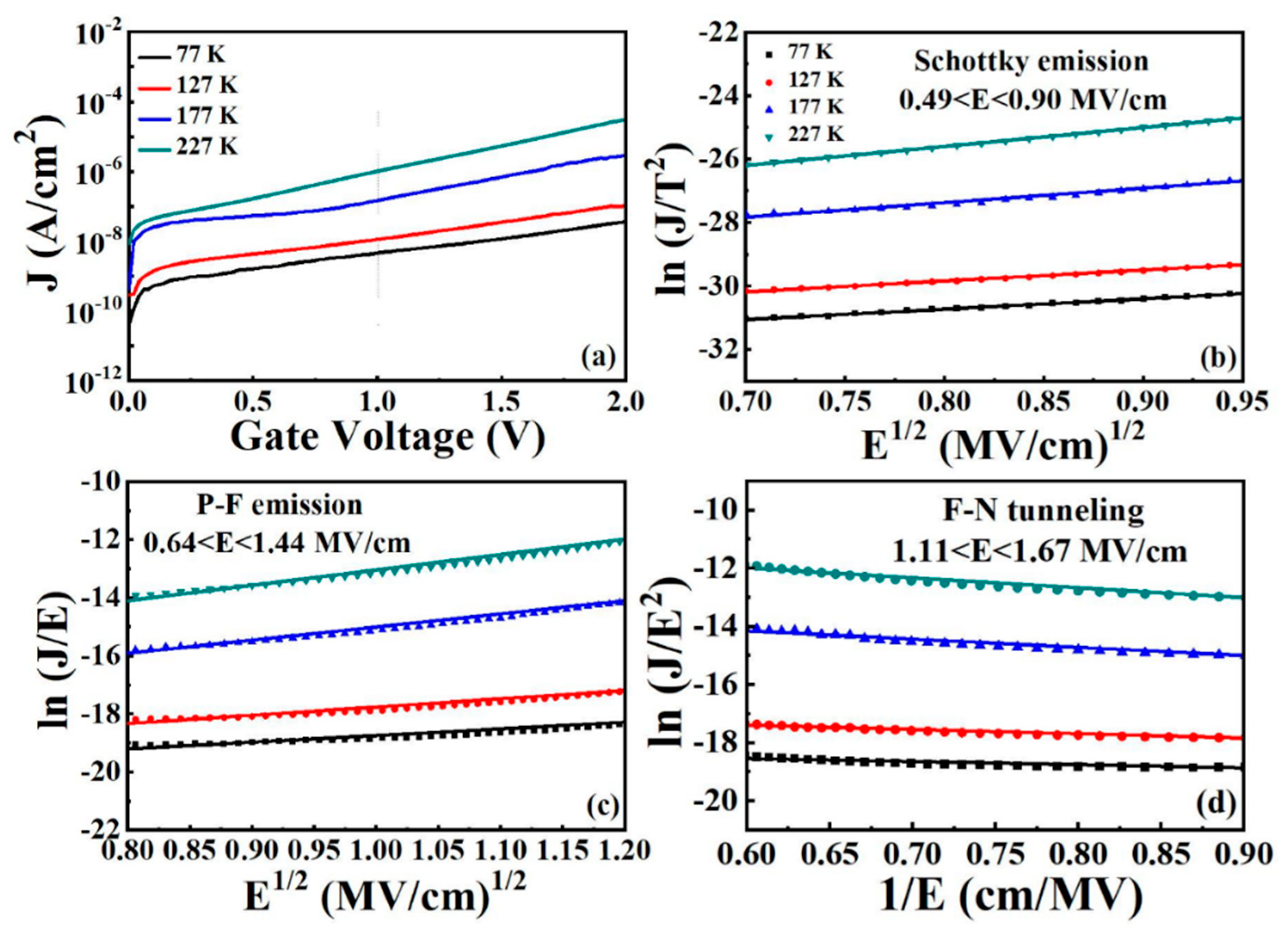
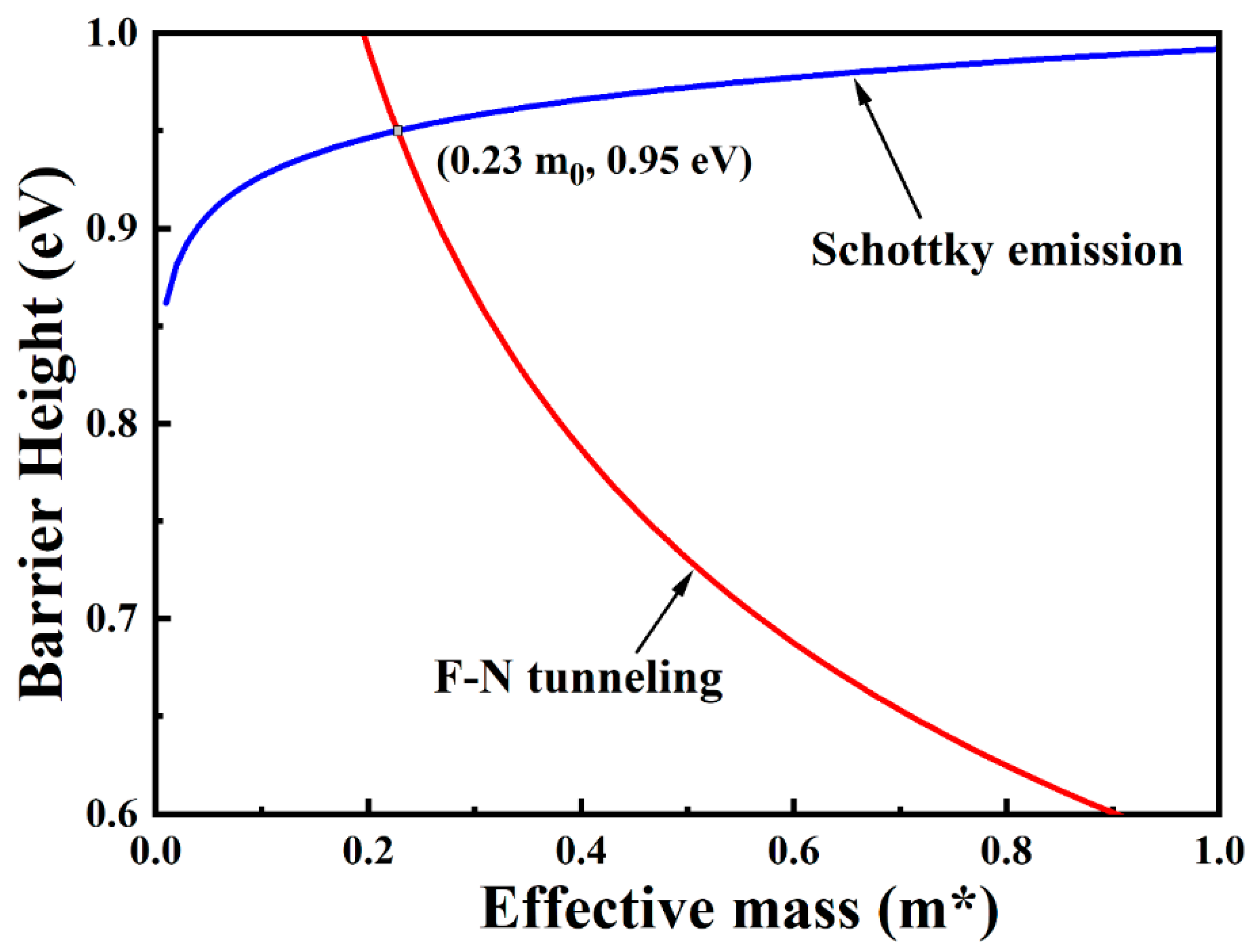
Figure 8a shows the leakage current characteristics of all samples measured at room temperature. The leakage current density (J) values for S1, S2, and S3 at 1 V are 1.07 × 10⁻⁵, 8.42 × 10⁻⁶, and 2.87 × 10⁻⁶ A/cm2, respectively. It can be seen that S1 has a higher leakage current density, which can be attributed to larger interface traps and the border traps that deteriorate the interface quality and degrade the device performance [44]. For the S3 sample, the minimum leakage current density has been observed, which is due to the higher ΔEc and the suppressed tunneling in the Sm2O3/Al2O3/InP gate stack [45].
To investigate the leakage current characteristics of various stacked gate dielectrics, we systematically studied three different current conduction mechanisms (CCMs) under substrate injection, as shown in Figure 8b–d. The extracted important electrical parameters are listed in Table 3.
Schottky emission (SE) is a typical type of thermal ionization emission in which charges gain energy to overcome barriers to migration into the dielectric. The standard SE can be described as [46]:
J S E = A * T 2 e x p [ q ( φ B q E / 4 π ε 0 ε r ) k B T ]
A * = 4 π q k B 2 m o x * h 3 = 120 m o x * m 0
where A* is the effective Richardson constant, the free electron mass and the effective mass of electrons in the gate dielectric correspond to mo and mox*, E is the electric field, q φ B is the Schottky barrier height, and εo and εr represent the vacuum dielectric constant and the optical dielectric constant, respectively [47]. It is observed in Figure 8b that at lower electric fields (0.36–0.81 MV/cm), there is a good linear relationship between ln(J/T2) and E1/2 for S1, S2, and S3. The slope of the SE diagram is denoted as q 3 / 4 π ε 0 ε r / k B T . The fitted εr and the refractive index n (n = εr1/2) for S1, S2, and S3 are (4, 2), (4.96, 2.23), and (4.23, 2.06), respectively. All the fits are consistent with the previously reported values [48], revealing that CCM (current conduction mechanism) at room temperature is dominated by SE emission in the low electric field region.
The Poole–Frenkel (PF) emission can be ascribed to the thermally excited electrons obtaining sufficient energy to escape from traps into the conduction band of the dielectric at a higher electric field, which can be expressed by the following formula [49]:
J P F = A E   e x p [ q ( φ t q E / π ε 0 ε o x ) k B T ]
where A represents a constant, the trap energy level of the conduction band corresponds to φ t , and ε o x represents the dielectric constant. According to the previous theory, ln(J/E) should have a good proportionality with E1/2, as shown in Figure 8c. The εox extracted from the slope of the fitted line for all samples was calculated as 11.90, 13.01, and 13.41, which is in agreement with the reported reference [4]. It can be concluded that at higher electric fields (1.21–1.69 MV/cm), the PF emission dominates the CCM of all samples. Also, the value of the trap energy level ( φ t ) can be extracted based on the intercept point of the fitted curve described as l n B q φ t k B T . As shown in Figure 8c, the calculated values of φ t are 0.53, 0.54, and 0.55 eV, corresponding to S1, S2, and S3. S3 has the largest φ t value in the three samples, indicating that the electrons obtain more energy to cross the trap, leading to present the smallest leakage current density in the S3 sample.
The high-field dependent conduction mechanism is represented by Fowler-Nordheim tunneling, which is manifested by the fact that the insulating layer can be penetrated by electrons, which enter the conduction band of the gate dielectric in a high electric field. The leakage current density is linked to other parameters of Fowler-Nordheim (FN) tunneling and is described by the following Equation [46]:
J F N = q 3 E 2 16 π 2 φ o x   e x p [ 4 2 m T * φ B 3 / 2 3 q E ]
where φ o x is oxide barrier height; m T * is the tunneling effective electron mass in the gate oxide film, and the other notations remain unchanged from the previous definitions. Figure 8d shows the curve of ln(J/E2) versus 1/E. The slope of the linear fit for the above samples shows an increase in current with increasing electric field, indicating that at high electric fields (1.47–1.85 MV/cm), all three samples are consistent with the FN tunneling conduction mechanism. Based on the previous analysis, it can be concluded that all samples are dominated by three main conduction mechanisms. In the lower electric fields, SE emission dominates, however, in the higher electric fields, PF emission dominates together with FN tunneling.

3.3.4. Low Temperature JV Analyses and Conduction Mechanisms

To investigate the variation of CCMs in Sm2O3/Al2O3/InP MOS capacitor, low temperature (77–227 K) measurements were performed. The leakage current densities of Sm2O3/Al2O3/InP MOS capacitors measured at 1 V were extracted as 4.64 × 10⁻⁹, 1.48 × 10⁻⁸, 1.13 × 10⁻⁷, and 1.02 × 10⁻⁶ A/cm2, corresponding to the temperature range of 77–227 K, respectively. By observing the leakage current densities at different temperatures, the Sm2O3/Al2O3/InP gate stack exhibits nearly three orders of magnitude lower leakage current density at 77 K than that measured at room temperature, indicating that the low temperature is favorable for the MOS capacitor to exhibit optimized JV characteristics. Figure 9b–d show the variation of the CCM under substrate injection along with the temperature trend. The extracted important electrical parameters are listed in Table 4. Figure 9b shows the fitted lines for the vertical temperature range suitable for SE emission at lower electric fields (0.49–0.90 MV/cm). The extracted important electrical parameters are listed in Table 4. With increasing temperature, the values of ε r and n calculated from the slope and intercept are (20.39, 4.52), (18.53, 4.31), (10.40, 3.22), and (6.10, 2.47). It can be noted that at extremely low temperature of 77–177 K, these values are completely different from the theoretical values, indicating that SE emission is not the dominant conduction mechanism at lower temperatures. Figure 9c shows the curves in the temperature range 77–227 K compatible with PF emission at higher electric fields (0.64–1.44 MV/cm). Again, it can be noted that φ t and εox are not in the expected range of values, indicating that the PF emission is not compatible for all samples at intermediate electric fields of 0.64–1.44 MV/cm. FN tunneling is a potential conduction mechanism because of its dependence on the electric field at low temperatures. Figure 9d shows the fitted line of FN tunneling with a temperature range of 77–227 K at higher electric fields (1.11–1.67 MV/cm), and the established slope indicates that FN tunneling is dominant at low temperatures. In conclusion, the effects of SE emission and PF emission are attenuated due to low temperature, and FN tunneling is used to explain the Sm2O3/Al2O3/InP stacked gate dielectric structure showing low drain current density.
Additionally, the integrated dielectric properties in MOS capacitors can be estimated from two important values, including the electron effective mass m o x * and the barrier height q φ B [50]. The intercept of the SE emission fitting curve described as ln ( 120 m 0 x * m 0 ) q φ B k B T and the slope of the FN tunneling fitting curve expressed as 6.83 × 10 7 ( m T * m 0 ) φ B 3 can be calculated together with the above two values. By setting the equation m 0 x * = m T * , the two key physical quantities m 0 x * and q φ B of Sm2O3/Al2O3/InP MOS capacitor are obtained by applying mathematical analysis, which are calculated as 0.23 mo and 0.95 eV, respectively. Figure 10 shows the determination of the electron effective mass and barrier height for S3 sample. The smaller m 0 x * and the higher q φ B are beneficial to obtain better electrical properties and optimized interface quality.

4. Conclusions

In this work, we explore in detail the effect of ALD-derived laminated interlayers on the interfacial chemistry and transport properties of sputter-deposited Sm2O3/InP gate stacks. It has been found that Sm2O3/Al2O3/InP gate stack can obviously prevent the diffusion of the substrate diffusion oxide and substantially optimize the electrical properties of MOS capacitors, including a larger dielectric constant of 14.75, a larger accumulation capacitance, and a lower leakage current density of 2.87 × 10⁻⁶ A/cm2. Three different stacked gate dielectric structures are also evaluated by means of conductivity of the interfacial density of states. The results show that the Sm2O3/Al2O3/InP stacked gate dielectric achieves the lowest interfacial density of states of 1.05 × 1013 cm−2eV−1. According to the analysis of CCMs, SE emission is dominant in lower electric fields and higher temperature environments, and PF emission as well as F-N tunneling is dominant in higher electric fields. Meanwhile, FN tunneling is the only dominant mechanism at lower temperatures. Also, to evaluate the properties of the whole MOS capacitor in low temperature environment, m 0 x * and q φ B have been determined by a self-consistent method. These findings are of crucial importance for the future fabrication of high mobility InP-based MOSFET (Metal Oxide Semiconductor Field Effect Transistor) devices.

Author Contributions

G.H. and Z.F. conceived and designed the experiments; J.L., J.Y. and L.Q. performed the experiments; S.J., Z.D., Q.G. and G.Z. analyzed the data; J.L. and G.H. wrote the paper. All authors have read and agreed to the published version of the manuscript.

Funding

National Natural Science Foundation of China (11774001) and Anhui Project (Z010118169).

Institutional Review Board Statement

Not applicable.

Informed Consent Statement

Not applicable.

Data Availability Statement

The study did not report any data.

Acknowledgments

The authors acknowledge the support from National Natural Science Foundation of China (11774001) and Anhui Project (Z010118169).

Conflicts of Interest

The authors declare no conflict of interest.

References

  1. Pelella, M.M.; Fossum, J.G.; Suh, D.; Krishnan, S.; Jenkins, K.A.; Hargrove, M.J. Low-voltage transient bipolar effect induced by dynamic floating-body charging in scaled PD/SOI MOSFET’s. IEEE Electron Dev. Lett. 1996, 17, 196–198. [Google Scholar] [CrossRef]
  2. Lauer, I.; Antoniadis, D.A. Enhancement of electron mobility in ultrathin-body silicon-on-insulator MOSFETs with uniaxial strain. IEEE Electron Dev. Lett. 2005, 26, 314–316. [Google Scholar] [CrossRef]
  3. Robertson, J.; Wallace, R.M. High-K materials and metal gates for CMOS applications. Mater. Sci. Eng. R 2015, 88, 1–41. [Google Scholar] [CrossRef] [Green Version]
  4. Chin, W.C.; Cheong, K.Y. Effects of post-deposition annealing temperature and ambient on RF magnetron sputtered Sm2O3 gate on n-type silicon substrate. J. Mater. Sci. Mater. Electron. 2011, 22, 1816–1826. [Google Scholar] [CrossRef]
  5. Stewart, A.D.; Gerger, A.; Gila, B.P.; Abernathy, C.R.; Pearton, S.J. Determination of Sm2O3 GaAs heterojunction band offsets by X-ray photoelectron spectroscopy. Appl. Phys. Lett. 2008, 92, 153511. [Google Scholar] [CrossRef]
  6. Dakhel, A.A. Dielectric and optical properties of samarium oxide thin films. J. Alloy. Compd. 2004, 365, 233–239. [Google Scholar] [CrossRef]
  7. Mahata, C.; Oh, I.K.; Yoon, C.M.; Lee, C.W.; Seo, J.; Algadi, H. The impact of atomic layer deposited SiO2 passivation for high-k Ta1-xZrxO on the InP substrate. J. Mater. Chem. C 2015, 3, 10293–10301. [Google Scholar] [CrossRef]
  8. Sonnet, A.M.; Hinkle, C.L.; Jivani, M.N.; Chapman, R.A.; Pollack, G.P.; Wallace, R.M.; Vogel, E.M. Performance enhancement of n-channel inversion type InxGa1-xAs metal-oxide-semiconductor field effect transistor using ex situ deposited thin amorphous silicon layer. Appl. Phys. Lett. 2008, 93, 122109. [Google Scholar] [CrossRef]
  9. Yuan, Y.; Yu, B.; Ahn, J.; McIntyre, P.C.; Asbeck, P.M.; Rodwell, M.J.W.; Taur, Y. A Distributed Bulk-Oxide Trap Model for Al2O3 InGaAs MOS Devices. IEEE Trans. Electron Devices 2012, 59, 2100–2106. [Google Scholar] [CrossRef]
  10. Yen, C.F.; Yeh, M.Y.; Chong, K.K.; Hsu, C.F.; Lee, M.K. InP MOS capacitor and E-mode n-channel FET with ALD Al2O3-based high-k dielectric. Appl. Phys. A 2016, 122, 1–9. [Google Scholar] [CrossRef]
  11. Sun, Y.; Liu, Z.; MacHuca, F.; Pianetta, P.; Spicer, W.E. Optimized cleaning method for producing device quality InP(100) surfaces. J. Appl. Phys. 2005, 97, 124902. [Google Scholar] [CrossRef] [Green Version]
  12. He, G.; Gao, J.; Chen, H.S.; Cui, J.B.; Sun, Z.Q.; Chen, X.S. Modulating the Interface Quality and Electrical Properties of HfTiO/InGaAs Gate Stack by Atomic- Layer-Deposition-Derived Al2O3 Passivation Layer. ACS Appl. Mater. Interfaces 2014, 6, 22013–22025. [Google Scholar] [CrossRef] [PubMed]
  13. Wang, S.K.; Cao, M.; Sun, B.; Li, H.; Liu, H. Reducing the interface trap density in Al2O3/InP stacks by low-temperature thermal process. Appl. Phys. Exp. 2015, 8, 091201. [Google Scholar] [CrossRef]
  14. Ingrey, S.; Lau, W.M.; McIntyre, N.S.; Sodhi, R. An X-ray photoelectron spectroscopy study on ozone treated InP surfaces. J. Vac. Sci. Technol. A 1987, 5, 1621–1624. [Google Scholar] [CrossRef]
  15. Çetin, H.; Ayyildiz, E. The electrical properties of metal-oxide-semiconductor devices fabricated on the chemically etched n-InP substrate. Appl. Surf. Sci. 2007, 253, 5961–5966. [Google Scholar] [CrossRef]
  16. Lebedev, M.V.; Serov, Y.M.; Lvova, T.V.; Endo, R.; Masuda, T.; Sedova, I.V. InP(1 0 0) surface passivation with aqueous sodium sulfide solution. Appl. Surf. Sci. 2020, 533, 147484. [Google Scholar] [CrossRef]
  17. Carpenter, M.S.; Melloch, M.R.; Lundstrom, M.S.; Tobin, S.P. Effects of Na2S and (NH4)2S edge passivation treatments on the dark current-voltage characteristics of GaAs pn diodes. Appl. Phys. Lett. 1988, 52, 2157–2159. [Google Scholar] [CrossRef] [Green Version]
  18. Driad, R.; Sah, R.E.; Schmidt, R.; Kirste, L. Passivation of InP heterojunction bipolar transistors by strain controlled plasma assisted electron beam evaporated hafnium oxide. Appl. Phys. Lett. 2012, 100, 014102. [Google Scholar] [CrossRef]
  19. Galatage, R.V.; Dong, H.; Zhernokletov, D.M.; Brennan, B.; Hinkle, C.L.; Wallace, R.M.; Vogel, E.M. Effect of post deposition anneal on the characteristics of HfO2/InP metal-oxide-semiconductor capacitors. Appl. Phys. Lett. 2011, 99, 172901. [Google Scholar] [CrossRef]
  20. An, C.H.; Byun, Y.C.; Cho, M.H.; Kim, H. Thermal instability of HfO2 on InP structure with ultrathin Al2O3 interface passivation layer. Phys. Status Solidi Rapid Res. Lett. 2012, 6, 247–249. [Google Scholar] [CrossRef]
  21. Kakiuchi, H.; Ohmi, H.; Harada, M.; Watanabe, H.; Yasutake, K. Significant enhancement of Si oxidation rate at low temperatures by atmospheric pressure Ar/O2 plasma. Appl. Phys. Lett. 2007, 90, 151904. [Google Scholar] [CrossRef]
  22. Hollinger, G.; Bergignat, E.; Joseph, J.; Robach, Y. On the nature of oxides on InP surfaces. J. Vac. Sci. Technol. A 1985, 3, 2082–2088. [Google Scholar] [CrossRef]
  23. Aguirre-Tostado, F.S.; Milojevic, M.; Hinkle, C.L.; Vogel, E.M.; Wallace, R.M.; McDonnell, S.; Hughes, G.J. Indium stability on InGaAs during atomic H surface cleaning. Appl. Phys. Lett. 2008, 92, 171906. [Google Scholar] [CrossRef] [Green Version]
  24. Murphy, A.B. Band-gap determination from diffuse reflectance measurements of semiconductor films, and application to photoelectrochemical water-splitting. Sol. Energy Mater. Sol. Cells 2007, 91, 1326–1337. [Google Scholar] [CrossRef]
  25. Jaggernauth, A.; Mendes, J.C.; Silva, R.F. Atomic layer deposition of high-: κ layers on polycrystalline diamond for MOS devices: A review. J. Mater. Chem. C 2020, 8, 13127–13153. [Google Scholar] [CrossRef]
  26. Kraut, E.A.; Grant, R.W.; Waldrop, J.R.; Kowalczyk, S.P. Precise Determination of the Valence-Band Edge in X Ray Photoemission Spectra. Phys. Rev. Lett. 1980, 44, 1620–1623. [Google Scholar] [CrossRef]
  27. Mahata, C.; Byun, Y.-C.; An, C.-H.; Choi, S.; An, Y.; Kim, H. Comparative study of atomic-layer-deposited stacked (HfO2/Al2O3) and nanolaminated (HfAlOx) dielectric on In0.53Ga0.47As. ACS Appl. Mater. Interfaces 2013, 5, 4195–4201. [Google Scholar] [CrossRef]
  28. Çiçek, O.; Durmuş, H.; Altındal, Ş. Identifying of series resistance and interface states on rhenium/n-GaAs structures using C-V-T and G/ω-V-T characteristics in frequency ranged 50 kHz to 5 MHz. J. Mater. Sci. Mater. Electron. 2020, 31, 704–713. [Google Scholar] [CrossRef]
  29. Yoshioka, H.; Nakamura, T.; Kimoto, T. Accurate evaluation of interface state density in SiC metal-oxide-semiconductor structures using surface potential based on depletion capacitance. J. Appl. Phys. 2012, 111, 04C100. [Google Scholar] [CrossRef] [Green Version]
  30. Mutale, A.; Deevi, S.C.; Yilmaz, E. Effect of annealing temperature on the electrical characteristics of Al/Er2O3/n-Si/Al MOS capacitors. J. Alloy. Compd. 2021, 863, 158718. [Google Scholar] [CrossRef]
  31. Varzgar, J.B.; Kanoun, M.; Uppal, S.; Chattopadhyay, S.; Tsang, Y.L.; Escobedo-Cousins, E.; Olsen, S.H.; O’Neill, A.; Hellström, P.E.; Edholm, J.; et al. Reliability study of ultra-thin gate oxides on strained-Si/SiGe MOS structures. Mater. Sci. Eng. B 2006, 135, 203–206. [Google Scholar] [CrossRef]
  32. Foster, A.S.; Lopez Gejo, F.; Shluger, A.L.; Nieminen, R.M. Vacancy and interstitial defects in hafnia. Phys. Rev. B 2002, 65, 1741171–17411713. [Google Scholar] [CrossRef] [Green Version]
  33. Liu, J.W.; Oosato, H.; Da, B.; Koide, Y. Fixed charges investigation in Al2O3/hydrogenated-diamond metal-oxide-semiconductor capacitors. Appl. Phys. Lett. 2020, 117, 163502. [Google Scholar] [CrossRef]
  34. Shahinur Rahman, M.; Evangelou, E.K.; Konofaos, N.; Dimoulas, A. Gate stack dielectric degradation of rare-earth oxides grown on high mobility Ge substrates. J. Appl. Phys. 2012, 112, 094501. [Google Scholar] [CrossRef] [Green Version]
  35. Wang, D.; He, G.; Hao, L.; Qiao, L.; Fang, Z.; Liu, J. Interface Chemistry and Dielectric Optimization of TMA-Passivated high-k/Ge Gate Stacks by ALD-Driven Laminated Interlayers. ACS Appl. Mater. Interfaces 2020, 12, 25390–25399. [Google Scholar] [CrossRef] [PubMed]
  36. Engel-Herbert, R.; Hwang, Y.; Stemmer, S. Comparison of methods to quantify interface trap densities at dielectric/III-V semiconductor interfaces. J. Appl. Phys. 2010, 108, 124101. [Google Scholar] [CrossRef] [Green Version]
  37. Lin, H.C.; Wang, W.E.; Brammertz, G.; Meuris, M.; Heyns, M. Electrical study of sulfur passivated In0.53Ga0.47As MOS capacitor and transistor with ALD Al2O3 as gate insulator. Microelectron. Eng. 2009, 86, 1554–1557. [Google Scholar] [CrossRef]
  38. Martens, K.; Wang, W.; De Keersmaecker, K.; Borghs, G.; Groeseneken, G.; Maes, H. Impact of weak Fermi-level pinning on the correct interpretation of III-V MOS C-V and G-V characteristics. Microelectron. Eng. 2007, 84, 2146–2149. [Google Scholar] [CrossRef]
  39. Qiao, L.; He, G.; Hao, L.; Lu, J.; Gao, Q.; Zhang, M.; Fang, Z. Interface Optimization of Passivated Er2O3/Al2O3/InP MOS Capacitors and Modulation of Leakage Current Conduction Mechanism. IEEE Trans. Electron Devices 2021, 68, 2899–2905. [Google Scholar] [CrossRef]
  40. Carter, A.D.; Mitchell, W.J.; Thibeault, B.J.; Law, J.J.M.; Rodwell, M.J.W. Al2O3 growth on (100) In0.53Ga0.47 as initiated by cyclic trimethylaluminum and hydrogen plasma exposures. Appl. Phys. Exp. 2011, 4, 091102. [Google Scholar] [CrossRef]
  41. Yen, C.-F.; Lee, M.-K. Very Low Leakage Current of High Band-Gap Al2O3 Stacked on TiO2/InP Metal–Oxide–Semiconductor Capacitor with Sulfur and Hydrogen Treatments. Jpn. J. Appl. Phys. 2012, 51, 081201. [Google Scholar]
  42. Chen, Y.-T.; Zhao, H.; Yum, J.H.; Wang, Y.; Lee, J.C. Metal-oxide-semiconductor field-effect-transistors on indium phosphide using HfO2 and silicon passivation layer with equivalent oxide thickness of 18 Å. Appl. Phys. Lett. 2009, 94, 213505. [Google Scholar] [CrossRef]
  43. Suzuki, R.; Taoka, N.; Yokoyama, M.; Lee, S.; Kim, S.H. 1-nm-capacitance-equivalent-thickness HfO2/Al2O3/InGaAs metal-oxide-semiconductor structure with low interface trap density and low gate leakage current density. Appl. Phys. Lett. 2012, 100, 132906. [Google Scholar] [CrossRef]
  44. Shahrjerdi, D.; Rotter, T.; Balakrishnan, G. Fabrication of Self-Aligned Enhancement-Mode MOSFETs With Gate Stack. IEEE Electron Dev. Lett. 2008, 29, 557–560. [Google Scholar] [CrossRef]
  45. He, G.; Zhang, L.D.; Liu, M.; Sun, Z.Q. HfO2-GaAs metal-oxide-semiconductor capacitor using dimethylaluminumhydride-derived aluminum oxynitride interfacial passivation layer. Appl. Phys. Lett. 2010, 97, 223501. [Google Scholar] [CrossRef]
  46. Yang, M.; Wang, H.; Ma, X.; Gao, H.; Wang, B. Effect of nitrogen-accommodation ability of electrodes in SiNx-based resistive switching devices. Appl. Phys. Lett. 2017, 111, 223510. [Google Scholar] [CrossRef]
  47. Kim, J.; Krishnan, S.A.; Narayanan, S.; Chudzik, M.P.; Fischetti, M.V. Thickness and temperature dependence of the leakage current in hafnium-based Si SOI MOSFETs. Microelectron. Reliab. 2012, 52, 2907–2913. [Google Scholar] [CrossRef]
  48. Sadeq, M.S.; Morshidy, H.Y. Effect of samarium oxide on structural, optical and electrical properties of some alumino-borate glasses with constant copper chloride. J. Rare Earths 2020, 38, 770–775. [Google Scholar] [CrossRef]
  49. Paskaleva, A.; Bauer, A.J.; Lemberger, M.; Zürcher, S. Different current conduction mechanisms through thin hlgh-k Hf xTiySizO films due to the varying Hf to Ti ratio. J. Appl. Phys. 2004, 95, 5583–5590. [Google Scholar] [CrossRef]
  50. Chiu, F.C. Interface characterization and carrier transportation in metal/ HfO2/silicon structure. J. Appl. Phys. 2006, 100, 114102. [Google Scholar] [CrossRef]
Figure 1. Schematics of InP-based MOS capacitors based on different stacked gate dielectrics.
Nanomaterials 11 03443 g001
Figure 2. (a) In 3d, (b) P 2p, and (c) O 1s XPS spectra for S1, S2, and S3 sample.
Nanomaterials 11 03443 g002
Figure 3. Peak area ratio histograms of (a) In 3d, (b) P 2p, and (c) O 1s spectra.
Nanomaterials 11 03443 g003
Figure 4. The determination of band gaps for sample S1, S2, and S3.
Nanomaterials 11 03443 g004
Figure 5. (a) Valence band spectra; (b) Schematic band diagram of S1, S2, and S3 sample.
Nanomaterials 11 03443 g005
Figure 6. (ac) Capacitance–voltage (C–V) curves for S1–S3 measured at different frequency (0.6–1 MHz). (d) Capacitance–voltage (C–V) curves for all samples measured at 1 MHz.
Nanomaterials 11 03443 g006
Figure 7. Multi-frequency G–V characteristics of InP-based MOS capacitors of (a) S1, (b) S2, and (c) S3. (d) Energy distributions of Dit for S1, S2, and S3.
Nanomaterials 11 03443 g007
Figure 8. (a) J–V characteristics measured at room temperature. (b) SE emission, (c) PF emission, and (d) FN tunneling plots for all the samples under substrate injection.
Nanomaterials 11 03443 g008
Figure 9. (a) J–V characteristics measured at low temperature. (b) SE emission, (c) PF emission, and (d) FN tunneling plots for all the samples under substrate injection.
Nanomaterials 11 03443 g009
Figure 10. The determination of the electron effective mass and barrier height for S3 sample under substrate injection.
Nanomaterials 11 03443 g010
Table 1. MOS capacitors electrical parameters obtained from C−V and JV Curves.
SampleEOT (nm)kVfb
(V)
△Vfb
(mV)
Qox
(cm−2)
Nbt
(cm−2)
J
(A/cm−2)
S13.0112.960.253.44−1.62 × 10¹²−2.46 × 10101.07 × 10−5
S22.7114.390.215.16−1.43 × 10¹²−4.11 × 10108.42 × 10−6
S32.6514.750.191.55−1.30 × 10¹²−1.26 × 10102.87 × 10−6
Table 2. Comparison of different InP MOS capacitor parameters.
Sm2O3/Al2O3/InP (This Work)PMA-TiO2/S-InP [41]TiO2/S-InP [41]10 Å Si IPL/51 Å HfO2/InP [42]70 Å HfO2/InP [42]HfO2 (10 nm)/Al2O3 (0.2 nm)/InGaAs/InP [43]
Leakage current density (A/cm2)2.87 × 10−6 at 1 V1.9 × 10−7 at 2 V
2.7 × 10⁻⁵ at −2 V
5.01 × 10⁻⁶ at 2 V
1.5 × 10⁻² at −2 V
1.32 × 10⁻³ at 1 V3.94 × 10−2 at 1 V2.4 × 10−2
k14.753934///
∆Vfb (mV)1.5540250240280/
Dit (cm−2eV−1)(G-V)
1.05 × 10¹³
(C-V) 3.1 × 10¹¹(C-V)
5 × 10¹¹
(C-V)
3-8 × 10¹²
(C-V)
2-9 × 10¹³
(C-V)
2 × 10¹²
Table 3. Extracted MOS capacitors electrical parameters measured at room temperature.
SampleJ (A/cm2)εrnεoxφt (eV)
S11.07 × 10−54.002.0011.900.53
S28.42 × 10−64.962.2313.010.54
S32.87 × 10−64.232.0613.410.55
Table 4. S3’s MOS capacitors electrical parameters measured at low temperature.
TJ (A/cm2)εrnεoxφt (eV)
77 K4.64 × 10−920.394.52164.880.54
127 K1.13 × 10−818.534.31108.140.53
177 K1.48 × 10−710.403.2242.660.50
227 K1.02 × 10−66.102.4731.050.47
Publisher’s Note: MDPI stays neutral with regard to jurisdictional claims in published maps and institutional affiliations.

