
Low-Field Electron Emission Capability of Thin Films on Flat Silicon Substrates: Experiments with Mo and General Model for Refractory Metals and Carbon

 , ,
, , 
Abstract
:1. Introduction
2. Materials and Methods
2.1. Sample Preparation
2.2. Field Emission Testing
2.3. Surface Characterization
3. Results
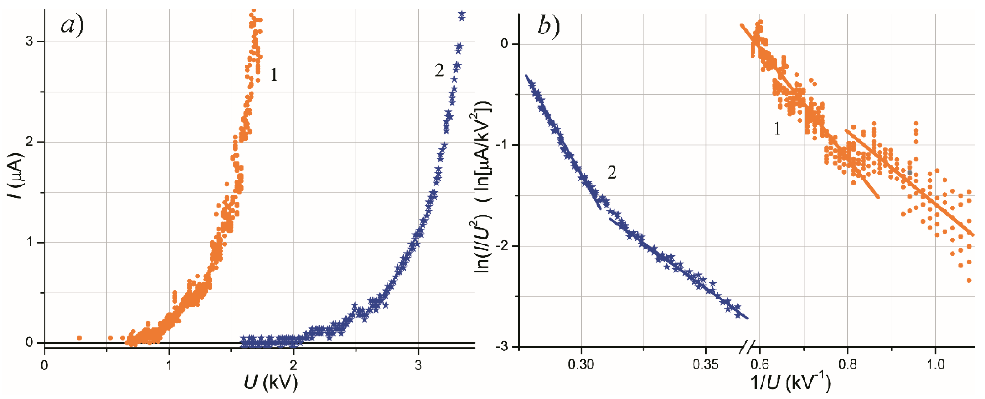
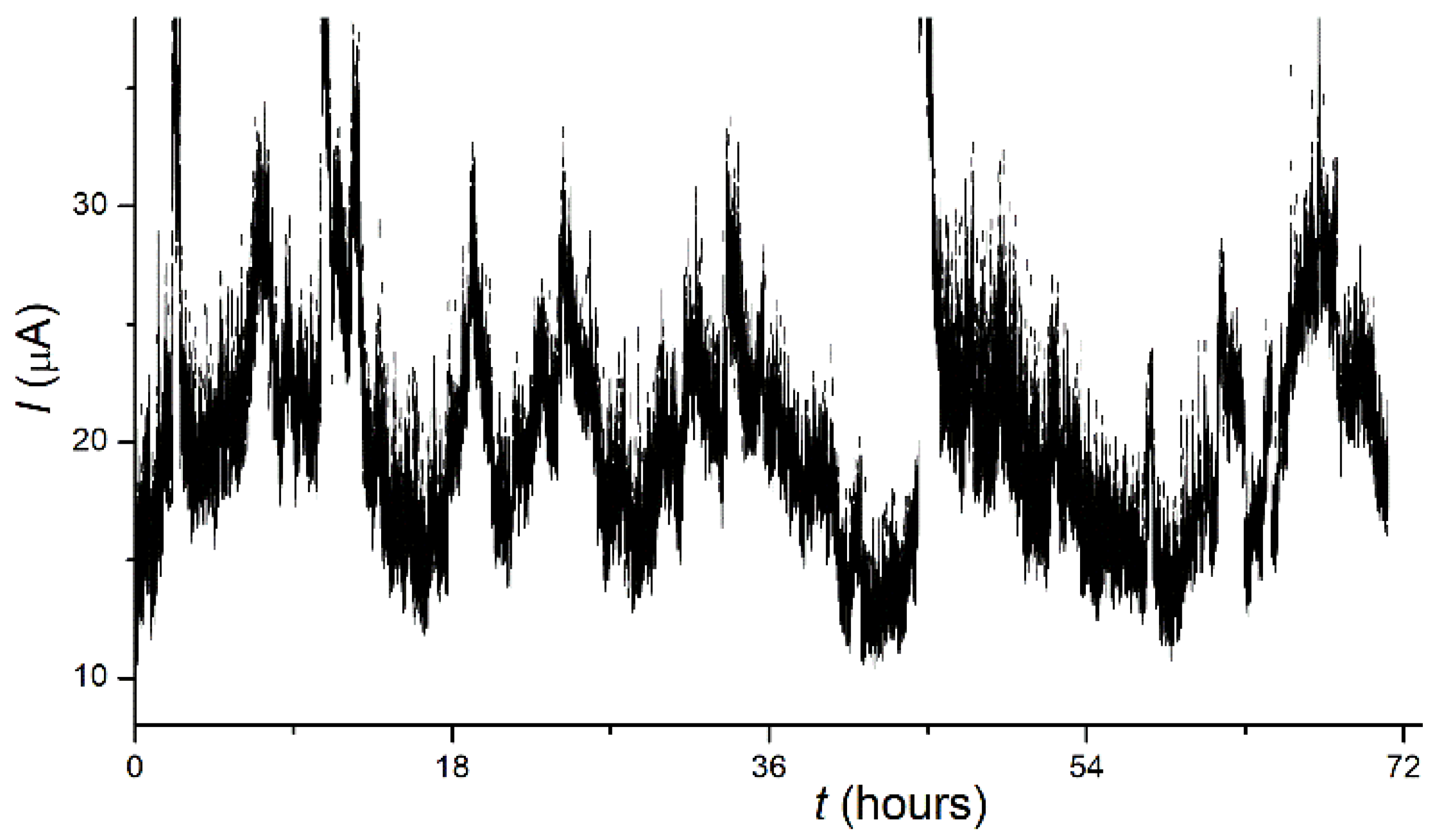
3.1. Emission Properties
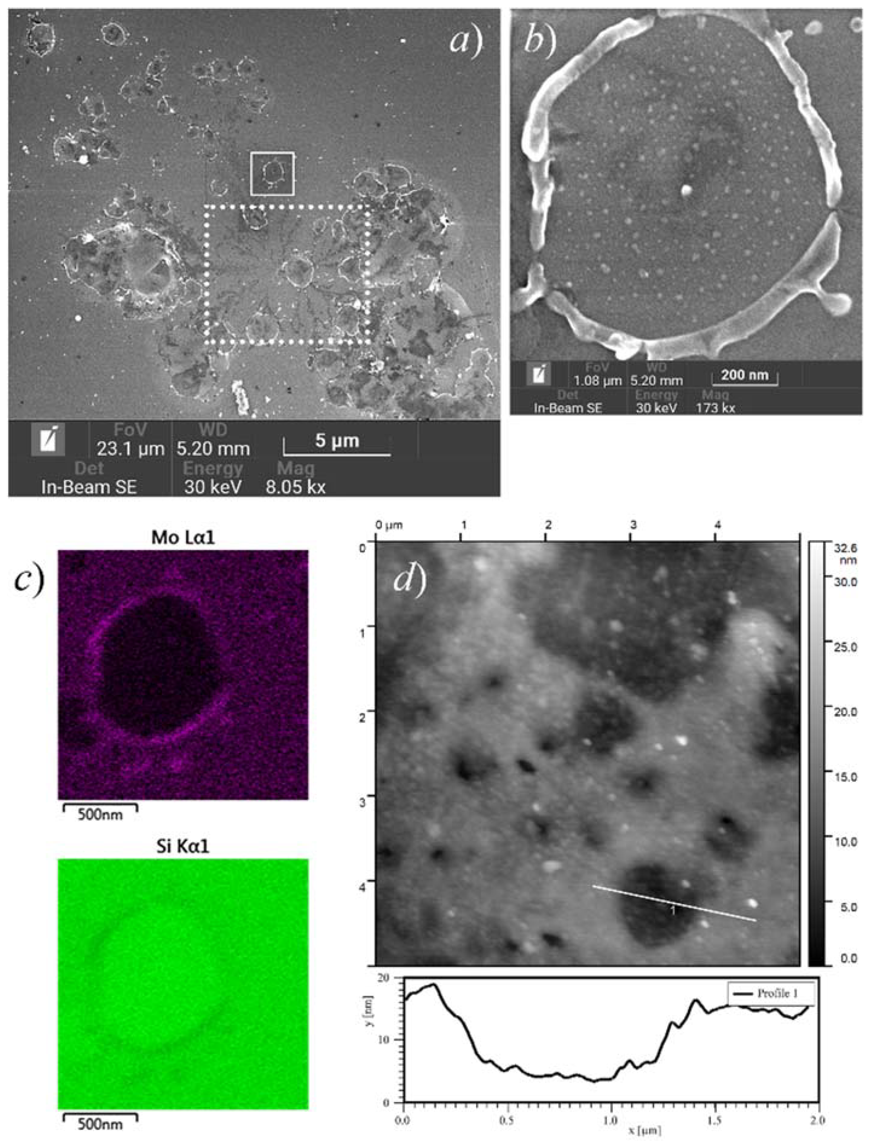
3.2. Surface Morphology
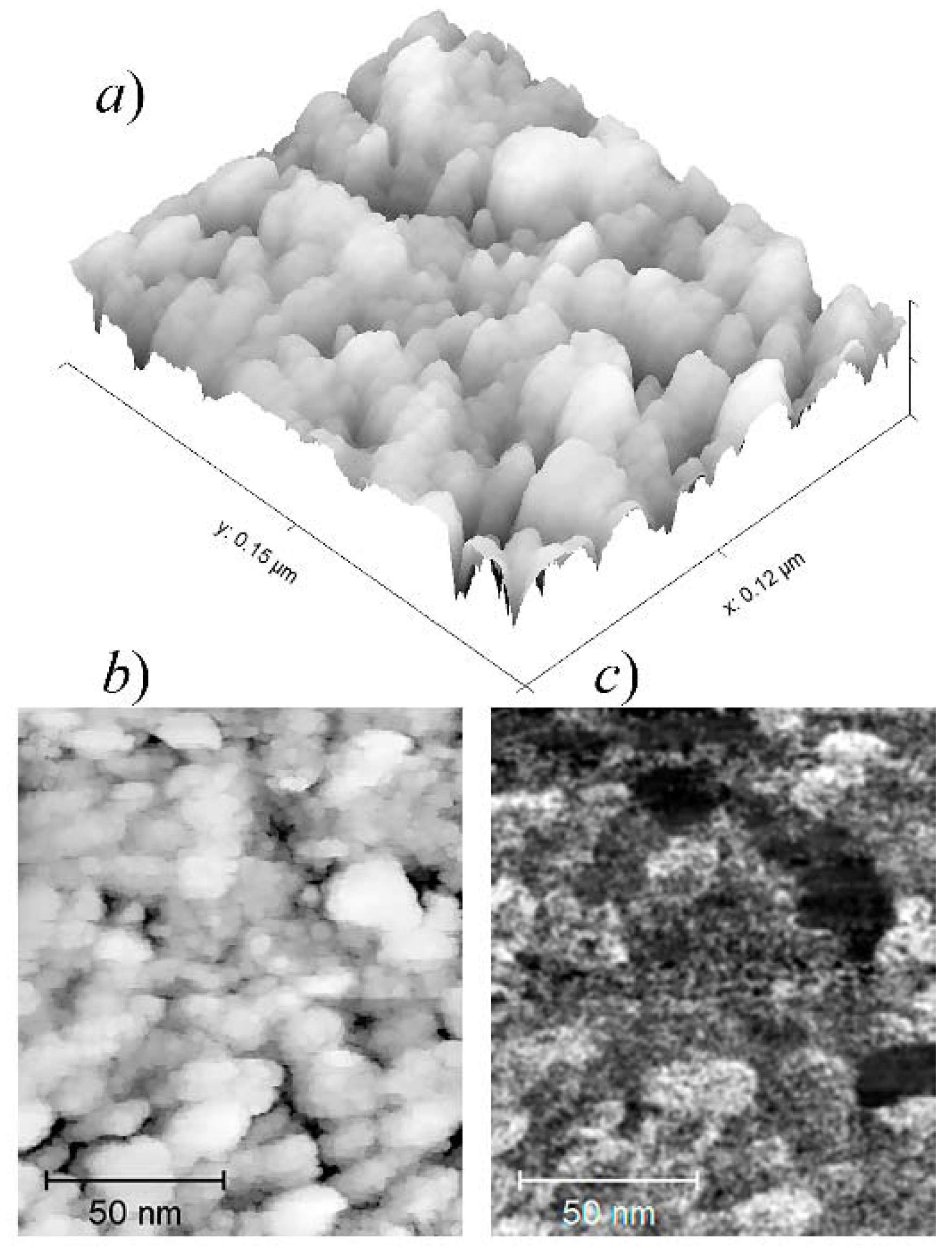
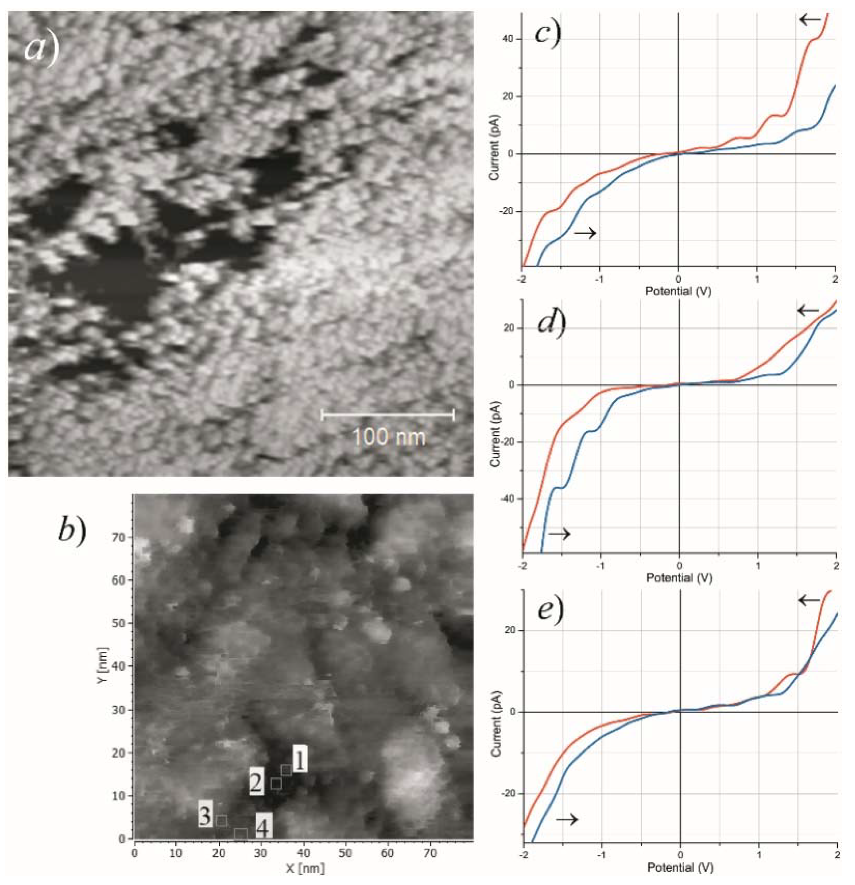
3.2.1. Pristine Films and Areas
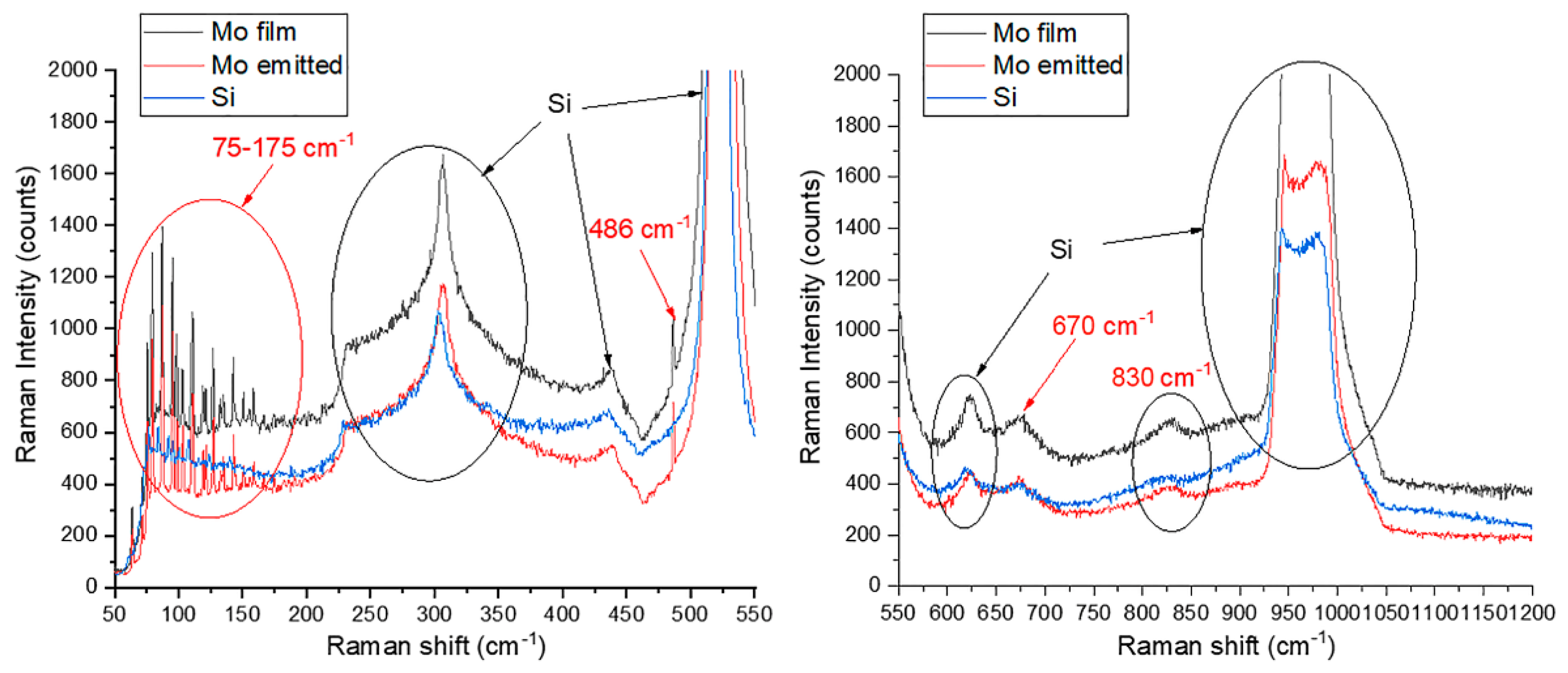
3.2.2. Raman Studies
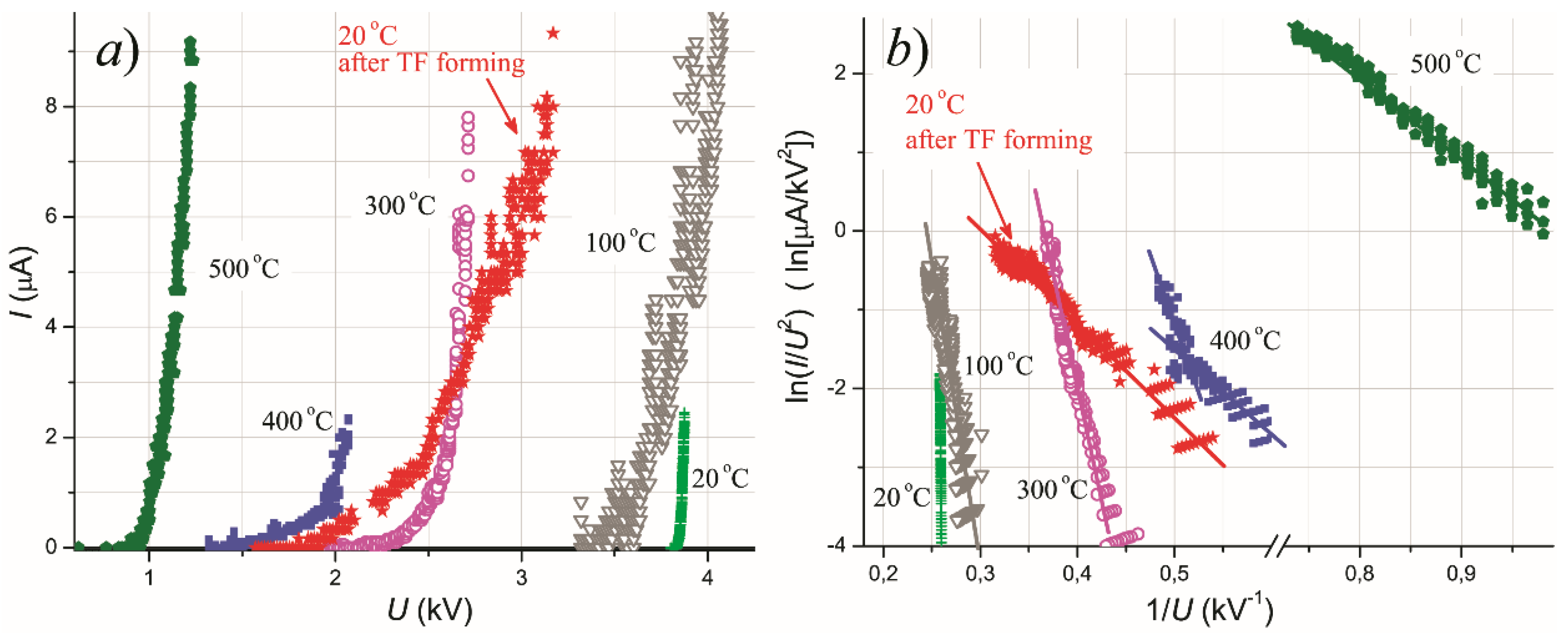
3.2.3. Effect of Forming
4. Discussion
4.1. Comparison with Literature Data
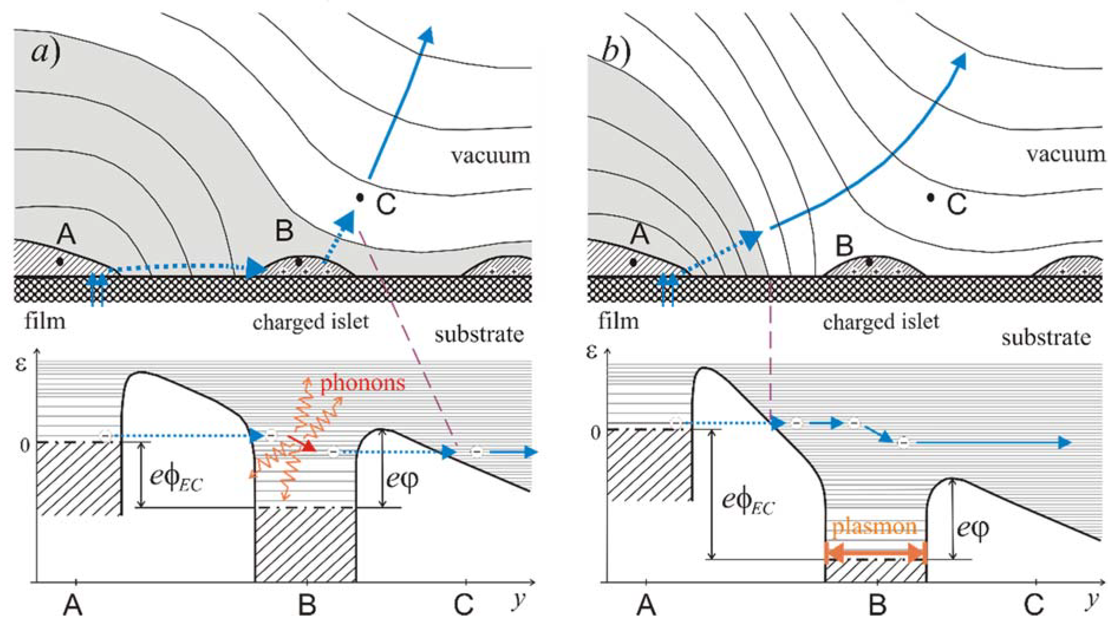
4.2. On the Emissiom Mechanism
4.3. Nanodot Emission Cell as Object for Further Studies
5. Conclusions
Author Contributions
Funding
Institutional Review Board Statement
Informed Consent Statement
Data Availability Statement
Acknowledgments
Conflicts of Interest
References
- Fursey, G.N. Field Emission in Vacuum Microelectronics; Kluwer Academic-Plenum Publishers: New York, NY, USA, 2005. [Google Scholar] [CrossRef]
- Evtukh, A.; Hartnagel, H.; Yilmazoglu, O.; Mimura, H.; Pavlidis, D. Vacuum Nanoelectronic Devices: Novel Electron Sources and Applications; John Wiley & Sons: Hoboken, NJ, USA, 2015. [Google Scholar] [CrossRef]
- Egorov, N.V.; Sheshin, E.P. Field Emission Electronics; Springer: Berlin/Heidelberg, Germany, 2017. [Google Scholar] [CrossRef]
- Bugaev, A.S.; Eroshkin, P.A.; Romanko, V.A.; Sheshin, E.P. Low-power X-ray tubes: The current status. Phys. Uspekhi 2013, 56, 691–703. [Google Scholar] [CrossRef]
- Basu, A.; Swanwick, M.E.; Fomani, A.A.; Velásquez-García, L.F. A portable x-ray source with a nanostructured Pt-coated silicon field emission cathode for absorption imaging of low-Z materials. J. Phys. D Appl. Phys. 2015, 48, 225501. [Google Scholar] [CrossRef] [Green Version]
- Giubileo, F.; Bartolomeo, A.; Iemmo, L.; Luongo, G.; Urban, F. Field Emission from carbon nanostructures. Appl. Sci. 2018, 8, 526. [Google Scholar] [CrossRef] [Green Version]
- Bugaev, A.S.; Kireev, V.B.; Sheshin, E.P.; Kolodyazhnyj, A.Y. Cathodoluminescent light sources: Status and prospects. Phys. Uspekhi 2015, 58, 792–818. [Google Scholar] [CrossRef]
- Yoo, S.T.; Ji, H.H.; Jung, S.K.; Kyu, C.P. Deep-ultraviolet light source with a carbon nanotube cold-cathode electron beam. J. Vac. Sci. Technol. B 2018, 36, 02C103. [Google Scholar] [CrossRef]
- Wu, C.S.; Makiuchi, Y.; Chen, C. High-energy electron beam lithography for nanoscale fabrication. In Lithography; Wang, M., Ed.; IntechOpen: London, UK, 2010; pp. 241–266. [Google Scholar] [CrossRef] [Green Version]
- Spindt, C.A. A thin-film field-emission cathode. J. Appl. Phys. 1968, 39, 3504–3505. [Google Scholar] [CrossRef]
- Egorov, N.V.; Sheshin, E.P. On the current state of field-emission electronics. J. Surf. Investig. 2017, 11, 285–294. [Google Scholar] [CrossRef]
- Milne, W.I.; Teo, K.B.K.; Amaratunga, G.A.J.; Legagneux, P.; Gangloff, L.; Schnell, J.-P.; Semet, V.; Thien Binh, V.; Groening, O. Carbon nanotubes as field emission sources. J. Mater. Chem. 2004, 14, 933–943. [Google Scholar] [CrossRef]
- Eletskii, A.V. Carbon nanotube-based electron field emitters. Phys. Uspekhi 2010, 53, 863–892. [Google Scholar] [CrossRef]
- Filip, V.; Filip, L.D.; Wong, H. Review on peculiar issues of field emission in vacuum nanoelectronic devices. Solid State Electron. 2017, 138, 3–15. [Google Scholar] [CrossRef]
- Mead, C.A. Operation of tunnel-emission devices. J. Appl. Phys. 1961, 32, 646–652. [Google Scholar] [CrossRef] [Green Version]
- Yokoo, K.; Tanaka, H.; Sato, S.; Murota, J.; Ono, S. Emission characteristics of metal–oxide–semiconductor electron tunneling cathode. J. Vac. Sci. Technol. 1993, 11, 429–432. [Google Scholar] [CrossRef]
- Adachi, H. Emission characteristics of metal–insulator–metal tunnel cathodes. J. Vac. Sci. Technol. 1996, 14, 2093–2095. [Google Scholar] [CrossRef]
- Yankelewitch, Y.B. The thin film metal-insulator-metal system used as a non-heated source of electrons. Vacuum 1980, 30, 97–107. [Google Scholar] [CrossRef]
- Thomsen, L.B.; Nielsen, G.; Vendelbo, S.B.; Johansson, M.; Hansen, O.; Chorkendorff, I. Electron emission from ultralarge area metal-oxide-semiconductor electron emitters. J. Vac. Sci. Technol. B 2009, 27, 562–567. [Google Scholar] [CrossRef]
- Fitting, H.-J.; Hingst, T.; Schreiber, E. Breakdown and high-energy electron vacuum emission of MIS-structures. J. Phys. D 1999, 32, 1963–1970. [Google Scholar] [CrossRef]
- Thurstans, R.E.; Oxley, D.P. The electroformed metal-insulator-metal structure: A comprehensive model. J. Phys. D 2002, 35, 802–809. [Google Scholar] [CrossRef]
- Kusunoki, T.; Suzuki, M.; Sagawa, M.; Mikami, Y.; Nishimura, E.; Ikeda, M.; Hirano, T.; Tsuji, K. Highly efficient and long life metal–insulator–metal cathodes. J. Vac. Sci. Technol. B 2012, 30, 041202. [Google Scholar] [CrossRef]
- Hu, Y.; Zhang, X.; Xue, T.; Liu, C. Characteristics of electron emission of Al-Al2O3-Ti/Au diode with a new double-layer insulator. J. Vac. Sci. Technol. B 2014, 32, 062204. [Google Scholar] [CrossRef]
- Wenger, C.; Kitzmann, J.; Wolff, A.; Fraschke, M.; Walczyk, C.; Lupina, G.; Mehr, W.; Junige, M.; Albert, M.; Bartha, J.W. Graphene based electron field emitter. J. Vac. Sci. Technol. B 2015, 33, 01A109. [Google Scholar] [CrossRef]
- Kirley, M.P.; Aloui, T.; Glass, J.T. Monolayer graphene-insulator-semiconductor emitter for large-area electron lithography. Appl. Phys. Lett. 2017, 110, 233109. [Google Scholar] [CrossRef]
- Murakami, K.; Adachi, M.; Miyaji, J.; Furuya, R.; Nagao, M.; Yamada, Y.; Neo, Y.; Takao, Y.; Sasaki, M.; Mimura, H. Mechanism of highly efficient electron emission from graphene/oxide/semiconductor structure. ACS Appl. Electron. Mater. 2020, 2, 2265–2273. [Google Scholar] [CrossRef]
- Nepijko, S.A.; Kutnyakhov, D.; Protsenko, S.I.; Odnodvorets, L.V.; Schönhense, G. Sensor and microelectronic elements based on nanoscale granular systems. J. Nanopart. Res. 2011, 13, 6263–6281. [Google Scholar] [CrossRef]
- Shen, Z.; Wang, X.; Wu, S.; Tian, J. Numerical analysis of the surface-conduction electron-emitter with a new configuration. Mod. Phys. Lett. B 2016, 30, 1650137. [Google Scholar] [CrossRef]
- Fedorovich, R.D.; Naumovets, A.D.; Tomchuk, P.M. Electronic phenomena in nanodispersed thin films. J. Phys. Condens. Matter 1999, 11, 9955–9967. [Google Scholar] [CrossRef]
- Fedorovich, R.D.; Naumovets, A.D.; Tomchuk, P.M. Electron and light emission from island metal films and generation of hot electrons in nanoparticles. Phys. Rep. 2000, 328, 73–179. [Google Scholar] [CrossRef]
- Bilotsky, Y.; Tomchuk, P.M. Peculiarity of electron–phonon energy exchange in metal nanoparticles and thin films. Surf. Sci. 2008, 602, 383–390. [Google Scholar] [CrossRef]
- Tomchuk, P.; Bilotsky, Y. New peculiarity in the temperature and size dependence of electron-lattice energy exchange in metal nanoparticle. Int. J. Mod. Phys. B 2014, 28, 145–220. [Google Scholar] [CrossRef] [Green Version]
- Fesenko, I.P.; Viduta, L.B.; Chasnyk, V.I.; Nechytailo, V.B.; Butenko, D.V.; Tkach, V.M.; Turkevich, V.Z.; Marchenko, O.A.; Zelenska, I.I.; Kaidash, O.M.; et al. Structure and current-voltage characteristics of islet gold films on high-heat conducting pressureless sintered AlN ceramics. J. Superhard Mater. 2018, 40, 432–434. [Google Scholar] [CrossRef]
- Gloskovskii, A.; Valdaitsev, D.A.; Cinchetti, M.; Nepijko, S.A.; Lange, J.; Aeschlimann, M.; Bauer, M.; Klimenkov, M.; Viduta, L.V.; Tomchuk, P.M.; et al. Electron emission from films of Ag and Au nanoparticles excited by a femtosecond pump-probe laser. Phys. Rev. B 2008, 77, 195427. [Google Scholar] [CrossRef] [Green Version]
- Ganichev, D.A.; Dokuchaev, V.S.; Fridrikhov, S.A.; Borziak, P.G.; Zavialov, Y.G.; Kulyupin, Y.A. Electron emission from discontinuous metal films in UHF Field. Pisma v Zhurnal Tekhnicheskoy Fiziki 1975, 62, 386–388. (In Russian) [Google Scholar]
- Araki, H.; Hanawa, T. Electron emission from electroformed carbon films. Vacuum 1998, 38, 31–35. [Google Scholar] [CrossRef]
- Bischoff, M.; Pagnia, H.; Trickl, J. Energy distribution of emitted electrons from electroformed MIM structures: The carbon island model. Int. J. Electron. 1992, 73, 1009–1010. [Google Scholar] [CrossRef]
- Arkhipov, A.V.; Gabdullin, P.G.; Gordeev, S.K.; Zhurkin, A.M.; Kvashenkina, O.E. Photostimulation of conductivity and electronic properties of field-emission nanocarbon coatings on silicon. Tech. Phys. 2017, 62, 127–136. [Google Scholar] [CrossRef]
- Andronov, A.; Budylina, E.; Shkitun, P.; Gabdullin, P.; Gnuchev, N.; Kvashenkina, O.; Arkhipov, A. Characterization of thin carbon films capable of low-field electron emission. J. Vac. Sci. Technol. B 2018, 36, 02C108. [Google Scholar] [CrossRef]
- Gabdullin, P.; Zhurkin, A.; Osipov, V.; Besedina, N.; Kvashenkina, O.; Arkhipov, A. Thin carbon films: Correlation between morphology and field-emission capability. Diam. Relat. Mater. 2020, 105, 107805. [Google Scholar] [CrossRef]
- Negishi, N.; Chuman, T.; Iwasaki, S.; Yoshikawa, T.; Ito, H.; Ogasawara, K. High efficiency electron-emission in Pt/SiOx/Si/Al structure. Jpn. J. Appl. Phys. 1997, 36, L939–L941. [Google Scholar] [CrossRef]
- Forbes, R.G. Low-macroscopic-field electron emission from carbon films and other electrically nanostructured heterogeneous materials: Hypotheses about emission mechanism. Solid State Electron. 2001, 45, 779–808. [Google Scholar] [CrossRef]
- Xu, N.S.; Huq, S.E. Novel cold cathode materials and applications. Mater. Sci. Eng. R Rep. 2005, 48, 47–189. [Google Scholar] [CrossRef]
- Eidelman, E.D.; Arkhipov, A.V. Field emission from carbon nanostructures: Models and experiment. Phys. Uspekhi 2020, 63, 648–667. [Google Scholar] [CrossRef]
- Robertson, J. Mechanisms of electron field emission from diamond, diamond-like carbon, and nanostructured carbon. J. Vac. Sci. Technol. B 1999, 17, 659–665. [Google Scholar] [CrossRef]
- Karabutov, A.V.; Frolov, V.D.; Konov, V.I.; Ralchenko, V.G.; Gordeev, S.K.; Belobrov, P.I. Low-field electron emission of diamond/pyrocarbon composites. J. Vac. Sci. Technol. B 2001, 19, 965–970. [Google Scholar] [CrossRef]
- Kleshch, V.I.; Vasilieva, E.A.; Lyashenko, S.A.; Obronov, I.V.; Turnina, A.V.; Obraztsov, A.N. Surface structure and field emission properties of few-layer graphene flakes. Phys. Status Solidi B 2011, 248, 2623–2626. [Google Scholar] [CrossRef]
- Arkhipov, A.; Davydov, S.; Gabdullin, P.; Gnuchev, N.; Kravchik, A.; Krel, S. Field-induced electron emission from nanoporous carbons. J. Nanomater. 2014, 2014, 190232. [Google Scholar] [CrossRef]
- Bandurin, D.A.; Mingels, S.; Kleshch, V.I.; Luetzenkirchen-Hecht, D.; Mueller, G.; Obraztsov, A.N. Field emission spectroscopy evidence for dual-barrier electron tunnelling in nanographite. Appl. Phys. Lett. 2015, 106, 233112. [Google Scholar] [CrossRef]
- Haque, A.; Narayan, J. Electron field emission from Q-carbon. Diam. Relat. Mater. 2018, 86, 71–78. [Google Scholar] [CrossRef]
- Fursey, G.N.; Polyakov, M.A.; Bagraev, N.T.; Zakirov, I.I.; Nashchekin, A.V.; Bocharov, V.N. Low-threshold field emission from carbon structures. J. Surf. Investig. 2019, 13, 814–824. [Google Scholar] [CrossRef]
- Davidovich, M.V.; Yafarov, R.K. Pulsed and static field emission VAC of carbon nanocluster structures: Experiment and its interpretation. Tech. Phys. 2019, 64, 1210–1220. [Google Scholar] [CrossRef]
- Karabutov, A.V.; Frolov, V.D.; Konov, V.I. Diamond-sp2 bonded carbon structures: Quantum well field electron emission? Diam. Relat. Mater. 2001, 10, 840–846. [Google Scholar] [CrossRef]
- Obraztsov, A.N.; Zakhidov, A.A. Low-field electron emission from nano-carbons. Diam. Relat. Mater. 2004, 13, 1044–1049. [Google Scholar] [CrossRef]
- Kokkorakis, G.C.; Xanthakis, J.P. Local electric field and enhancement factor around nanographitic structures embedded in amorphous carbon. Surf. Interface Anal. 2007, 39, 135–138. [Google Scholar] [CrossRef]
- Forbes, R.G.; Xanthakis, J.P. Field penetration into amorphous-carbon films: Consequences for field-induced electron emission. Surf. Interface Anal. 2007, 39, 139–145. [Google Scholar] [CrossRef]
- Yafyasov, A.; Bogevolnov, V.; Fursey, G.; Pavlov, G.; Polyakov, M.; Ibragimov, A. Low-threshold field emission from carbon nano-clusters. Ultramicroscopy 2011, 111, 409–414. [Google Scholar] [CrossRef]
- Fursei, G.M.; Polyakov, M.A.; Kantonistov, A.A.; Yafyasov, A.M.; Pavlov, B.S.; Bozhevol’nov, V.B. Field and explosive emissions from graphene-like structures. Tech. Phys. 2013, 58, 845–851. [Google Scholar] [CrossRef]
- Cui, J.B.; Ristein, J.; Ley, L. Low-threshold electron emission from diamond. Phys. Rev. B 1999, 60, 16135–16142. [Google Scholar] [CrossRef]
- Sominskii, G.G.; Sezonov, V.E.; Taradaev, S.P.; Vdovichev, S.N. Multilayer field emitters made of contacting hafnium and platinum nanolayers. Tech. Phys. 2019, 64, 116–120. [Google Scholar] [CrossRef]
- Lyashenko, D.A.; Svirko, Y.P.; Petrov, M.I.; Obraztsov, A.N. The laser assisted field electron emission from carbon nanostructure. J. Eur. Opt. Soc. Rapid 2017, 13, 4. [Google Scholar] [CrossRef] [Green Version]
- Arkhipov, A.V.; Eidelman, E.D.; Zhurkin, A.M.; Osipov, V.S.; Gabdullin, P.G. Low-field electron emission from carbon cluster films: Combined thermoelectric/hot-electron model of the phenomenon. Fuller. Nanotub. Carbon Nanostruct. 2020, 28, 286–294. [Google Scholar] [CrossRef]
- Bizyaev, I.S.; Gabdullin, P.G.; Gnuchev, N.M.; Arkhipov, A.V. Low-field emission of electrons by thin metal films: Effect of composition, deposition conditions and morphology on emission capability of a film. St. Petersburg State Polytech. Univ. J. Phys. Math. 2021, 14, 105–120. [Google Scholar] [CrossRef]
- Forbes, R.G. Comments on the continuing widespread and unnecessary use of a defective emission equation in field emission related literature. J. Appl. Phys. 2019, 126, 210901. [Google Scholar] [CrossRef] [Green Version]
- Forbes, R.G.; Deane, J.H.B. Reformulation of the standard theory of Fowler–Nordheim tunnelling and cold field electron emission. Proc. R. Soc. A Math. Phys. Eng. Sci. 2007, 463, 2907–2927. [Google Scholar] [CrossRef]
- Popov, E.O.; Kolosko, A.G.; Filippov, S.V. Test for compliance with the cold field emission regime using the Elinson–Schrednik and Forbes–Deane approximations (Murphy–Good plot). Tech. Phys. Lett. 2020, 46, 838–842. [Google Scholar] [CrossRef]
- Forbes, R.G.; Popov, E.O.; Kolosko, A.G.; Filippov, S.V. The pre-exponential voltage-exponent as a sensitive test parameter for field emission theories. R. Soc. Open Sci. 2021, 8, 201986. [Google Scholar] [CrossRef] [PubMed]
- Serbun, P.; Porshyn, V.; Müller, G.; Lützenkirchen-Hecht, D. Response to Comment on ‘Advanced field emission measurement techniques for research on modern cold cathode materials and their applications for transmission-type X-ray sources. Rev. Sci. Instrum. 2020, 91, 107102. [Google Scholar] [CrossRef]
- Bondarenko, V.B.; Gabdullin, P.G.; Gnuchev, N.M.; Davydov, S.N.; Korablev, V.V.; Kravchik, A.E.; Sokolov, V.V. Emissivity of powders prepared from nanoporous carbon. Tech. Phys. 2004, 49, 1360–1363. [Google Scholar] [CrossRef]
- Kruchinin, V.N.; Volodin, V.A.; Perevalov, T.V.; Gerasimova, A.K.; Aliev, V.S.; Gritsenko, V.A. Optical properties of nonstoichiometric tantalum oxide TaOx (x < 5/2) according to spectral-ellipsometry and Raman-scattering data. Opt. Spectrosc. 2018, 124, 808–813. [Google Scholar] [CrossRef]
- Py, M.A.; Schmid, P.E.; Vallin, J.T. Raman scattering and structural properties of MoO3. Il Nuovo Cim. B 1977, 38, 271–279. [Google Scholar] [CrossRef]
- Seguin, L.; Figlarz, M.; Cavagnat, R.; Lassègues, J.-C. Infrared and Raman spectra of MoO3 molybdenum trioxides and MoO3·xH2O molybdenum trioxide hydrates. Spectrochim. Acta Part A 1995, 51, 1323–1344. [Google Scholar] [CrossRef]
- Lunk, H.J.; Hartl, H.; Hartl, M.A.; Fait, M.J.G.; Shenderovich, I.G.; Feist, M.; Frisk, T.A.; Daemen, L.L.; Mauder, D.; Eckelt, R.; et al. Hexagonal molybdenum trioxide—Known for 100 years and still a fount of new discoveries. Inorg. Chem. 2010, 49, 9400–9408. [Google Scholar] [CrossRef]
- Filip, L.D.; Palumbo, M.; Carey, J.D.; Silva, S.R.P. Two-step electron tunneling from confined electronic states in a nanoparticle. Phys. Rev. B 2009, 79, 245429. [Google Scholar] [CrossRef] [Green Version]
- Raichev, O.E. Coulomb blockade of field emission from nanoscale conductors. Phys. Rev. B 2006, 73, 195328. [Google Scholar] [CrossRef] [Green Version]
- Kim, C.; Kim, H.S.; Qin, H.; Blick, R.H. Coulomb-controlled single electron field emission via a freely suspended metallic island. Nano Lett. 2010, 10, 615–619. [Google Scholar] [CrossRef]
- Kleshch, V.I.; Porshyn, V.; Lützenkirchen-Hecht, D.; Obraztsov, A.N. Coulomb blockade and quantum confinement in field electron emission from heterostructured nanotips. Phys. Rev. B 2020, 102, 235437. [Google Scholar] [CrossRef]
- Kleshch, V.I.; Porshyn, V.; Orekhov, A.S.; Lützenkirchen-Hecht, D.; Obraztsov, A.N. Carbon single-electron point source controlled by Coulomb blockade. Carbon 2021, 171, 154–160. [Google Scholar] [CrossRef]
- Kleshch, V.I.; Porshyn, V.; Serbun, P.; Orekhov, A.S.; Ismagilov, R.R.; Malykhin, S.A.; Eremina, V.A.; Obraztsova, E.D.; Obraztsov, A.N.; Lützenkirchen-Hecht, D. Coulomb blockade in field electron emission from carbon nanotubes. Appl. Phys. Lett. 2021, 118, 053101. [Google Scholar] [CrossRef]
- Thompson, C.V. Solid-state dewetting of thin films. Annu. Rev. Mater. Res. 2012, 42, 399–434. [Google Scholar] [CrossRef]
- Altomare, M.; Nguyen, N.T.; Schmuki, P. Templated dewetting: Designing entirely selforganized platforms for photocatalysis. Chem. Sci. 2016, 7, 6865. [Google Scholar] [CrossRef] [PubMed] [Green Version]
- Kovalenko, O.; Szabó, S.; Klinger, L.; Rabkin, E. Solid state dewetting of polycrystalline Mo film on sapphire. Acta Mater. 2017, 139, 51–61. [Google Scholar] [CrossRef]
- Kojima, Y.; Kato, T. Nanoparticle formation in Au thin films by electron-beam-induced dewetting. Nanotechnology 2008, 19, 255605. [Google Scholar] [CrossRef] [PubMed]
- Ruffino, F.; Grimaldi, G. Controlled dewetting as fabrication and patterning strategy for metal nanostructures. Phys. Status Solidi A 2015, 212, 1662–1684. [Google Scholar] [CrossRef]
- Tuzhilkin, M.S.; Bespalova, P.G.; Mishin, M.V.; Kolesnikov, I.E.; Karabeshkin, K.V.; Karaseov, P.A.; Titov, A.I. Formation of Au nanoparticles and features of etching of a Si substrate under irradiation with atomic and molecular ions. Semiconductors 2020, 54, 137–143. [Google Scholar] [CrossRef]
- Purohit, V.S.; Hise, A.B.; Dey, S.; More, M.A.; Dharmadhikari, C.V.; Joag, D.S.; Pasricha, R.; Bhoraskar, S.V. Scanning tunneling microscopic and field emission microscopic studies of nanostructured molybdenum film synthesized by electron cyclotron resonance plasma. Vacuum 2009, 83, 435–443. [Google Scholar] [CrossRef]
- Purohit, V.; Mazumder, B.; Bhise, A.B.; Poddar, P.; Joag, D.S.; Bhoraskar, S.V. Field emission studies of silver nanoparticles synthesized by electron cyclotron resonance plasma. Appl. Surf. Sci. 2011, 257, 7184–7189. [Google Scholar] [CrossRef]
- Arkhipov, A.V.; Gabdullin, P.G.; Mishin, M.V.; Protopopova, V.S.; Krel, S.I.; Drobinin, D.E.; Gnuchev, N.M. Field-emission properties of Ni-C nanocomposite films. J. Nano Electron. Phys. 2016, 8, 02058. [Google Scholar] [CrossRef]
- Modinos, A. Theoretical analysis of field emission data. Solid State Electron. 2001, 45, 809–816. [Google Scholar] [CrossRef]
- Chuvilin, A.L.; Kuznetsov, V.L.; Obraztsov, A.N. Chiral carbon nanoscrolls with a polygonal cross-section. Carbon 2009, 47, 3099–3105. [Google Scholar] [CrossRef]
- Kleshch, V.I.; Bandurin, D.A.; Serbun, P.; Ismagilov, R.R.; Lützenkirchen-Hecht, D.; Müller, G.; Obraztsov, A.N. Field electron emission from CVD nanocarbon films containing scrolled graphene structures. Phys. Status Solidi B 2018, 255, 1700270. [Google Scholar] [CrossRef]
- Koh, Y.K.; Lyons, A.S.; Bae, M.-H.; Huang, B.; Dorgan, V.E.; Cahill, D.G.; Pop, E. Role of remote interfacial phonon (RIP) scattering in heat transport across graphene/SiO2 interfaces. Nano Lett. 2016, 16, 6014–6020. [Google Scholar] [CrossRef] [Green Version]
- Ju, Y.S.; Goodson, K.E. Phonon scattering in silicon films with thickness of order 100 nm. Appl. Phys. Lett. 1999, 74, 3005–3007. [Google Scholar] [CrossRef]
- Chen, T.-G.; Yu, P.; Chou, R.-H.; Pan, C.-L. Phonon thermal conductivity suppression of bulk silicon nanowire composites for efficient thermoelectric conversion. Opt. Express 2010, 18, 467–476. [Google Scholar] [CrossRef] [PubMed] [Green Version]
- Eydelman, E.D.; Vul’, A.Y. The strong thermoelectric effect in nanocarbon generated by ballistic phonon drag of electrons. J. Phys. Condens. Matter 2007, 19, 266210–266223. [Google Scholar] [CrossRef]
- Eidelman, E.D. Thermoelectric mechanism of field emission from carbon nanostructures. Tech. Phys. 2019, 64, 1409–1417. [Google Scholar] [CrossRef]
- Inoshita, T.; Sakaki, H. Electron-phonon interaction and the so-called phonon bottleneck effect in semiconductor quantum dots. Phys. B Condens. Matter. 1996, 227, 373–377. [Google Scholar] [CrossRef]
- Nozik, A.J. Spectroscopy and hot electron relaxation dynamics in semiconductor quantum wells and quantum dots. Annu. Rev. Phys. Chem. 2001, 52, 193–231. [Google Scholar] [CrossRef] [PubMed]
- Pandey, A.; Guyot-Sionnest, P. Slow electron cooling in colloidal quantum dots. Science 2008, 322, 929–932. [Google Scholar] [CrossRef]
- Arbouet, A.; Voisin, C.; Christofilos, D.; Langot, P.; Del Fatti, N.; Vallée, F.; Lermé, J.; Celep, G.; Cottancin, E.; Gaudry, M.; et al. Electron-phonon scattering in metal clusters. Phys. Rev. Lett. 2003, 90, 177401. [Google Scholar] [CrossRef] [PubMed] [Green Version]
- Mongin, D.; Maioli, P.; Burgin, J.; Langot, P.; Cottancin, E.; D’Addato, S.; Canut, B.; Treguer, M.; Crut, A.; Vallée, F.; et al. Ultrafast electron-lattice thermalization in copper and other noble metal nanoparticles. J. Phys. Condens. Matter 2019, 31, 084001. [Google Scholar] [CrossRef] [PubMed] [Green Version]
- Zhu, S.; Song, Y.; Zhao, X.; Shao, J.; Zhang, J.; Yang, B. The photoluminescence mechanism in carbon dots (graphene quantum dots, carbon nanodots, and polymer dots): Current state and future perspective. Nano Res. 2015, 8, 355–381. [Google Scholar] [CrossRef]
- Fatimy, A.E.; Myers-Ward, R.L.; Boyd, A.K.; Daniels, K.M.; Gaskill, D.K.; Barbara, P. Epitaxial graphene quantum dots for high-performance terahertz bolometers. Nat. Nanotech. 2016, 11, 335–338. [Google Scholar] [CrossRef] [Green Version]
- Jiang, J.; Saito, R.; Greuneis, A.; Dresselhaus, G.; Dresselhaus, M.S. Electron–phonon interaction and relaxation time in graphite. Chem. Phys. Lett. 2004, 392, 383–389. [Google Scholar] [CrossRef]
- Dubois, S.M.-M.; Zanolli, Z.; Declerck, X.; Charlier, J.-C. Electronic properties and quantum transport in graphene-based nanostructures. Eur. Phys. J. 2009, 72, 1–24. [Google Scholar] [CrossRef]
- Liu, J.G.; Zhang, H.; Link, S.; Nordlander, P. Relaxation of plasmon-induced hot carriers. ACS Photonics 2018, 5, 2584–2595. [Google Scholar] [CrossRef]
- Borziak, P.G.; Kulyupin, Y.A. Investigations of discontinuous metal films in the U.S.S.R. Thin Solid Film. 1977, 44, 1–19. [Google Scholar] [CrossRef]
- Kalathingal, V.; Dawson, P.; Mitra, J. Scanning tunnelling microscope light emission: Finite temperature current noise and over cut-off emission. Sci. Rep. 2017, 7, 3530. [Google Scholar] [CrossRef] [PubMed] [Green Version]
- Willets, K.A.; van Duyne, R.P. Localized surface plasmon resonance spectroscopy and sensing. Annu. Rev. Phys. Chem. 2007, 58, 267–297. [Google Scholar] [CrossRef] [Green Version]
- Maity, S.; Bain, D.; Bhattacharyya, K.; Das, S.; Bera, R.; Jana, B.; Paramanik, B.; Datta, A.; Patra, A. Ultrafast relaxation dynamics of luminescent copper nanoclusters (Cu7L3) and efficient electron transfer to functionalized reduced graphene oxide. J. Phys. Chem. C 2018, 122, 13354–13362. [Google Scholar] [CrossRef]
- Gröning, O.; Nilsson, L.-O.; Gröning, P.; Schlapbach, L. Properties and characterization of chemical vapor deposition diamond field emitters. Solid State Electron. 2001, 45, 929–944. [Google Scholar] [CrossRef]
- Gu, Z.-G.; Li, D.-J.; Zheng, C.; Kang, Y.; Wöll, C.; Zhang, J. MOF-templated synthesis of ultrasmall photoluminescent carbon-nanodot arrays for optical applications. Angew. Chem. Int. Ed. 2017, 56, 6853–6858. [Google Scholar] [CrossRef] [PubMed]
- Gu, Z.-G.; Zhang, J. Epitaxial growth and applications of oriented metal–organic framework thin films. Coord. Chem. Rev. 2019, 378, 513–532. [Google Scholar] [CrossRef]


Publisher’s Note: MDPI stays neutral with regard to jurisdictional claims in published maps and institutional affiliations. |
© 2021 by the authors. Licensee MDPI, Basel, Switzerland. This article is an open access article distributed under the terms and conditions of the Creative Commons Attribution (CC BY) license (https://creativecommons.org/licenses/by/4.0/).
Share and Cite
Bizyaev, I.; Gabdullin, P.; Chumak, M.; Babyuk, V.; Davydov, S.; Osipov, V.; Kuznetsov, A.; Kvashenkina, O.; Arkhipov, A. Low-Field Electron Emission Capability of Thin Films on Flat Silicon Substrates: Experiments with Mo and General Model for Refractory Metals and Carbon. Nanomaterials 2021, 11, 3350. https://doi.org/10.3390/nano11123350
Bizyaev I, Gabdullin P, Chumak M, Babyuk V, Davydov S, Osipov V, Kuznetsov A, Kvashenkina O, Arkhipov A. Low-Field Electron Emission Capability of Thin Films on Flat Silicon Substrates: Experiments with Mo and General Model for Refractory Metals and Carbon. Nanomaterials. 2021; 11(12):3350. https://doi.org/10.3390/nano11123350
Chicago/Turabian StyleBizyaev, Ivan, Pavel Gabdullin, Maxim Chumak, Vladislav Babyuk, Sergey Davydov, Vasilii Osipov, Alexey Kuznetsov, Olga Kvashenkina, and Alexander Arkhipov. 2021. "Low-Field Electron Emission Capability of Thin Films on Flat Silicon Substrates: Experiments with Mo and General Model for Refractory Metals and Carbon" Nanomaterials 11, no. 12: 3350. https://doi.org/10.3390/nano11123350
APA StyleBizyaev, I., Gabdullin, P., Chumak, M., Babyuk, V., Davydov, S., Osipov, V., Kuznetsov, A., Kvashenkina, O., & Arkhipov, A. (2021). Low-Field Electron Emission Capability of Thin Films on Flat Silicon Substrates: Experiments with Mo and General Model for Refractory Metals and Carbon. Nanomaterials, 11(12), 3350. https://doi.org/10.3390/nano11123350