
Effect of Point Defects on Electronic Structure of Monolayer GeS


Abstract
:1. Introduction
2. Calculation Method
3. Results and Discussion
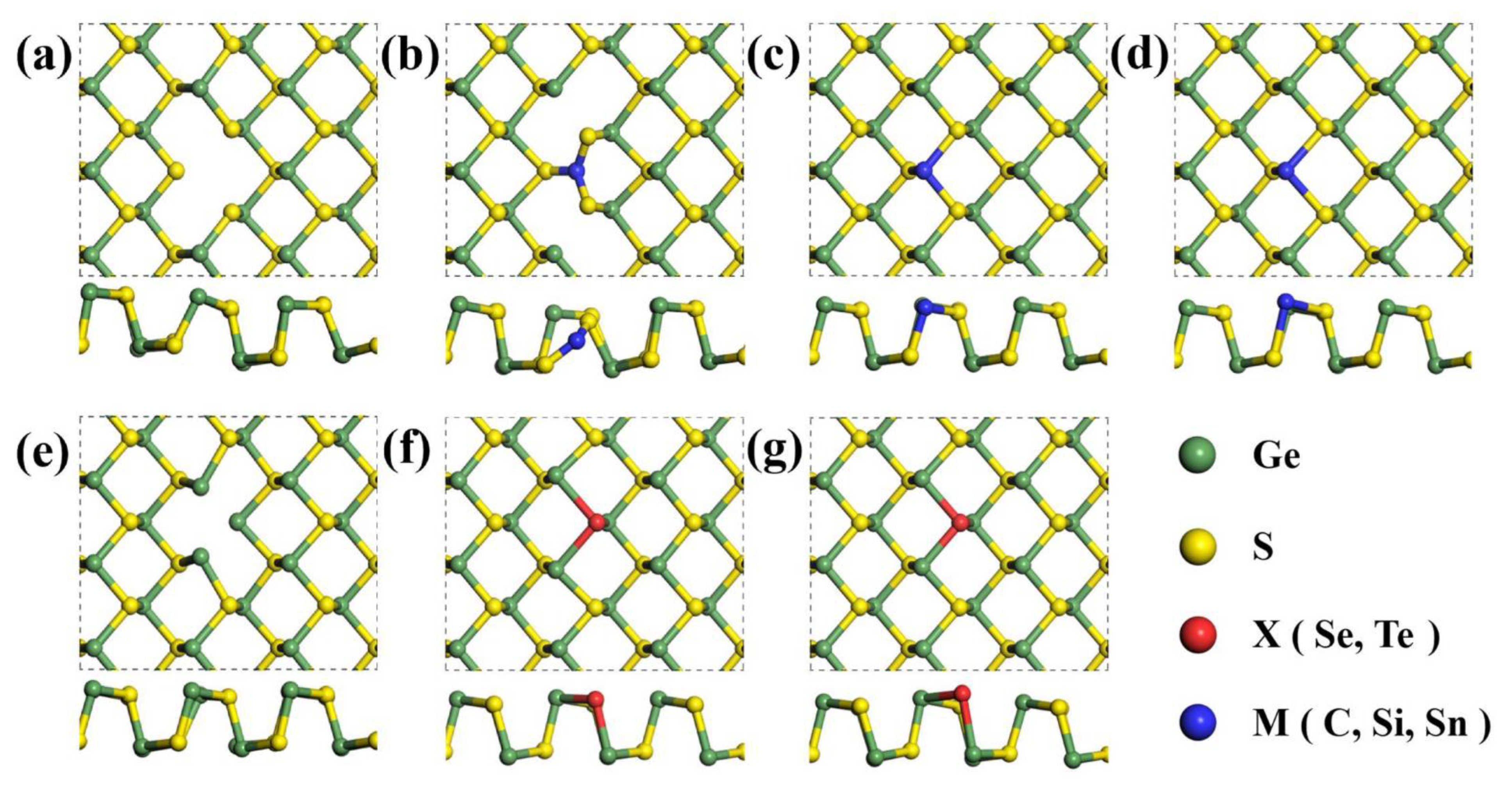
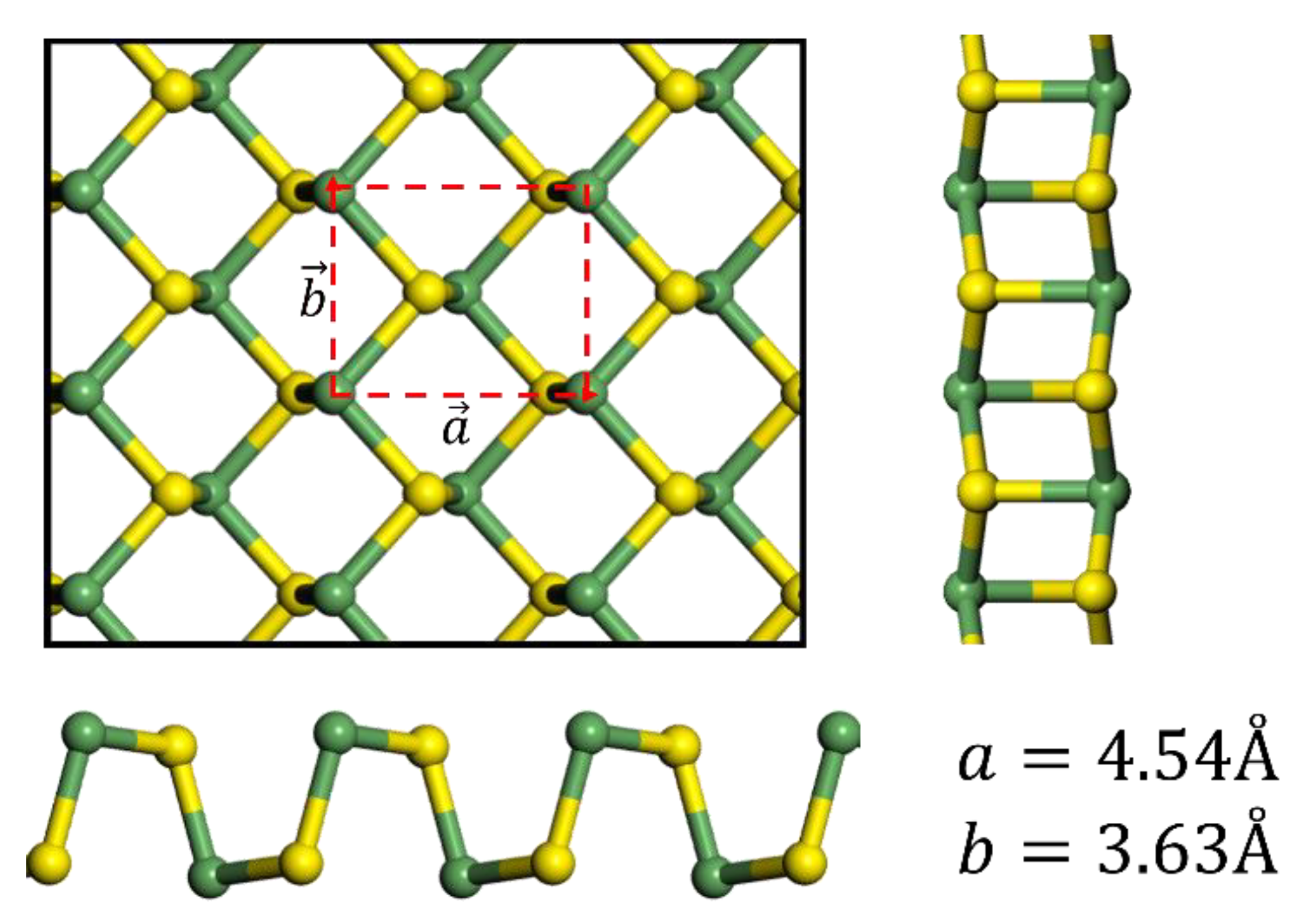
3.1. Crystal Structure and Energetics
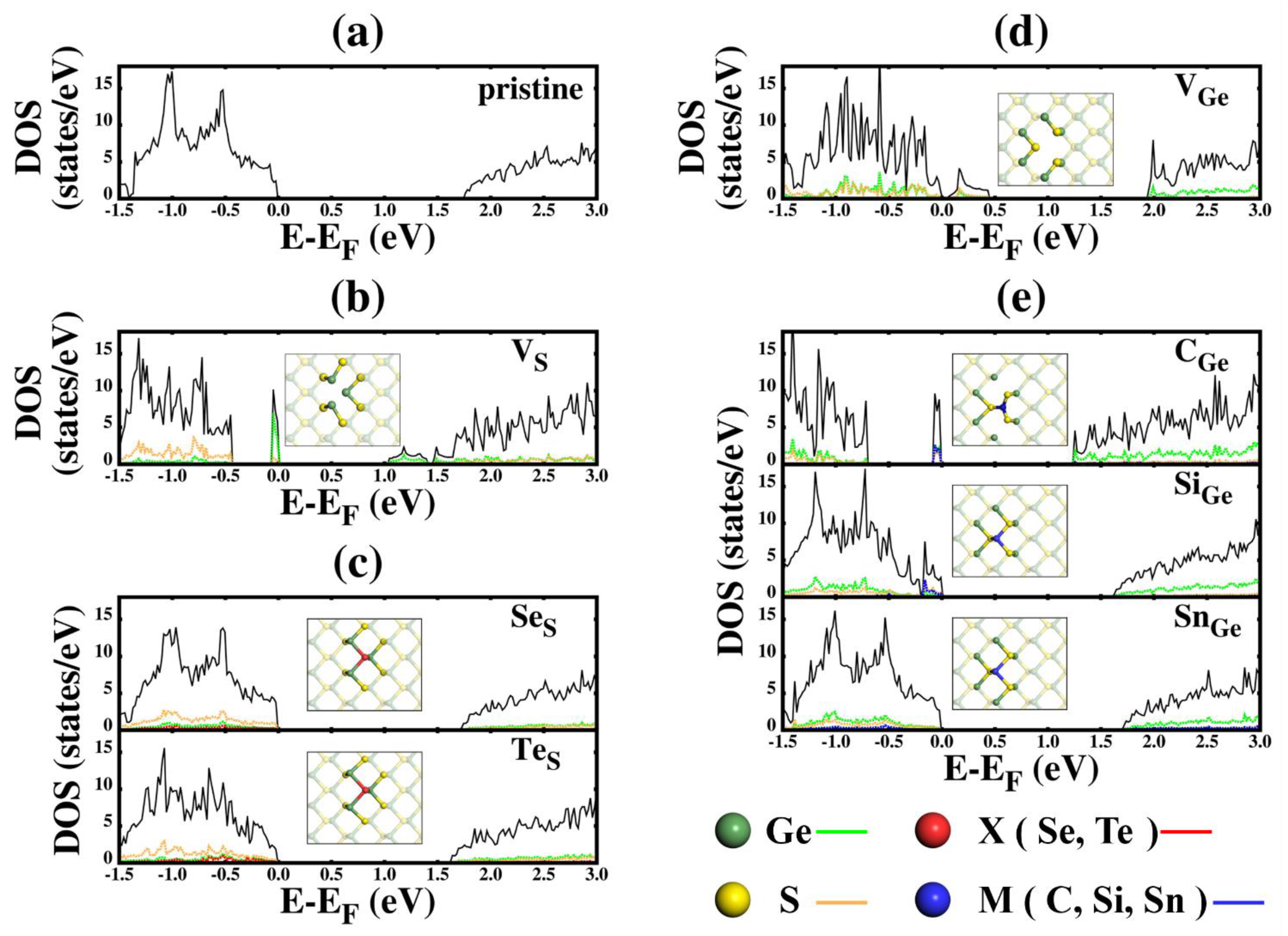
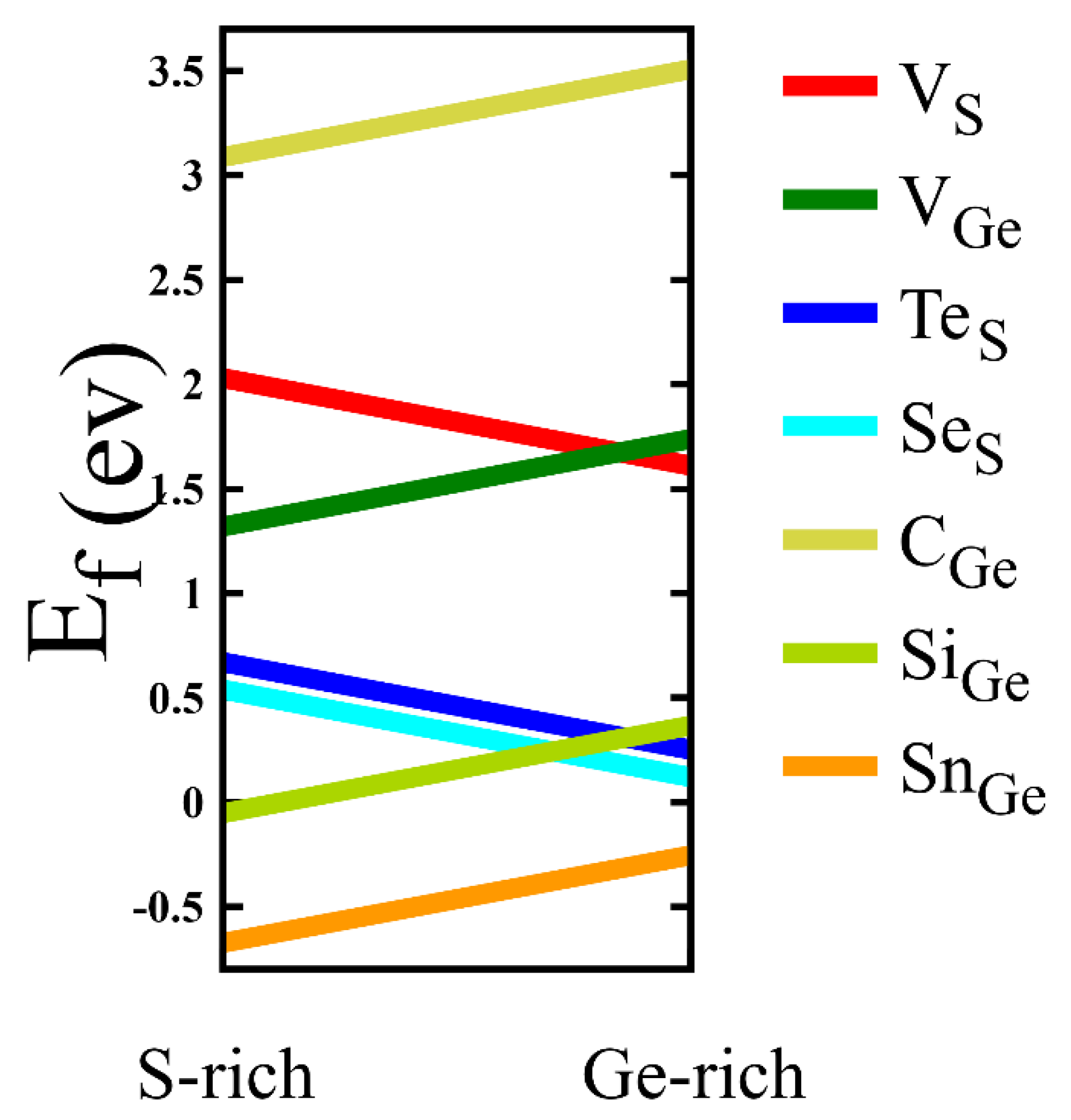
3.2. Electronic Properties
3.3. Piezoelectric Properties
4. Conclusions
Supplementary Materials
Author Contributions
Funding
Conflicts of Interest
References
- Wallace, P.R. The Band Theory of Graphite. Phys. Rev. 1947, 71, 622. [Google Scholar] [CrossRef]
- Novoselov, K.S.; Geim, A.K.; Morozov, S.V.; Jiang, D.; Zhang, Y.; Dubonos, S.V.; Grigorieva, I.V.; Firsov, A.A. Electric Field Effect in Atomically Thin Carbon Films. Science 2004, 306, 666. [Google Scholar] [CrossRef] [Green Version]
- Neto, A.H.C.; Guinea, F.; Peres, N.M.R.; Novoselov, K.S.; Geim, A.K. The electronic properties of graphene. Rev. Mod. Phys. 2009, 81, 109–162. [Google Scholar] [CrossRef] [Green Version]
- Banszerus, L.; Schmitz, M.; Engels, S.; Dauber, J.; Oellers, M.; Haupt, F.; Watanabe, K.; Taniguchi, T.; Beschoten, B.; Stampfer, C. Ultrahigh-mobility graphene devices from chemical vapor deposition on reusable copper. Sci. Adv. 2015, 1, e1500222. [Google Scholar] [CrossRef] [Green Version]
- Pop, E.; Varshney, V.; Roy, A.K. Thermal properties of graphene: Fundamentals and applications. MRS Bull. 2012, 37, 1273–1281. [Google Scholar] [CrossRef] [Green Version]
- Chhowalla, M.; Shin, H.S.; Eda, G.; Li, L.-J.; Loh, K.; Zhang, H. The chemistry of two-dimensional layered transition metal dichalcogenide nanosheets. Nat. Chem. 2013, 5, 263–275. [Google Scholar] [CrossRef] [PubMed]
- Wang, Q.H.; Kalantar-Zadeh, K.; Kis, A.; Coleman, J.; Strano, M.S. Electronics and optoelectronics of two-dimensional transition metal dichalcogenides. Nat. Nanotechnol. 2012, 7, 699–712. [Google Scholar] [CrossRef]
- Lv, R.; Robinson, J.A.; Schaak, R.E.; Sun, D.; Sun, Y.; Mallouk, T.E.; Terrones, M. Transition Metal Dichalcogenides and Beyond: Synthesis, Properties, and Applications of Single- and Few-Layer Nanosheets. Accounts Chem. Res. 2015, 48, 56–64. [Google Scholar] [CrossRef] [PubMed]
- Mak, K.F.; Shan, K.F.M.J. Photonics and optoelectronics of 2D semiconductor transition metal dichalcogenides. Nat. Photonics 2016, 10, 216–226. [Google Scholar] [CrossRef]
- Cha, J.; Min, K.-A.; Sung, D.; Hong, S. Ab initio study of adsorption behaviors of molecular adsorbates on the surface and at the edge of MoS 2. Curr. Appl. Phys. 2018, 18, 1013–1019. [Google Scholar] [CrossRef]
- Kim, J.; Choi, C.-G.; Min, K.-A.; Cho, K.; Hong, S. Effect of atomic passivation at Ni-MoS2 interfaces on contact behaviors. Curr. Appl. Phys. 2020, 20, 132–136. [Google Scholar] [CrossRef]
- Min, K.-A.; Park, J.; Wallace, R.; Cho, K.; Hong, S. Reduction of Fermi level pinning at Au–MoS 2 interfaces by atomic passivation on Au surface. 2D Mater. 2016, 4, 015019. [Google Scholar] [CrossRef]
- Zhang, Z.Y.; Si, M.S.; Wang, Y.H.; Gao, X.P.; Sung, D.; Hong, S.; He, J. Indirect-direct band gap transition through electric tuning in bilayer MoS2. J. Chem. Phys. 2014, 140, 174707. [Google Scholar] [CrossRef] [PubMed]
- Santosh, K.C.; Zhang, C.; Hong, S.; Wallace, R.M.; Cho, K. Phase stability of transition metal dichalcogenide by competing ligand field stabilization and charge density wave. 2D Mater. 2015, 2, 035019. [Google Scholar] [CrossRef]
- Zhang, C.; Gong, C.; Nie, Y.; Min, K.-A.; Liang, C.; Oh, Y.J.; Zhang, H.; Wang, W.; Hong, S.; Colombo, L.; et al. Systematic study of electronic structure and band alignment of monolayer transition metal dichalcogenides in Van der Waals heterostructures. 2D Mater. 2016, 4, 015026. [Google Scholar] [CrossRef]
- Zhang, C.; Kc, S.; Nie, Y.; Liang, C.; Vandenberghe, W.G.; Longo, R.C.; Zheng, Y.; Kong, F.; Hong, S.; Wallace, R.M.; et al. Charge Mediated Reversible Metal–Insulator Transition in Monolayer MoTe2 and WxMo1–xTe2 Alloy. ACS Nano 2016, 10, 7370–7375. [Google Scholar] [CrossRef]
- Fei, R.; Yang, L. Strain-Engineering the Anisotropic Electrical Conductance of Few-Layer Black Phosphorus. Nano Lett. 2014, 14, 2884–2889. [Google Scholar] [CrossRef] [Green Version]
- Qiao, J.; Kong, X.; Hu, Z.-X.; Yang, F.; Ji, W. High-mobility transport anisotropy and linear dichroism in few-layer black phosphorus. Nat. Commun. 2014, 5, 4475. [Google Scholar] [CrossRef] [Green Version]
- Li, L.; Yu, Y.; Ye, G.J.; Ge, Q.; Ou, X.; Wu, H.; Feng, D.; Chen, X.H.; Zhang, Y. Black phosphorus field-effect transistors. Nat. Nanotechnol. 2014, 9, 372–377. [Google Scholar] [CrossRef] [Green Version]
- Liu, Q.; Zhang, X.; Abdalla, L.B.; Fazzio, A.; Zunger, A. Switching a Normal Insulator into a Topological Insulator via Electric Field with Application to Phosphorene. Nano Lett. 2015, 15, 1222–1228. [Google Scholar] [CrossRef] [Green Version]
- Gomes, L.C.; Carvalho, A.; Neto, A.H.C. Vacancies and oxidation of two-dimensional group-IV monochalcogenides. Phys. Rev. B 2016, 94, 054103. [Google Scholar] [CrossRef] [Green Version]
- Haq, B.U.; AlFaify, S.; Ahmed, R.; Butt, F.K.; Laref, A.; Shkir, M. Exploring single-layered SnSe honeycomb polymorphs for optoelectronic and photovoltaic applications. Phys. Rev. B 2018, 97, 075438. [Google Scholar] [CrossRef]
- Xia, C.; Du, J.; Xiong, W.; Jia, Y.; Wei, Z.; Li, J. A type-II GeSe/SnS heterobilayer with a suitable direct gap, superior optical absorption and broad spectrum for photovoltaic applications. J. Mater. Chem. A 2017, 5, 13400–13410. [Google Scholar] [CrossRef]
- Hu, Z.-Y.; Li, K.-Y.; Lu, Y.; Huang, Y.; Shao, X.-H. High thermoelectric performances of monolayer SnSe allotropes. Nanoscale 2017, 9, 16093–16100. [Google Scholar] [CrossRef]
- Zhao, L.-D.; Lo, S.-H.; Zhang, Y.S.; Sun, H.; Tan, G.H.; Uher, C.; Wolverton, C.M.; Dravid, V.P.; Kanatzidis, M.G. Ultralow thermal conductivity and high thermoelectric figure of merit in SnSe crystals. Nat. Cell Biol. 2014, 508, 373–377. [Google Scholar] [CrossRef]
- Zhao, L.D.; Tan, G.; Hao, S.; He, J.; Pei, Y.; Chi, H.; Wang, H.; Gong, S.; Xu, H.; Dravid, V.P.; et al. Ultrahigh power factor and thermoelectric performance in hole-doped single-crystal SnSe. Science 2016, 351, 141–144. [Google Scholar] [CrossRef] [Green Version]
- Shi, G.; Kioupakis, E. Quasiparticle band structures and thermoelectric transport properties of p-type SnSe. J. Appl. Phys. 2015, 117, 065103. [Google Scholar] [CrossRef] [Green Version]
- Solanki, G.K.; Deshpande, M.P.; Agarwal, M.K.; Patel, P.D.; Vaidya, S.N. Thermoelectric power factor measurements in GeSe single crystals grown using different transporting agents. J. Mater. Sci. Lett. 2003, 22, 985–987. [Google Scholar] [CrossRef]
- Chen, C.-L.; Wang, H.; Chen, Y.-Y.; Day, T.; Snyder, G.J. Thermoelectric properties of p-type polycrystalline SnSe doped with Ag. J. Mater. Chem. A 2014, 2, 11171–11176. [Google Scholar] [CrossRef] [Green Version]
- Tan, Q.; Zhao, L.-D.; Li, J.-F.; Wu, C.-F.; Wei, T.-R.; Xing, Z.-B.; Kanatzidis, M.G. Thermoelectrics with earth abundant elements: Low thermal conductivity and high thermopower in doped SnS. J. Mater. Chem. A 2014, 2, 17302–17306. [Google Scholar] [CrossRef]
- Zhu, H.; Sun, W.H.; Armiento, R.; Lazic, P.; Ceder, G. Band structure engineering through orbital interaction for enhanced thermoelectric power factor. Appl. Phys. Lett. 2014, 104, 082107. [Google Scholar] [CrossRef]
- Ji, Y.; Dong, H.; Yang, M.; Hou, T.; Li, Y. Monolayer germanium monochalcogenides (GeS/GeSe) as cathode catalysts in nonaqueous Li–O2batteries. Phys. Chem. Chem. Phys. 2017, 19, 20457–20462. [Google Scholar] [CrossRef] [PubMed]
- Kim, H.; Son, Y.; Lee, J.; Lee, M.; Park, S.; Cho, J.; Choi, H.C. Nanocomb Architecture Design Using Germanium Selenide as High-Performance Lithium Storage Material. Chem. Mater. 2016, 28, 6146–6151. [Google Scholar] [CrossRef]
- Lee, D.-H.; Park, C.-M. Tin Selenides with Layered Crystal Structures for Li-Ion Batteries: Interesting Phase Change Mechanisms and Outstanding Electrochemical Behaviors. ACS Appl. Mater. Interfaces 2017, 9, 15439–15448. [Google Scholar] [CrossRef]
- Guo, Y.; Wei, Y.; Li, H.; Zhai, T. Layer Structured Materials for Advanced Energy Storage and Conversion. Small 2017, 13. [Google Scholar] [CrossRef] [PubMed] [Green Version]
- Li, W.; Sun, X.; Yu, Y. Si-, Ge-, Sn-Based Anode Materials for Lithium-Ion Batteries: From Structure Design to Electrochemical Performance. Small Methods 2017, 1. [Google Scholar] [CrossRef] [Green Version]
- Gomes, L.C.; Carvalho, A.; Neto, A.H.C. Enhanced piezoelectricity and modified dielectric screening of two-dimensional group-IV monochalcogenides. Phys. Rev. B 2015, 92, 214103. [Google Scholar] [CrossRef] [Green Version]
- Fei, R.; Li, W.; Li, J.; Yang, L. Giant piezoelectricity of monolayer group IV monochalcogenides: SnSe, SnS, GeSe, and GeS. Appl. Phys. Lett. 2015, 107, 173104. [Google Scholar] [CrossRef]
- Hu, T.; Dong, J. Two new phases of monolayer group-IV monochalcogenides and their piezoelectric properties. Phys. Chem. Chem. Phys. 2016, 18, 32514–32520. [Google Scholar] [CrossRef]
- Ulaganathan, R.K.; Lu, Y.-Y.; Kuo, C.-J.; Tamalampudi, S.R.; Sankar, R.; Boopathi, K.M.; Anand, A.; Yadav, K.; Mathew, R.J.; Liu, C.-R.; et al. High photosensitivity and broad spectral response of multi-layered germanium sulfide transistors. Nanoscale 2016, 8, 2284–2292. [Google Scholar] [CrossRef]
- Zhou, Y. MX (M = Ge, Sn; X = S, Se) sheets: Theoretical prediction of new promising electrode materials for Li ion batteries. J. Mater. Chem. A 2016, 4, 10906–10913. [Google Scholar] [CrossRef]
- Wang, S.-G.; Tan, C.-J.; Yang, Q.; Xu, Y.-X.; Li, S.-L.; Chen, X.-P. A Novel Ultra-Sensitive Nitrogen Dioxide Sensor Based on Germanium Monosulfide Monolayer. IEEE Electron. Device Lett. 2017, 38, 1590–1593. [Google Scholar] [CrossRef]
- Ju, L.; Dai, Y.; Wei, W.; Li, M.; Huang, B. DFT investigation on two-dimensional GeS/WS2 van der Waals heterostructure for direct Z-scheme photocatalytic overall water splitting. Appl. Surf. Sci. 2018, 434, 365–374. [Google Scholar] [CrossRef]
- Chowdhury, C.; Karmakar, S.; Datta, A. Monolayer Group IV–VI Monochalcogenides: Low-Dimensional Materials for Photocatalytic Water Splitting. J. Phys. Chem. C 2017, 121, 7615–7624. [Google Scholar] [CrossRef]
- Lv, X.; Wei, W.; Sun, Q.; Li, F.; Huang, B.; Dai, Y. Two-dimensional germanium monochalcogenides for photocatalytic water splitting with high carrier mobility. Appl. Catal. B Environ. 2017, 217, 275–284. [Google Scholar] [CrossRef]
- Liu, H.; Si, M.; Najmaei, S.; Neal, A.; Du, Y.; Ajayan, P.M.; Lou, J.; Ye, P.D. Statistical Study of Deep Submicron Dual-Gated Field-Effect Transistors on Monolayer Chemical Vapor Deposition Molybdenum Disulfide Films. Nano Lett. 2013, 13, 2640–2646. [Google Scholar] [CrossRef] [PubMed] [Green Version]
- Yu, Z.; Pan, Y.; Shen, Y.; Wang, Z.; Ong, Z.-Y.; Xu, T.; Xin, R.; Pan, L.; Wang, B.; Sun, L.; et al. Towards intrinsic charge transport in monolayer molybdenum disulfide by defect and interface engineering. Nat. Commun. 2014, 5, 5290. [Google Scholar] [CrossRef] [PubMed]
- Kaasbjerg, K.; Thygesen, K.S.; Jacobsen, K.W. Phonon-limited mobility inn-type single-layer MoS2from first principles. Phys. Rev. B 2012, 85. [Google Scholar] [CrossRef] [Green Version]
- Parkin, W.; Balan, A.; Liang, L.; Das, P.M.; Lamparski, M.; Naylor, C.H.; Rodríguez-Manzo, J.A.; Johnson, A.T.C.; Meunier, V.; Drndić, M. Raman Shifts in Electron-Irradiated Monolayer MoS2. ACS Nano 2016, 10, 4134–4142. [Google Scholar] [CrossRef] [Green Version]
- Bafekry, A.; Faraji, M.; Fadlallah, M.M.; Khatibani, A.B.; Ziabari, A.A.; Ghergherehchi, M.; Nedaei, S.; Shayesteh, S.F.; Gogova, D. Tunable electronic and magnetic properties of MoSi2N4 monolayer via vacancy defects, atomic adsorption and atomic doping. Appl. Surf. Sci. 2021, 559, 149862. [Google Scholar] [CrossRef]
- Bafekry, A.; Faraji, M.; Fadlallah, M.M.; Mortazavi, B.; Ziabari, A.A.; Khatibani, A.B.; Nguyen, C.V.; Ghergherehchi, M.; Gogova, D. Point Defects in a Two-Dimensional ZnSnN2 Nanosheet: A First-Principles Study on the Electronic and Magnetic Properties. J. Phys. Chem. C 2021, 125, 13067–13075. [Google Scholar] [CrossRef]
- Faraji, M.; Bafekry, A.; Fadlallah, M.; Molaei, F.; Hieu, N.N.; Qian, P.; Ghergherehchi, M.; Gogova, D. Surface modification of titanium carbide MXene monolayers (Ti2C and Ti3C2) via chalcogenide and halogenide atoms. Phys. Chem. Chem. Phys. 2021, 23, 15319–15328. [Google Scholar] [CrossRef] [PubMed]
- Bafekry, A.; Karbasizadeh, S.; Faraji, M.; Khatibani, A.B.; Sarsari, I.A.; Gogova, D.; Ghergherehchi, M. Van der Waals heterostructure of graphene and germanane: Tuning the ohmic contact by electrostatic gating and mechanical strain. Phys. Chem. Chem. Phys. 2021, 23, 21196–21206. [Google Scholar] [CrossRef] [PubMed]
- Bafekry, A.; Stampfl, C.; Naseri, M.; Fadlallah, M.M.; Faraji, M.; Ghergherehchi, M.; Gogova, D.; Feghhi, S.A.H. Effect of electric field and vertical strain on the electro-optical properties of the MoSi2N4 bilayer: A first-principles calculation. J. Appl. Phys. 2021, 129, 155103. [Google Scholar] [CrossRef]
- Bafekry, A.; Karbasizadeh, S.; Stampfl, C.; Faraji, M.; Hoat, D.M.; Sarsari, A.S.; Feghhi, S.A.H.; Ghergherehchi, M. Two-dimensional Janus semiconductor BiTeCl and BiTeBr monolayers: A first-principles study on their tunable electronic properties via an electric field and mechanical strain. Phys. Chem. Chem. Phys. 2021, 23, 15216–15223. [Google Scholar] [CrossRef] [PubMed]
- Bafekry, A.; Mortazavi, B.; Faraji, M.; Shahrokhi, M.; Shafique, A.; Jappor, H.R.; Nguyen, C.; Ghergherehchi, M.; Feghhi, S.A.H. Ab initio prediction of semiconductivity in a novel two-dimensional Sb2X3 (X = S, Se, Te) monolayers with orthorhombic structure. Sci. Rep. 2021, 11, 10366. [Google Scholar] [CrossRef]
- Kohn, W.; Sham, L.J. Self-Consistent Equations Including Exchange and Correlation Effects. Phys. Rev. 1965, 140, A1133–A1138. [Google Scholar] [CrossRef] [Green Version]
- Hohenberg, P.; Kohn, W. Inhomogeneous Electron Gas. Phys. Rev. 1964, 136, B864. [Google Scholar] [CrossRef] [Green Version]
- Kresse, G.; Furthmller, J. Efficiency of ab-initio total energy calculations for metals and semiconductors using a plane-wave basis set. Comput. Mater. Sci. 1996, 6, 15. [Google Scholar] [CrossRef]
- Kresse, G.; Furthmuller, J. Efficient iterative schemes for ab initio total-energy calculations using a plane-wave basis set. Phys. Rev. B 1996, 54, 11169. [Google Scholar] [CrossRef]
- Blochl, P.E. Projector augmented-wave method. Phys. Rev. B 1994, 50, 17953. [Google Scholar] [CrossRef] [PubMed] [Green Version]
- Perdew, J.P.; Burke, K.; Ernzerhof, M. Generalized Gradient Approximation Made Simple. Phys. Rev. Lett. 1996, 77, 3865. [Google Scholar] [CrossRef] [PubMed] [Green Version]
- Monkhorst, H.J.; Pack, J.D. Special points for Brillonin-zone integrations. Phys. Rev. B 1976, 13, 5188. [Google Scholar] [CrossRef]
- Henkelman, G.; Arnaldsson, A.; Jónsson, H. A fast and robust algorithm for Bader decomposition of charge density. Comput. Mater. Sci. 2006, 36, 354–360. [Google Scholar] [CrossRef]
- Le Page, Y.; Saxe, P. Symmetry-general least-squares extraction of elastic data for strained materials from ab initio calculations of stress. Phys. Rev. B 2002, 65, 104104. [Google Scholar] [CrossRef]
- Gajdoš, M.; Hummer, K.; Kresse, G.; Furthmüller, J.; Bechstedt, F. Linear optical properties in the projector-augmented wave methodology. Phys. Rev. B 2006, 73, 045112. [Google Scholar] [CrossRef] [Green Version]
- Baroni, S.; Resta, R. Ab initio calculation of the macroscopic dielectric constant in silicon. Phys. Rev. B 1986, 33, 7017. [Google Scholar] [CrossRef]
- Northrup, J.E. Structure of Si(100)H: Dependence on the H chemical potential. Phys. Rev. B 1991, 44, 1419–1422. [Google Scholar] [CrossRef]
- Hong, S.; Chou, M.Y. Theoretical study of hydrogen-covered diamond (100) surfaces: A chemical-potential analysis. Phys. Rev. B 1997, 55, 9975–9982. [Google Scholar] [CrossRef] [Green Version]
- Hong, S. Surface energy anisotropy of iron surfaces by carbon adsorption. Curr. Appl. Phys. 2003, 3, 457–460. [Google Scholar] [CrossRef]
- Liu, Y.; Hu, S.; Caputo, R.; Sun, K.; Li, Y.; Zhao, G.; Ren, W. Allotropes of tellurium from first-principles crystal structure prediction calculations under pressure. RSC Adv. 2018, 8, 39650–39656. [Google Scholar] [CrossRef] [Green Version]
- Abdullaev, G.B.; Asadov, Y.G.; Mamedov, K.P. The Growth of α- and β-red Monoclinic Selenium Crystals and an Investigation of Some of Their Physical Properties. In The Physics of Selenium and Tellurium; Cooper, W.C., Ed.; Pergamon Press: New York, NY, USA, 1969; p. 179. [Google Scholar] [CrossRef]
- Unger, P.; Cherin, P. Coordination and Thermal Motion in Crystalline Selenium and Tellurium. In The Physics of Selenium and Tellurium; Cooper, W.C., Ed.; Pergamon Press: New York, NY, USA, 1969; p. 223. [Google Scholar] [CrossRef]
- Burbank, R.D. The crystal structure of α-monoclinic selenium. Acta Crystallogr. 1951, 4, 140. [Google Scholar] [CrossRef]
- Gomes, L.C.; Carvalho, A. Phosphorene analogues: Isoelectronic two-dimensional group-IV monochalcogenides with orthorhombic structure. Phys. Rev. B 2015, 92, 085406. [Google Scholar] [CrossRef] [Green Version]
- Eymard, R.; Otto, A. Optical and electron-energy-loss spectroscopy of GeS, GeSe, SnS, and SnSe single crystals. Phys. Rev. B 1977, 16, 1616–1623. [Google Scholar] [CrossRef]
- Malone, B.D.; Kaxiras, E. Quasiparticle band structures and interface physics of SnS and GeS. Phys. Rev. B 2013, 87, 245312. [Google Scholar] [CrossRef] [Green Version]
- Shimada, K. First-Principles Determination of Piezoelectric Stress and Strain Constants of Wurtzite III-V Nitrides. Jpn. J. Appl. Phys. 2006, 45, L358–L360. [Google Scholar] [CrossRef]
- Duerloo, K.-A.N.; Ong, M.T.; Reed, E.J. Intrinsic Piezoelectricity in Two-Dimensional Materials. J. Phys. Chem. Lett. 2012, 3, 2871–2876. [Google Scholar] [CrossRef]
- Zhu, H.; Wang, Y.; Xiao, J.; Liu, M.; Xiong, S.; Wong, Z.J.; Ye, Z.; Ye, Y.; Yin, X.; Zhang, X. Observation of piezoelectricity in free-standing monolayer MoS2. Nat. Nanotechnol. 2015, 10, 151–155. [Google Scholar] [CrossRef]
- Nye, J.F.; Lindsay, R.B. Physical Properties of Crystals: Their Representation by Tensors and Matrices. Phys. Today 1957, 10, 26. [Google Scholar] [CrossRef]
- Levy, M. Introduction to fundamentals of elastic constants. In Experimental Methods in the Physical Sciences Vol. 39; Academic Press: Cambridge, MA, USA, 2001; pp. 1–35. [Google Scholar] [CrossRef]
- Bechmann, R. Elastic and Piezoelectric Constants of Alpha-Quartz. Phys. Rev. 1958, 110, 1060. [Google Scholar] [CrossRef]
- Lueng, C.M.; Chan, H.L.W.; Surya, C.; Choy, C.L. Piezoelectric coefficient of aluminum nitride and gallium nitride. J. Appl. Phys. 2000, 88, 5360–5363. [Google Scholar] [CrossRef] [Green Version]
- Li, W.; Li, J. Piezoelectricity in two-dimensional group-III monochalcogenides. Nano Res. 2015, 8, 3796–3802. [Google Scholar] [CrossRef] [Green Version]


| Pristine GeS | Pristine GeS DFT [75]/Exp [76,77] | ||||||||
|---|---|---|---|---|---|---|---|---|---|
| (eV) | 1.76 | 0.04 | 1.04 | 1.26 | 1.60 | 1.71 | 1.71 | 1.63 | 1.65/1.65, 1.70–1.96 |
| Pristine GeS | Pristine GeS [33]/[34] | ||||||
|---|---|---|---|---|---|---|---|
| 13.28 | 11.01 | 11.84 | 14.15 | 13.95 | 15.24/20.87 | 129.94/130 [53] | |
| 44.28 | 42.74 | 43.76 | 48.87 | 49.16 | 45.83/53.40 | 130.57/130 [53] | |
| 18.71 | 12.13 | 16.11 | 19.09 | 19.26 | 21.62/22.22 | 32.03/32 [53] |
| Pristine GeS | Pristine GeS [33]/[34] | ||||||
|---|---|---|---|---|---|---|---|
| 5.84 | 7.92 | 5.72 | 5.94 | 5.83 | 7.28/4.6 | 3.66/3.64 [53] | |
| −4.59 | −8.29 | −3.67 | −4.36 | −4.51 | −4.97/−10.1 | −3.67/−3.64 [53] |
| Pristine GeS | Pristine GeS [33]/[34] | ||||||
|---|---|---|---|---|---|---|---|
| 144.71 | 135.75 | 119.66 | 114.19 | 118.62 | 190.92/75.43 | 3.74/3.73 [53] | |
| −71.51 | −57.92 | −52.44 | −53.53 | −55.64 | −100.91/−50.42 | −3.73/−3.73 [53] |
Publisher’s Note: MDPI stays neutral with regard to jurisdictional claims in published maps and institutional affiliations. |
© 2021 by the authors. Licensee MDPI, Basel, Switzerland. This article is an open access article distributed under the terms and conditions of the Creative Commons Attribution (CC BY) license (https://creativecommons.org/licenses/by/4.0/).
Share and Cite
Choi, H.-K.; Cha, J.; Choi, C.-G.; Kim, J.; Hong, S. Effect of Point Defects on Electronic Structure of Monolayer GeS. Nanomaterials 2021, 11, 2960. https://doi.org/10.3390/nano11112960
Choi H-K, Cha J, Choi C-G, Kim J, Hong S. Effect of Point Defects on Electronic Structure of Monolayer GeS. Nanomaterials. 2021; 11(11):2960. https://doi.org/10.3390/nano11112960
Chicago/Turabian StyleChoi, Hyeong-Kyu, Janghwan Cha, Chang-Gyu Choi, Junghwan Kim, and Suklyun Hong. 2021. "Effect of Point Defects on Electronic Structure of Monolayer GeS" Nanomaterials 11, no. 11: 2960. https://doi.org/10.3390/nano11112960