
Silicon-Based Technologies for Flexible Photovoltaic (PV) Devices: From Basic Mechanism to Manufacturing Technologies


Abstract
:1. Introduction
2. Basic Theory for the Conversion from Sol. Energy to Power Generation
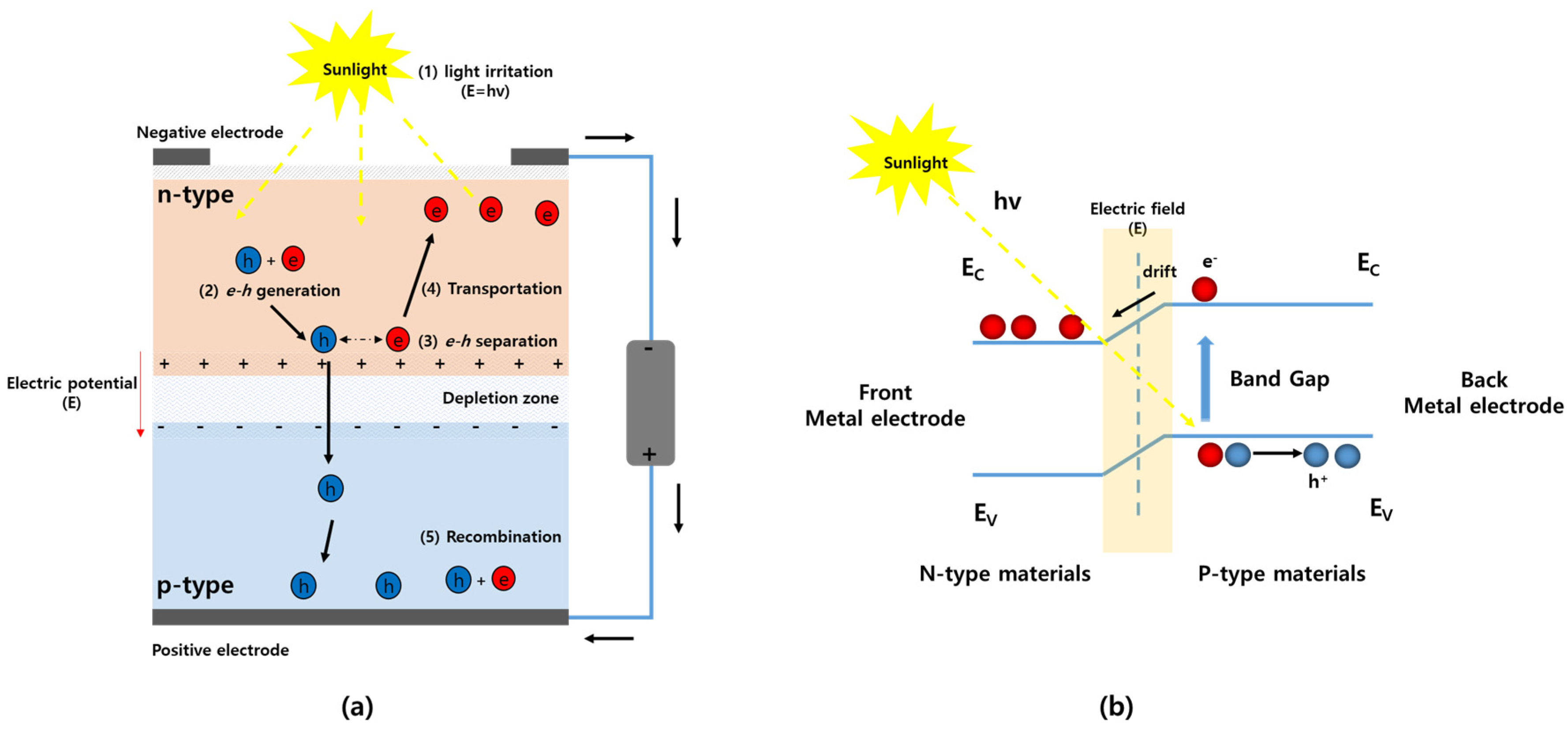
2.1. Basic Photoconversion Mechanism and Structure
- Light absorption and generation of carriers. Photons originating from sunlight arrive at the surface of the solar cell, which absorbs them. Many electron–hole pairs are produced by the photon-absorption mechanism.
- Carrier separation and collection of the light-generated carriers to generate a current. The electrons are released into the negative layer, and the decomposed electrons flow through the positive layer.
- Generation of a voltage across the solar cell. The electrons overcome the boundary energy at the n-type layer and flow through the negative electrode at the top of the cell, which is connected to an external load. This provides a path for the positive material layer; thus, electricity is generated. When the electric field is sufficiently strong to cease further diffusion of holes and electrons, the depleted region reaches equilibrium. Integrating the electric field across the depleted region determines what is called the built-in voltage (also called electric field or voltage). Electrons and holes diffuse into regions with lower concentrations of them.
- Carrier collection and dissipation of power in the load. Electrons return to the cell after exiting the external load and repeatedly move from the positive to the negative side for continuous electricity generation.
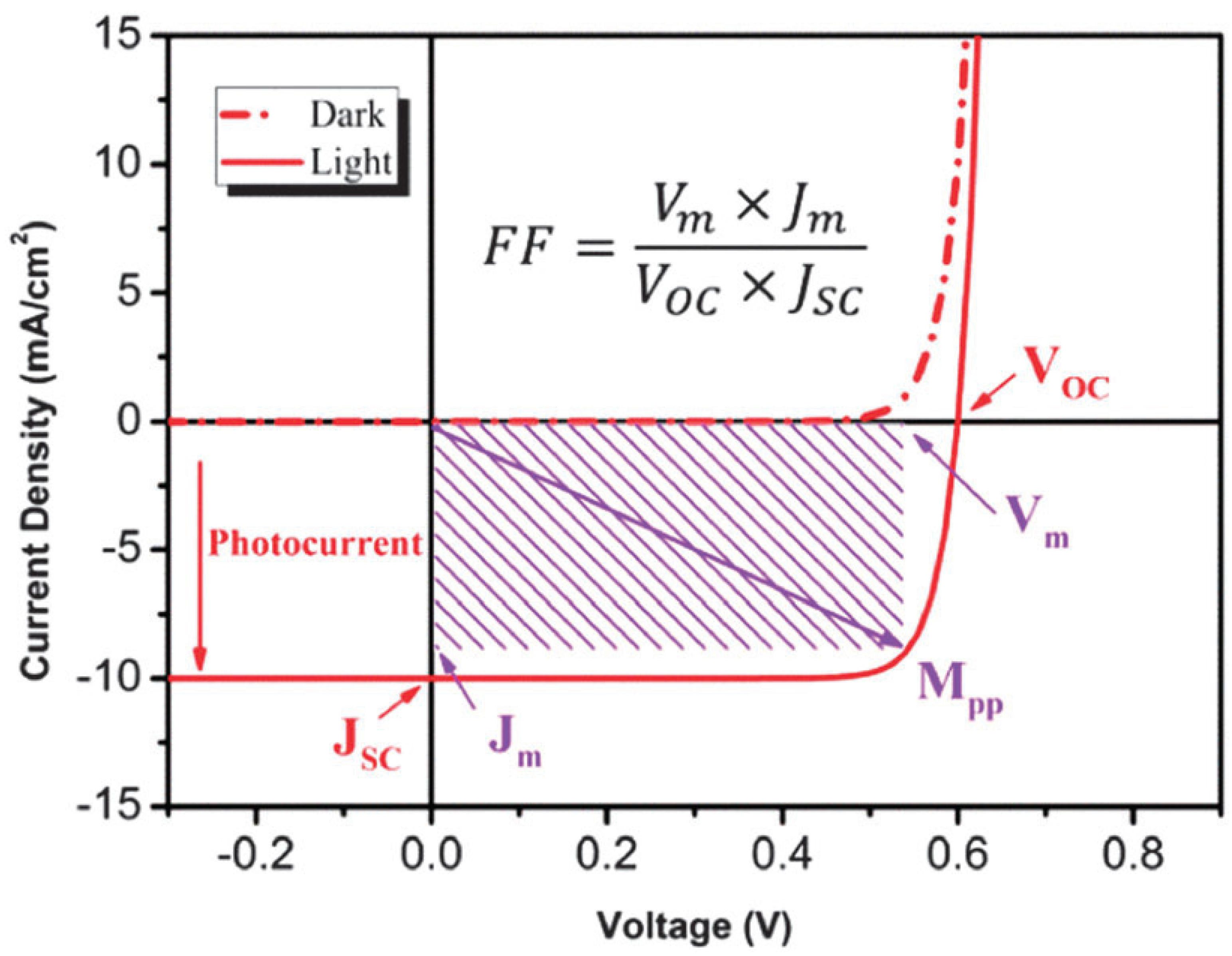
2.2. Performance Evaluation of Solar Cells
- (a)
- Short-Circuit Current (ISC)
- (b)
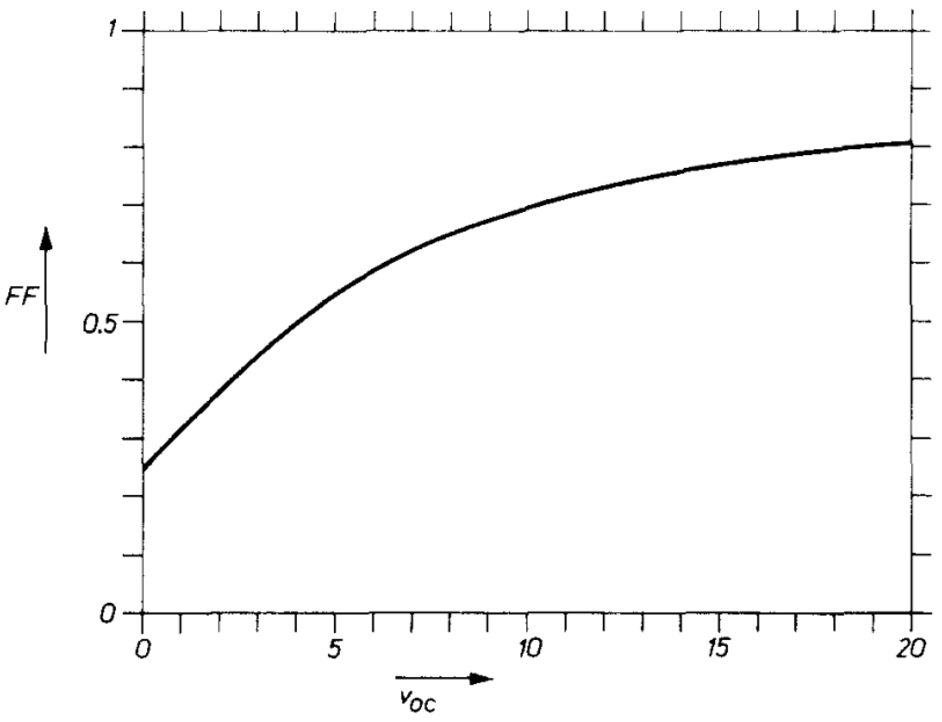
- Fill Factor (FF)
- (c)
- Power-Conversion Efficiency (PCE)
3. Technology for Improving the Power-Conversion Efficiencies
4. Technology of Ultrathin Silicon for Flexible Solar Cells
5. Cell Manufacturing from Materials
5.1. Device Manufacturing Methods
- (a)
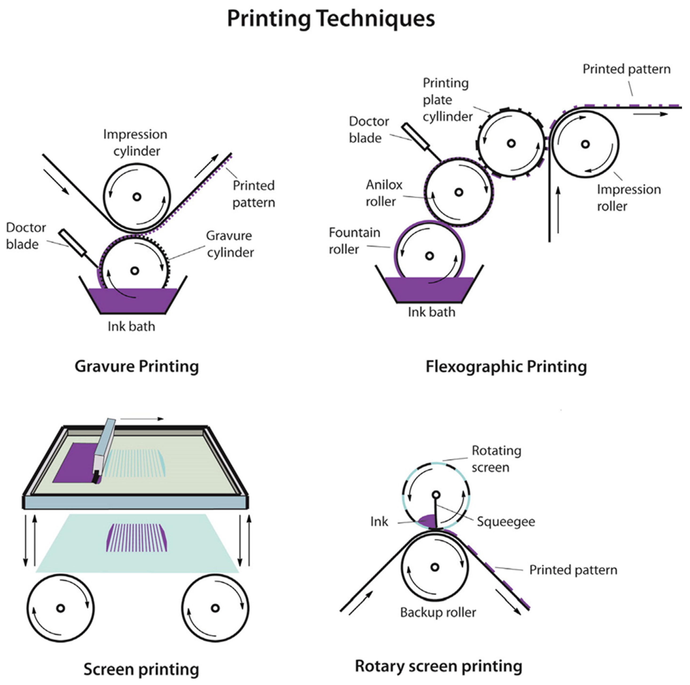
- Roll-to-Roll Printing
- (b)
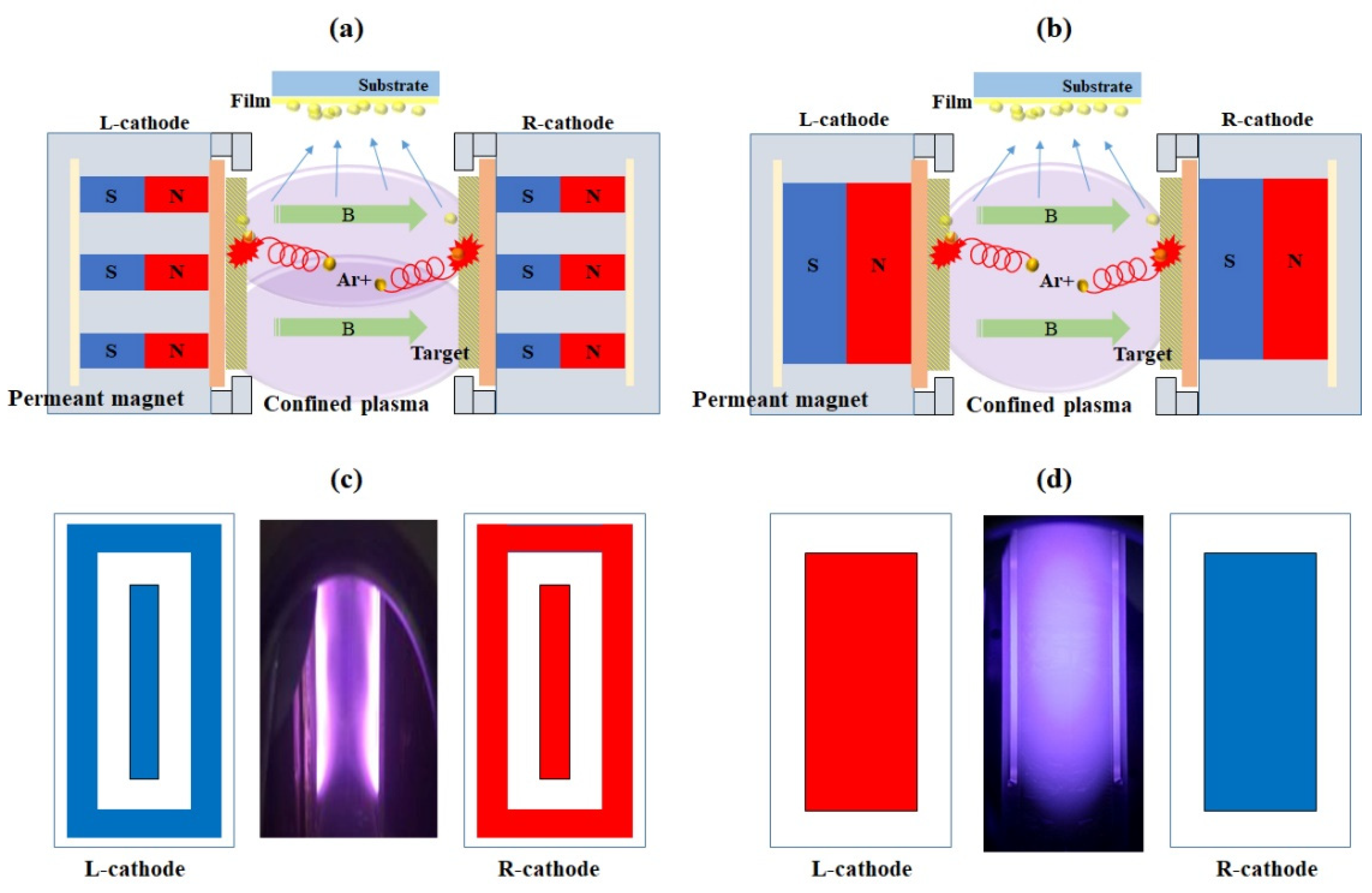
- Sputtering
- (c)
- Spin Coating
- (d)
- Spray Coating
- (e)
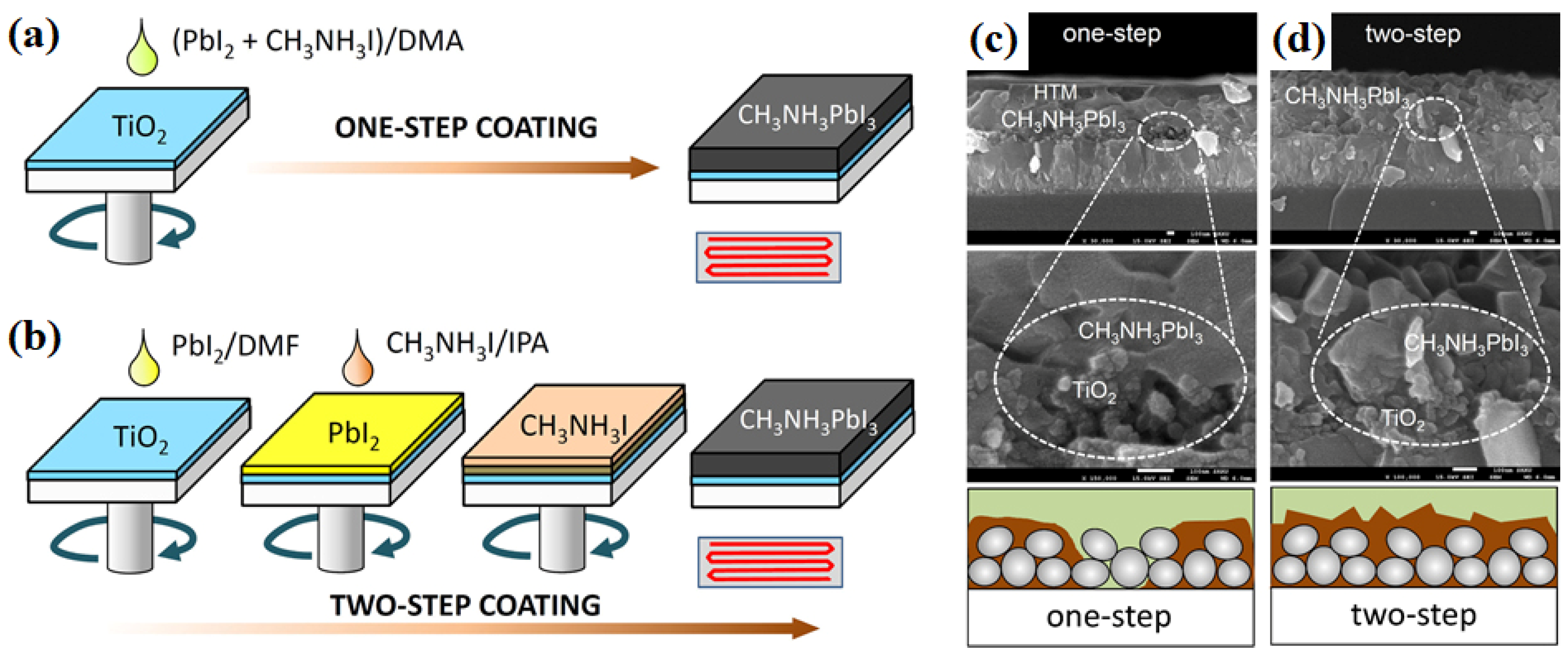
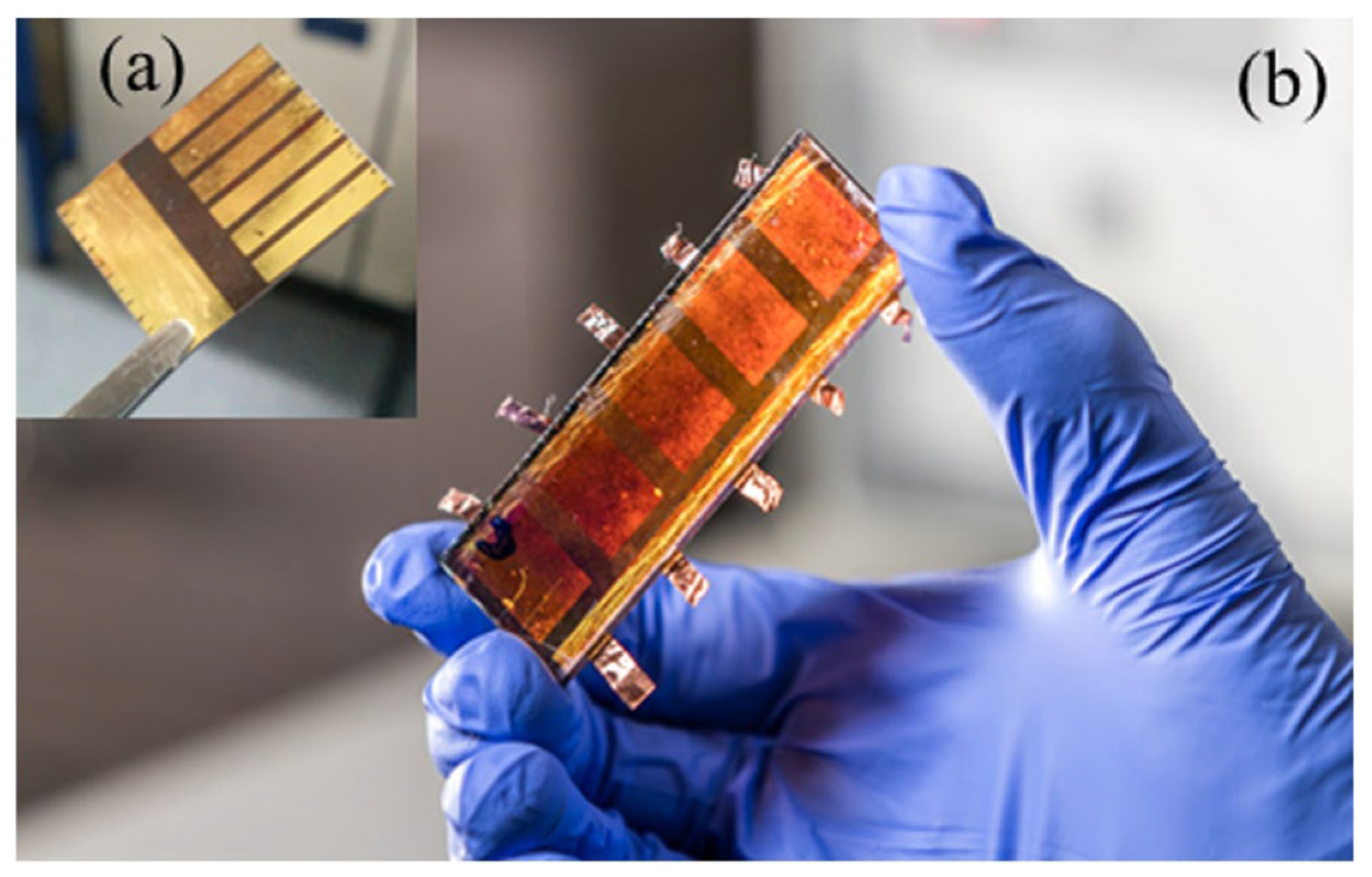
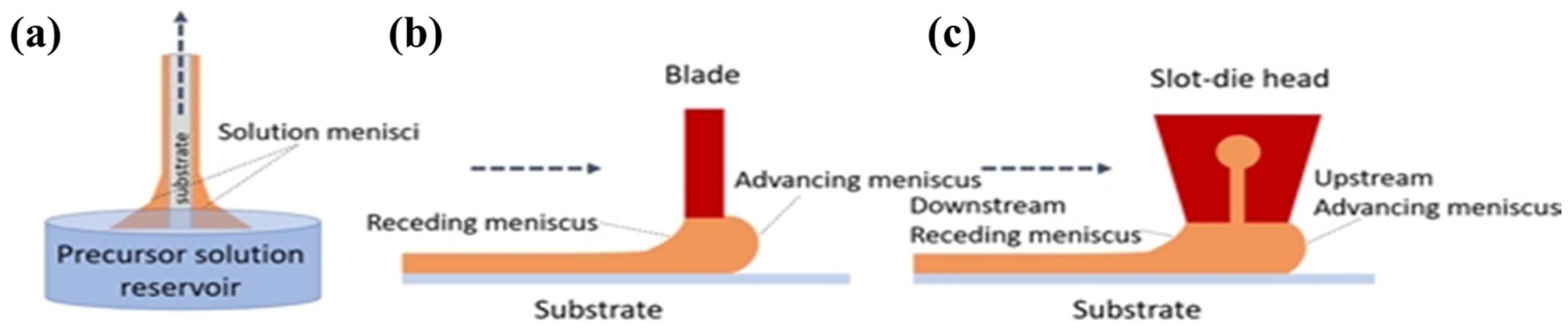
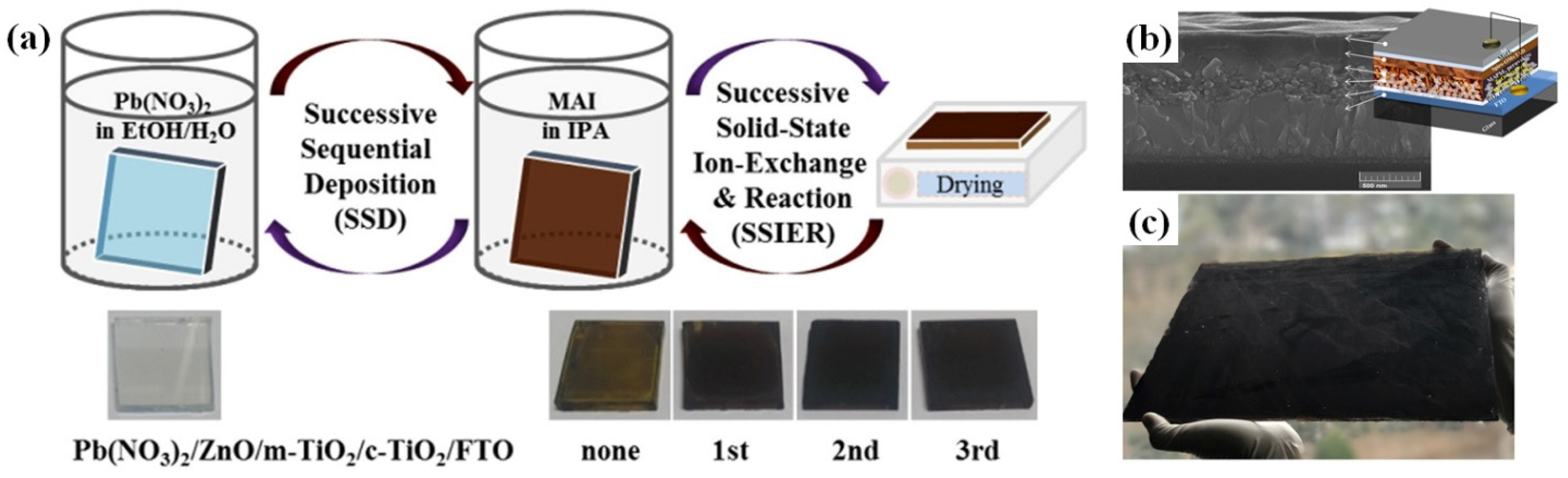
- Other Film-Coating Methods (Dip/Blade/Slot-die)
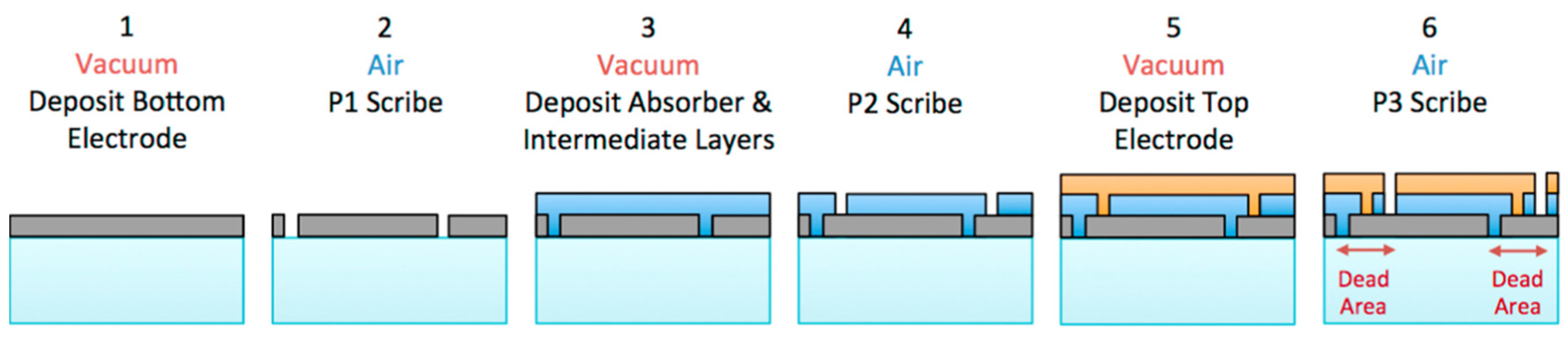
5.2. PV Module Manufacturing: From Cells to Modules
6. Flexible Photovoltaics
6.1. Flexible Thin-Film c-Si Solar Cells
- (a)
- Transfer Technologies
- (b)
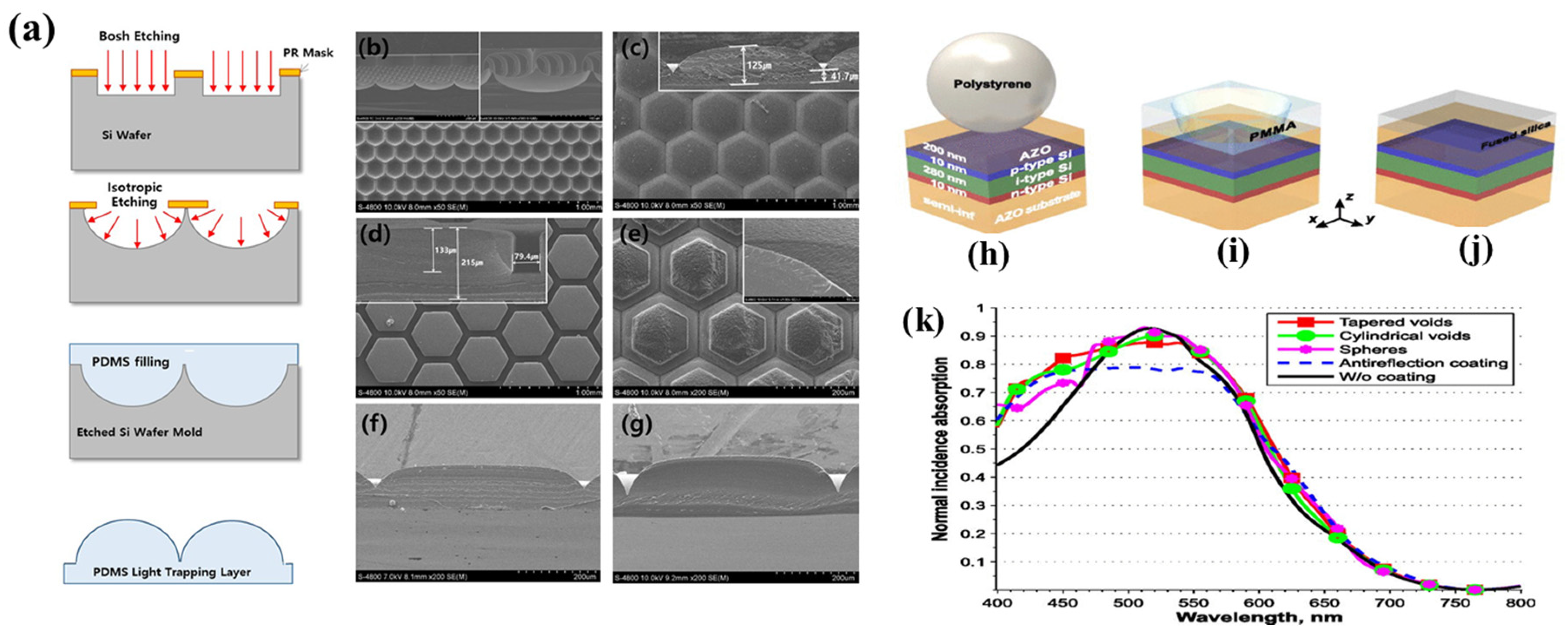
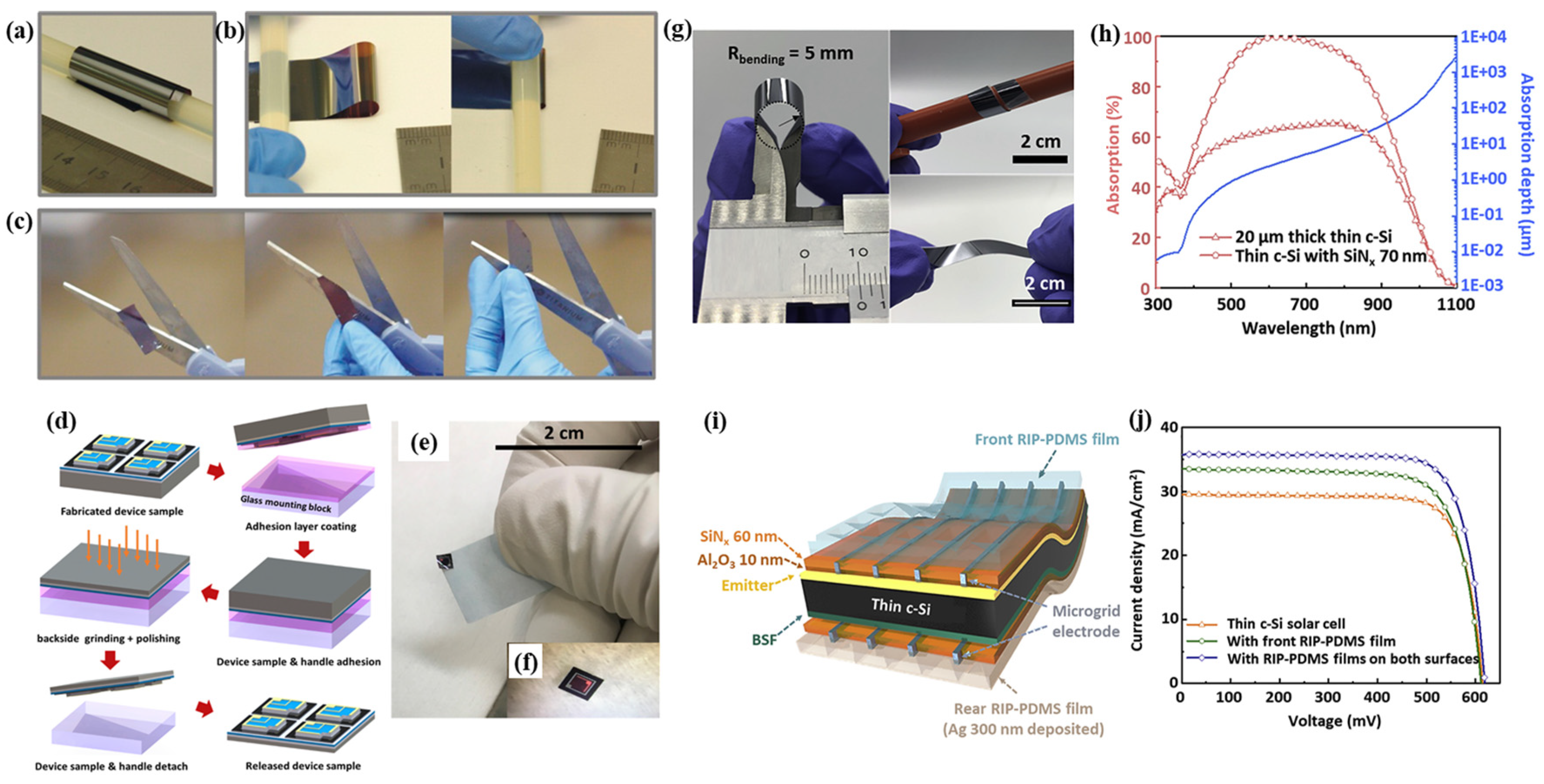
- Etching Method
- (c)
- Exfoliation Method
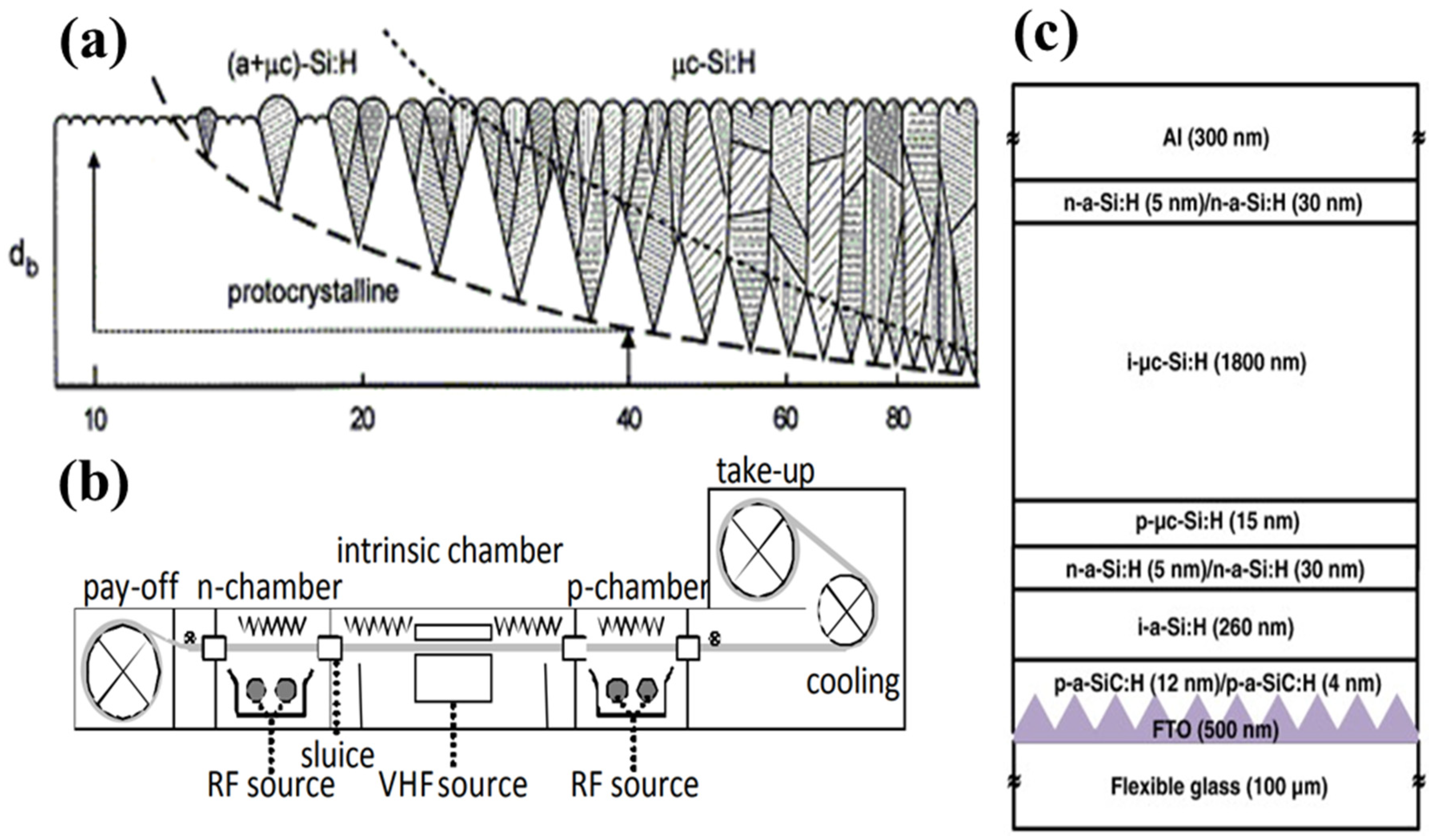
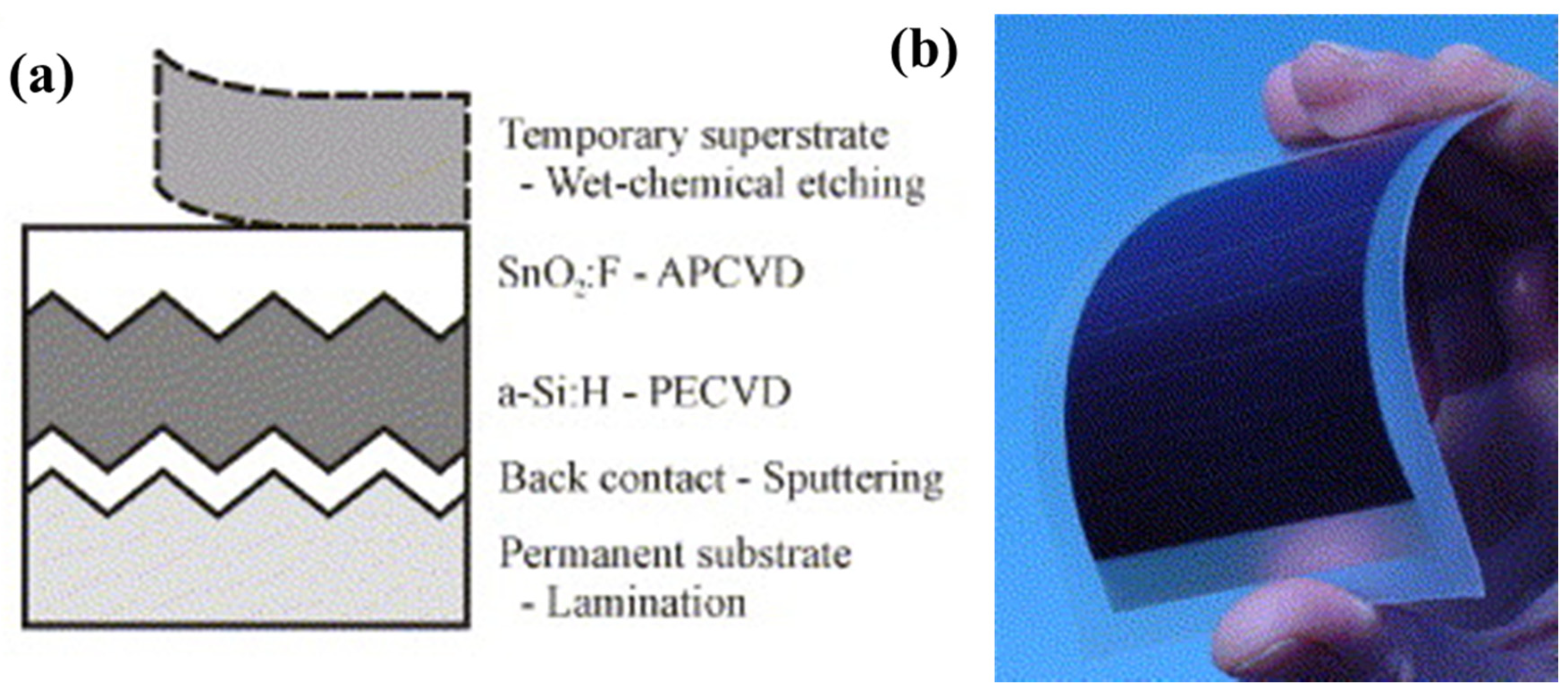
6.2. Flexible Thin-Film a-Si:H/μc-Si:H Solar Cells
- (a)
- Materials of flexible a-Si:H/μc-Si:H solar cells
- (b)
- Structures of flexible a-Si:H/μc-Si:H solar cells
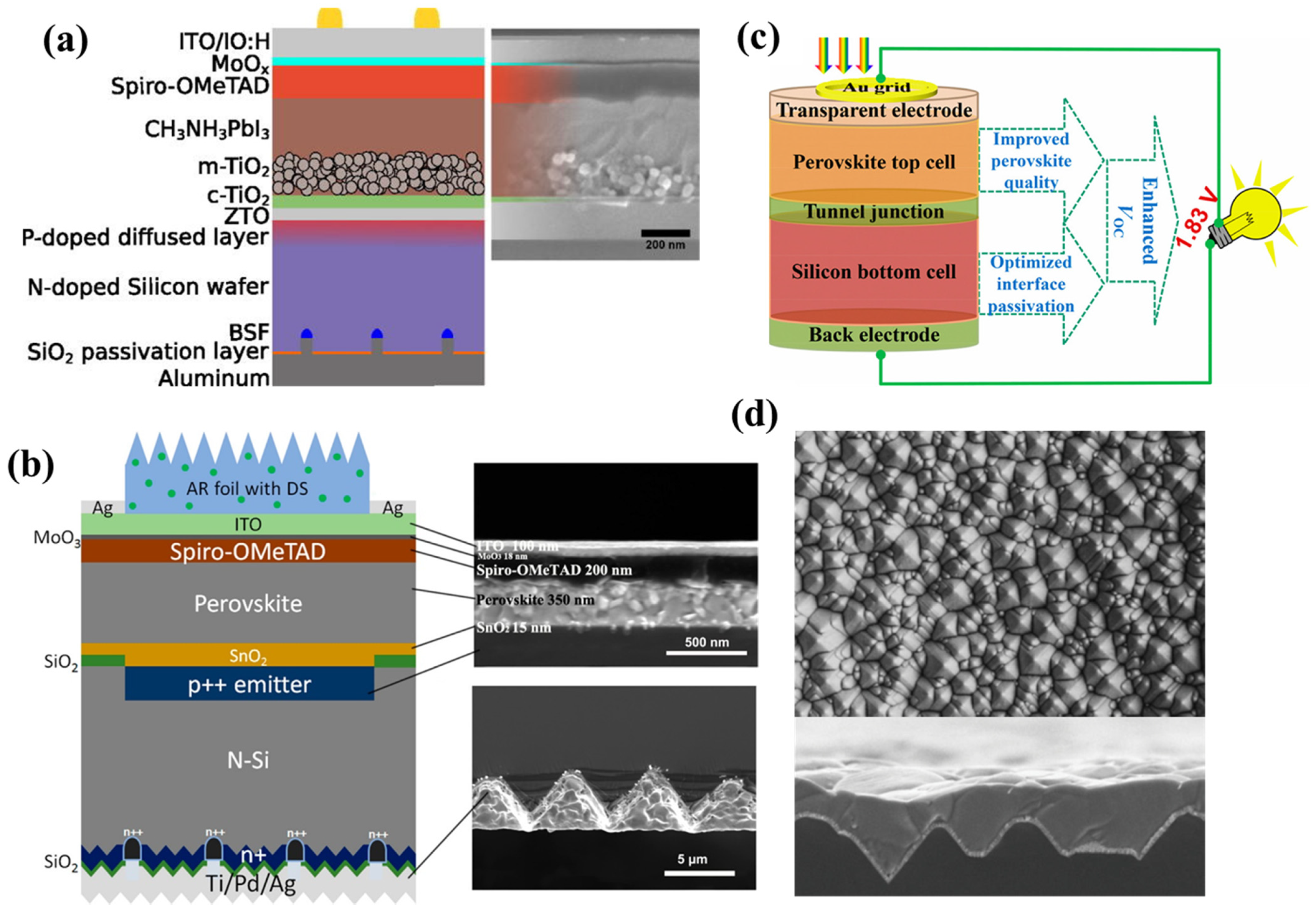
6.3. Perovskite/c-Silicon Tandem Solar Cells
- (a)
- Perovskite/Silicon Homojunction Solar Cells
- (b)
- Perovskite/silicon heterojunction solar cells
7. Conclusions and Outlook
Author Contributions
Funding
Institutional Review Board Statement
Informed Consent Statement
Data Availability Statement
Conflicts of Interest
References
- Wilson, G.M.; Al-Jassim, M.; Metzger, W.K.; Glunz, S.W.; Verlinden, P.; Xiong, G.; Mansfield, L.M.; Stanbery, B.J.; Zhu, K.; Yan, Y. The 2020 photovoltaic technologies roadmap. J. Phys. D Appl. Phys. 2020, 53, 493001. [Google Scholar] [CrossRef]
- Ye, K.-H.; Wang, Z.; Li, H.; Yuan, Y.; Huang, Y.; Mai, W. A novel CoOOH/(Ti, C)-Fe2O3 nanorod photoanode for photoelectrochemical water splitting. Sci. China Mater. 2018, 61, 887–894. [Google Scholar] [CrossRef] [Green Version]
- Chandra, C.; Devina, W.; Cahyadi, H.S.; Kwak, S.K.; Kim, J. Understanding lithium, sodium, and potassium storage mechanisms in silicon oxycarbide. Chem. Eng. J. 2022, 428, 131072. [Google Scholar] [CrossRef]
- Ahmed Abdulkadir, A.; Al-Turjman, F. Smart-grid and Sol. Energy harvesting in the IoT era: An overview. Concurr. Comput. Pract. Exp. 2021, 33, e4896. [Google Scholar] [CrossRef]
- Zhang, J.; Huang, Y.; Lu, X.; Yang, J.; Tong, Y. Enhanced BiVO4 Photoanode Photoelectrochemical Performance via Borate Treatment and a NiFeOx Cocatalyst. ACS Sustain. Chem. Eng. 2021, 9, 8306–8314. [Google Scholar] [CrossRef]
- Da Rosa, A.V.; Ordonez, J.C. Fundamentals of Renewable Energy Processes; Academic Press: Cambridge, MA, USA, 2021. [Google Scholar]
- Moser, R.; Seiler, D.; Huber, H.P.; Marowsky, G. Observation of a spot diameter dependency in confined laser ablation of Zinc Oxide on Copper-Indium-Diselenide. Phys. Procedia 2014, 56, 1034–1040. [Google Scholar] [CrossRef] [Green Version]
- Polman, A.; Knight, M.; Garnett, E.C.; Ehrler, B.; Sinke, W.C. Photovoltaic materials: Present efficiencies and future challenges. Science 2016, 352, 6283. [Google Scholar] [CrossRef] [PubMed] [Green Version]
- Ramanujam, J.; Bishop, D.M.; Todorov, T.K.; Gunawan, O.; Rath, J.; Nekovei, R.; Artegiani, E.; Romeo, A. Flexible CIGS, CdTe and a-Si: H based thin film solar cells: A review. Prog. Mater. Sci. 2020, 110, 100619. [Google Scholar] [CrossRef]
- Pagliaro, M.; Ciriminna, R.; Palmisano, G. Flexible solar cells. ChemSusChem 2008, 1, 880–891. [Google Scholar] [CrossRef] [PubMed]
- Green, M.A. Photovoltaic principles. Physica E 2002, 14, 11–17. [Google Scholar] [CrossRef]
- Markvart, T.; Castañer, L. Principles of solar cell operation. In McEvoy’s Handbook of Photovoltaics; Elsevier: Amsterdam, The Netherlands, 2018; pp. 3–28. [Google Scholar]
- Scully, S.R.; McGehee, M.D. Physics and Materials Issues of Organic Photovoltaics. In Flexible Electronics; Springer: Boston, MA, USA, 2009; pp. 329–371. [Google Scholar]
- Parida, B.; Iniyan, S.; Goic, R. A review of solar photovoltaic technologies. Renew. Sustain. Energy Rev. 2011, 15, 1625–1636. [Google Scholar] [CrossRef]
- Ananda, W. External quantum efficiency measurement of solar cell. In Proceedings of the 2017 15th International Conference on Quality in Research (QiR): International Symposium on Electrical and Computer Engineering, Bali, Indonesia, 24–27 July 2017; pp. 450–456. [Google Scholar]
- De Vos, A. The fill factor of a solar cell from a mathematical point of view. Sol. Cells 1983, 8, 283–296. [Google Scholar] [CrossRef]
- Qi, B.; Wang, J. Fill factor in organic solar cells. Phys. Chem. Chem. Phys. 2013, 15, 8972–8982. [Google Scholar] [CrossRef]
- Yun, M.J.; Sim, Y.H.; Cha, S.I.; Lee, D.Y. omnidirectional Light capture by Solar cells Mimicking the Structures of the epidermal cells of Leaves. Sci. Rep. 2019, 9, 12773. [Google Scholar] [CrossRef] [PubMed] [Green Version]
- Voroshilov, P.M.; Simovski, C.R.; Belov, P.A.; Shalin, A.S. Light-trapping and antireflective coatings for amorphous Si-based thin film solar cells. J. Appl. Phys. 2015, 117, 203101. [Google Scholar] [CrossRef] [Green Version]
- Allen, T.G.; Bullock, J.; Yang, X.; Javey, A.; De Wolf, S. Passivating contacts for crystalline silicon solar cells. Nat. Energy 2019, 4, 914–928. [Google Scholar] [CrossRef]
- Li, X.; Li, P.; Wu, Z.; Luo, D.; Yu, H.-Y.; Lu, Z.-H. Review and perspective of materials for flexible solar cells. Mater. Rep. Energy 2021, 1, 100001. [Google Scholar]
- Hwang, I.; Jeong, Y.; Shiratori, Y.; Park, J.; Miyajima, S.; Yoon, I.; Seo, K. Effective Photon Management of Non-Surface-Textured Flexible Thin Crystalline Silicon Solar Cells. Cell Rep. Phys. Sci. 2020, 1, 100242. [Google Scholar] [CrossRef]
- Xue, M.; Nazif, K.N.; Lyu, Z.; Jiang, J.; Lu, C.-Y.; Lee, N.; Zang, K.; Chen, Y.; Zheng, T.; Kamins, T.I. Free-standing 2.7 μm thick ultrathin crystalline silicon solar cell with efficiency above 12.0%. Nano Energy 2020, 70, 104466. [Google Scholar] [CrossRef]
- Wang, S.; Weil, B.D.; Li, Y.; Wang, K.X.; Garnett, E.; Fan, S.; Cui, Y. Large-area free-standing ultrathin single-crystal silicon as processable materials. Nano Lett. 2013, 13, 4393–4398. [Google Scholar] [CrossRef] [PubMed]
- Salavei, A.; Menossi, D.; Piccinelli, F.; Kumar, A.; Mariotto, G.; Barbato, M.; Meneghini, M.; Meneghesso, G.; Di Mare, S.; Artegiani, E. Comparison of high efficiency flexible CdTe solar cells on different substrates at low temperature deposition. Sol. Energy 2016, 139, 13–18. [Google Scholar] [CrossRef]
- Parashar, P.K.; Kinnunen, S.; Sajavaara, T.; Toppari, J.J.; Komarala, V.K. Thermal atomic layer deposition of AlOxNy thin films for surface passivation of nano-textured flexible silicon. Sol. Energy Mater. Sol. Cells 2019, 193, 231–236. [Google Scholar] [CrossRef]
- Søndergaard, R.; Hösel, M.; Angmo, D.; Larsen-Olsen, T.T.; Krebs, F.C. Roll-to-roll fabrication of polymer solar cells. Mater. Today 2012, 15, 36–49. [Google Scholar] [CrossRef] [Green Version]
- Zardetto, V.; Brown, T.M.; Reale, A.; Di Carlo, A. Substrates for Flexible Electronics: A practical investigation on the electrical, film flexibility, optical, temperature, and solvent resistance properties. J. Polym. Sci. Part B Polym. Phys. 2011, 49, 638–648. [Google Scholar] [CrossRef]
- Kim, S.; Kim, K.H. Effect of magnetic field arrangement of facing targets sputtering (FTS) system on controlling plasma confinement. Coatings 2020, 10, 321. [Google Scholar] [CrossRef] [Green Version]
- Tamagaki, H.; Ikari, Y.; Ohba, N. Roll-to-roll sputter deposition on flexible glass substrates. Surf. Coat. Technol. 2014, 241, 138–141. [Google Scholar] [CrossRef]
- Gerthoffer, A.; Roux, F.; Emieux, F.; Faucherand, P.; Fournier, H.; Grenet, L.; Perraud, S. CIGS solar cells on flexible ultra-thin glass substrates: Characterization and bending test. Thin Solid Films 2015, 592, 99–104. [Google Scholar] [CrossRef]
- Im, J.-H.; Kim, H.-S.; Park, N.-G. Morphology-photovoltaic property correlation in perovskite solar cells: One-step versus two-step deposition of CH3NH3PbI3. Apl Mater. 2014, 2, 081510. [Google Scholar] [CrossRef] [Green Version]
- You, P.; Tang, G.; Yan, F. Two-dimensional materials in perovskite solar cells. Mater. Today Energy 2019, 11, 128–158. [Google Scholar] [CrossRef]
- Kang, S.; Jeong, J.; Cho, S.; Yoon, Y.J.; Park, S.; Lim, S.; Kim, J.Y.; Ko, H. Ultrathin, lightweight and flexible perovskite solar cells with an excellent power-per-weight performance. J. Mater. Chem. A 2019, 7, 1107–1114. [Google Scholar] [CrossRef]
- Uličná, S.; Dou, B.; Kim, D.H.; Zhu, K.; Walls, J.M.; Bowers, J.W.; van Hest, M.F. Scalable deposition of high-efficiency perovskite solar cells by spray-coating. ACS Appl. Energy Mater. 2018, 1, 1853–1857. [Google Scholar] [CrossRef]
- Bishop, J.E.; Mohamad, D.K.; Wong-Stringer, M.; Smith, A.; Lidzey, D.G. Spray-cast multilayer perovskite solar cells with an active-area of 1.5 cm2. Sci. Rep. 2017, 7, 7962. [Google Scholar] [CrossRef] [PubMed]
- Adnan, M.; Lee, J.K. All sequential dip-coating processed perovskite layers from an aqueous lead precursor for high efficiency perovskite solar cells. Sci. Rep. 2018, 8, 2168. [Google Scholar] [CrossRef] [Green Version]
- Dai, X.; Deng, Y.; Van Brackle, C.H.; Huang, J. Meniscus fabrication of halide perovskite thin films at high throughput for large area and low-cost solar panels. Int. J. Extrem. Manuf. 2019, 1, 022004. [Google Scholar] [CrossRef]
- Wang, G.; Adil, M.A.; Zhang, J.; Wei, Z. Large-area organic solar cells: Material requirements, modular designs, and printing methods. Adv. Mater. 2019, 31, 1805089. [Google Scholar] [CrossRef] [PubMed]
- Barugkin, C.; Beck, F.J.; Catchpole, K.R. Diffuse reflectors for improving light management in solar cells: A review and outlook. J. Opt. 2016, 19, 014001. [Google Scholar] [CrossRef]
- Ding, X.; Liu, J.; Harris, T.A. A review of the operating limits in slot die coating processes. AIChE J. 2016, 62, 2508–2524. [Google Scholar] [CrossRef]
- Poortmans, J.; Arkhipov, V. Thin Film Solar Cells: Fabrication, Characterization and Applications; John Wiley & Sons: Hoboken, NJ, USA, 2006; Volume 18, pp. 97–123. [Google Scholar]
- Söderström, T.; Haug, F.-J.; Terrazzoni-Daudrix, V.; Ballif, C. Optimization of amorphous silicon thin film solar cells for flexible photovoltaics. J. Appl. Phys. 2008, 103, 114509. [Google Scholar] [CrossRef]
- Chander, S.; Purohit, A.; Sharma, A.; Nehra, S.; Dhaka, M. Impact of temperature on performance of series and parallel connected mono-crystalline silicon solar cells. Energy Rep. 2015, 1, 175–180. [Google Scholar] [CrossRef] [Green Version]
- Zarmai, M.T.; Ekere, N.; Oduoza, C.; Amalu, E.H. A review of interconnection technologies for improved crystalline silicon solar cell photovoltaic module assembly. Appl. Energy 2015, 154, 173–182. [Google Scholar] [CrossRef]
- Ogbomo, O.O.; Amalu, E.H.; Ekere, N.; Olagbegi, P. Effect of operating temperature on degradation of solder joints in crystalline silicon photovoltaic modules for improved reliability in hot climates. Sol. Energy 2018, 170, 682–693. [Google Scholar] [CrossRef] [Green Version]
- Fields, J.; Pach, G.; Horowitz, K.; Stockert, T.; Woodhouse, M.; van Hest, M.F. Printed interconnects for photovoltaic modules. Sol. Energy Mater. Sol. Cells 2017, 159, 536–545. [Google Scholar] [CrossRef] [Green Version]
- Lucera, L.; Machui, F.; Kubis, P.; Egelhaaf, H.-J.; Brabec, C.J. Highly efficient, large area, roll coated flexible and rigid solar modules: Design rules and realization. In Proceedings of the 2016 IEEE 43rd Photovoltaic Specialists Conference (PVSC), Portland, OR, USA, 5–10 June 2016; pp. 234–237. [Google Scholar]
- Ghosh, A.K.; Fishman, C.; Feng, T. Theory of the electrical and photovoltaic properties of polycrystalline silicon. J. Appl. Phys. 1980, 51, 446–454. [Google Scholar] [CrossRef]
- Goetzberger, A. Optical confinement in thin Si-solar cells by diffuse back reflectors. In Proceedings of the 15th Photovoltaic Specialists Conference, Kissimmee, FL, USA, 12–15 May 1981; pp. 867–870. [Google Scholar]
- Yablonovitch, E.; Cody, G.D. Intensity enhancement in textured optical sheets for solar cells. IEEE Trans. Electron Devices 1982, 29, 300–305. [Google Scholar] [CrossRef]
- Swanson, R.M. A vision for crystalline silicon photovoltaics. Prog. Photovolt. Res. Appl. 2006, 14, 443–453. [Google Scholar] [CrossRef]
- Zhao, J.; Wang, A.; Green, M.A. 24.5% Efficiency silicon PERT cells on MCZ substrates and 24.7% efficiency PERL cells on FZ substrates. Prog. Photovolt. Res. Appl. 1999, 7, 471–474. [Google Scholar] [CrossRef]
- Wang, A.; Zhao, J.; Wenham, S.; Green, M. 21.5% efficient thin silicon solar cell. Prog. Photovolt. Res. Appl. 1996, 4, 55–58. [Google Scholar] [CrossRef]
- Aberle, A.G.; Altermatt, P.P.; Heiser, G.; Robinson, S.J.; Wang, A.; Zhao, J.; Krumbein, U.; Green, M.A. Limiting loss mechanisms in 23% efficient silicon solar cells. J. Appl. Phys. 1995, 77, 3491–3504. [Google Scholar] [CrossRef]
- Werner, J.; Wagner, T.; Gemmer, C.; Berge, C.; Brendle, W.; Schubert, M. Recent progress on transfer-Si solar cells at ipe Stuttgart. In Proceedings of the 3rd World Conference on Photovoltaic Energy Conversion, Osaka, Japan, 11–18 May 2003; pp. 1272–1275. [Google Scholar]
- Rinke, T.J.; Bergmann, R.B.; Werner, J.H. Quasi-monocrystalline silicon for thin-film devices. Appl. Phys. A 1999, 68, 705–707. [Google Scholar] [CrossRef]
- Kimura, M.; Egami, K.; Kanamori, M.; Hamaguchi, T. Epitaxial film transfer technique for producing single crystal Si film on an insulating substrate. Appl. Phys. Lett. 1983, 43, 263–265. [Google Scholar] [CrossRef]
- Nishida, S.; Nakagawa, K.; Iwane, M.; Iwasaki, Y.; Ukiyo, N.; Mizutani, M.; Shoji, T. Si-film growth using liquid phase epitaxy method and its application to thin-film crystalline Si solar cell. Sol. Energy Mater. Sol. Cells 2001, 65, 525–532. [Google Scholar] [CrossRef]
- Solanki, C.S.; Bilyalov, R.R.; Poortmans, J.; Nijs, J.; Mertens, R. Porous silicon layer transfer processes for solar cells. Sol. Energy Mater. Sol. Cells 2004, 83, 101–113. [Google Scholar] [CrossRef]
- Müller, G.; Brendel, R. Simulated Annealing of Porous Silicon. Phys. Status Solidi 2000, 182, 313–318. [Google Scholar] [CrossRef]
- Vitanov, P.; Kamenova, M.; Tyutyundzhiev, N.; Delibasheva, M.; Goranova, E.; Peneva, M. High-efficiency solar cell using a thin porous silicon layer. Thin Solid Films 1997, 297, 299–303. [Google Scholar] [CrossRef]
- Bergmann, R.B.; Werner, J.H. The future of crystalline silicon films on foreign substrates. Thin Solid Films 2002, 403–404, 162–169. [Google Scholar] [CrossRef]
- Schubert, M.B.; Werner, J.H. Flexible solar cells for clothing. Mater. Today 2006, 9, 42–50. [Google Scholar] [CrossRef]
- Feldrapp, K.; Horbelt, R.; Auer, R.; Brendel, R. Thin-film (25.5 μm) solar cells from layer transfer using porous silicon with 32.7 mA/cm2 short-circuit current density. Prog. Photovolt. Res. Appl. 2003, 11, 105–112. [Google Scholar] [CrossRef]
- Sharma, M.; Pudasaini, P.R.; Ruiz-Zepeda, F.; Elam, D.; Ayon, A.A. Ultrathin, flexible organic–inorganic hybrid solar cells based on silicon nanowires and PEDOT:PSS. ACS Appl. Mater. Interfaces 2014, 6, 4356–4363. [Google Scholar] [CrossRef] [PubMed]
- Tang, Q.; Shen, H.; Yao, H.; Gao, K.; Jiang, Y.; Yang, W.; Liu, Y. Cu-assisted chemical etching of bulk c-Si: A rapid and novel method to obtain 45 μm ultrathin flexible c-Si solar cells with asymmetric front and back light trapping structures. Sol. Energy 2018, 170, 263–272. [Google Scholar] [CrossRef]
- Lin, Q.; Huang, H.; Jing, Y.; Fu, H.; Chang, P.; Li, D.; Yao, Y.; Fan, Z. Flexible photovoltaic technologies. J. Mater. Chem. C 2014, 2, 1233–1247. [Google Scholar] [CrossRef]
- Cruz-Campa, J.L.; Okandan, M.; Resnick, P.J.; Clews, P.; Pluym, T.; Grubbs, R.K.; Gupta, V.P.; Zubia, D.; Nielson, G.N. Microsystems enabled photovoltaics: 14.9% efficient 14μm thick crystalline silicon solar cell. Sol. Energy Mater. Sol. Cells 2011, 95, 551–558. [Google Scholar] [CrossRef]
- Bedell, S.W.; Shahrjerdi, D.; Hekmatshoar, B.; Fogel, K.; Lauro, P.A.; Ott, J.A.; Sosa, N.; Sadana, D. Kerf-less removal of Si, Ge, and III–V layers by controlled spalling to enable low-cost PV technologies. IEEE J. Photovolt. 2012, 2, 141–147. [Google Scholar] [CrossRef]
- Rao, R.A.; Mathew, L.; Saha, S.; Smith, S.; Sarkar, D.; Garcia, R.; Stout, R.; Gurmu, A.; Onyegam, E.; Ahn, D.; et al. A novel low cost 25μm thin exfoliated monocrystalline Si solar cell technology. In Proceedings of the 2011 37th IEEE Photovoltaic Specialists Conference, Seattle, WA, USA, 19–24 June 2011; pp. 001504–001507. [Google Scholar]
- Niepelt, R.; Hensen, J.; Steckenreiter, V.; Brendel, R.; Kajari-Schöder, S. Kerfless exfoliated thin crystalline Si wafers with Al metallization layers for solar cells. J. Mater. Res. 2015, 30, 3227–3240. [Google Scholar] [CrossRef] [Green Version]
- Saha, S.; Hilali, M.M.; Onyegam, E.U.; Sarkar, D.; Jawarani, D.; Rao, R.A.; Mathew, L.; Smith, R.S.; Xu, D.; Das, U.K.; et al. Single heterojunction solar cells on exfoliated flexible ~25 μm thick mono-crystalline silicon substrates. Appl. Phys. Lett. 2013, 102, 163904. [Google Scholar] [CrossRef]
- McEvoy, A.; Castaner, L.; Markvart, T. Solar Cells Materials, Manufacture and Operation; Elsevier: Amsterdam, The Netherlands, 2013; pp. 147–216. [Google Scholar]
- Chittick, R.C.; Alexander, J.H.; Sterling, H.F. The preparation and properties of amorphous silicon. J. Electrochem. Soc. 1968, 116, 77–81. [Google Scholar] [CrossRef]
- Carlson, D.E.; Wronski, C.R. Amorphous silicon solar cell. Appl. Phys. Lett. 1976, 28, 671–673. [Google Scholar] [CrossRef]
- Wiesmann, H.; Ghosh, A.K.; McMahon, T.; Strongin, M. A-Si: H produced by high-temperature thermal decomposition of silane. J. Appl. Phys. 1979, 50, 3752–3754. [Google Scholar] [CrossRef] [Green Version]
- Matsumura, H. Study on catalytic chemical vapor deposition method to prepare hydrogenated amorphous silicon. J. Appl. Phys. 1989, 65, 4396–4402. [Google Scholar] [CrossRef]
- Doyle, J.; Robertson, R.; Lin, G.H.; He, M.Z.; Gallagher, A. Production of high-quality amorphous silicon films by evaporative silane surface decomposition. J. Appl. Phys. 1988, 64, 3215–3223. [Google Scholar] [CrossRef]
- Shah, A.; Dutta, J.; Wyrsch, N.; Prasad, K.; Curtins, H.; Finger, F.; Howling, A.; Hollenstein, C. VHF plasma deposition: A comparative overview. MRS Proc. 2011, 258, 15–26. [Google Scholar] [CrossRef]
- Collins, R.W.; Ferlauto, A.S.; Ferreira, G.M.; Chen, C.; Koh, J.; Koval, R.J.; Lee, Y.; Pearce, J.M.; Wronski, C.R. Evolution of microstructure and phase in amorphous, protocrystalline, and microcrystalline silicon studied by real time spectroscopic ellipsometry. Sol. Energy Mater. Sol. Cells 2003, 78, 143–180. [Google Scholar] [CrossRef]
- Merdzhanova, T.; Woerdenweber, J.; Zimmermann, T.; Zastrow, U.; Flikweert, A.J.; Stiebig, H.; Beyer, W.; Gordijn, A. Single-chamber processes for a-Si:H solar cell deposition. Sol. Energy Mater. Sol. Cells 2012, 98, 146–153. [Google Scholar] [CrossRef]
- Platz, R.; Fischer, D.; Dubail, S.; Shah, A. A-Si:H/a-Si:H stacked cell from VHF-deposition in a single chamber reactor with 9% stabilized efficiency. Sol. Energy Mater. Sol. Cells 1997, 46, 157–172. [Google Scholar] [CrossRef] [Green Version]
- Bauer, J.; Calwer, H.; Marklstorfer, P.; Milla, P.; Schulze, F.W.; Ufert, K.D. Manufacturing of large area single junction a-Si:H solar modules with 10.7% efficiency. J. Non-Cryst. Solids 1993, 164–166, 685–688. [Google Scholar] [CrossRef]
- Kroll, U.; Bucher, C.; Benagli, S.; Schönbächler, I.; Meier, J.; Shah, A.; Ballutaud, J.; Howling, A.; Hollenstein, C.; Büchel, A.; et al. High-efficiency p-i-n a-Si:H solar cells with low boron cross-contamination prepared in a large-area single-chamber PECVD reactor. Thin Solid Films 2004, 451–452, 525–530. [Google Scholar] [CrossRef] [Green Version]
- Ballutaud, J.; Bucher, C.; Hollenstein, C.; Howling, A.A.; Kroll, U.; Benagli, S.; Shah, A.; Buechel, A. Reduction of the boron cross-contamination for plasma deposition of p–i–n devices in a single-chamber large area radio-frequency reactor. Thin Solid Films 2004, 468, 222–225. [Google Scholar] [CrossRef]
- Van Aken, B.B.; Devilee, C.; Dörenkämper, M.; Heijna, M.C.; Löffler, J.; Soppe, W.J. Inline processed flexible thin film silicon solar cells using linear PECVD sources. In Proceedings of the 25th European Photovoltaic Solar Energy Conference and Exhibition—5th World Conference on Photovoltaic Energy Conversion, Valencia, Spain, 6–10 September 2010. [Google Scholar]
- Guha, S.; Yang, J.; Pawlikiewicz, A.; Glatfelter, T.; Ross, R.; Ovshinsky, S.R. Band-gap profiling for improving the efficiency of amorphous silicon alloy solar cells. Appl. Phys. Lett. 1989, 54, 2330–2332. [Google Scholar] [CrossRef]
- Yang, J.; Banerjee, A.; Guha, S. Triple-junction amorphous silicon alloy solar cell with 14.6% initial and 13.0% stable conversion efficiencies. Appl. Phys. Lett. 1997, 70, 2975–2977. [Google Scholar] [CrossRef]
- Woerdenweber, J.; Merdzhanova, T.; Zimmermann, T.; Flikweert, A.J.; Stiebig, H.; Beyer, W.; Gordijn, A. Cross-contamination in single-chamber processes for thin-film silicon solar cells. J. Non-Cryst. Solids 2012, 358, 2183–2186. [Google Scholar] [CrossRef]
- Myong, S.Y.; Jeon, L.S.; Kwon, S.W. Superstrate type flexible thin-film Si solar cells using flexible glass substrates. Thin Solid Films 2014, 550, 705–709. [Google Scholar] [CrossRef]
- Van den Donker, M.N.; Gordijn, A.; Stiebig, H.; Finger, F.; Rech, B.; Stannowski, B.; Bartl, R.; Hamers, E.A.G.; Schlatmann, R.; Jongerden, G.J. Flexible amorphous and microcrystalline silicon tandem solar modules in the temporary superstrate concept. Sol. Energy Mater. Sol. Cells 2007, 91, 572–580. [Google Scholar] [CrossRef]
- Shah, A.V.; Schade, H.; Vanecek, M.; Meier, J.; Vallat-Sauvain, E.; Wyrsch, N.; Kroll, U.; Droz, C.; Bailat, J. Thin-film silicon solar cell technology. Prog. Photovolt. Res. Appl. 2004, 12, 113–142. [Google Scholar] [CrossRef]
- Ishikawa, Y.; Schubert, M.B. Flexible protocrystalline silicon solar cells with amorphous buffer layer. Jpn. J. Appl. Phys. 2006, 45, 6812–6822. [Google Scholar] [CrossRef]
- Rath, J.K.; Brinza, M.; Liu, Y.; Borreman, A.; Schropp, R.E.I. Fabrication of thin film silicon solar cells on plastic substrate by very high frequency PECVD. Sol. Energy Mater. Sol. Cells 2010, 94, 1534–1541. [Google Scholar] [CrossRef]
- Ichikawa, Y.; Yoshida, T.; Hama, T.; Sakai, H.; Harashima, K. Production technology for amorphous silicon-based flexible solar cells. Sol. Energy Mater. Sol. Cells 2001, 66, 107–115. [Google Scholar] [CrossRef]
- Takeda, T.; Kondo, M.; Matsuda, A. Thin film silicon solar cells on liquid crystal polymer substrate. In Proceedings of the 3rd World Conference on Photovoltaic Energy Conversion, Osaka, Japan, 11–18 May 2003; pp. 1580–1583. [Google Scholar]
- Yan, B.; Yue, G.; Owens, J.M.; Yang, J.; Guha, S. Over 15% efficient hydrogenated amorphous silicon based triple-junction solar cells incorporating nanocrystalline silicon. In Proceedings of the IEEE 4th World Conference on Photovoltaic Energy Conference, Waikoloa, HI, USA, 7–12 May 2006; pp. 1477–1480. [Google Scholar]
- Lee, C.H.; Kim, D.R.; Cho, I.S.; William, N.; Wang, Q.; Zheng, X. Peel-and-stick: Fabricating thin film solar cell on universal substrates. Sci. Rep. 2012, 2, 1000. [Google Scholar] [CrossRef] [Green Version]
- Nakao, Y.; Hiyama, T. Silicon-based cross-coupling reaction: An environmentally benign version. Chem. Soc. Rev. 2011, 40, 4893–4901. [Google Scholar] [CrossRef]
- Mailoa, J.P.; Bailie, C.D.; Johlin, E.C.; Hoke, E.T.; Akey, A.J.; Nguyen, W.H.; McGehee, M.D.; Buonassisi, T. A 2-terminal perovskite/silicon multijunction solar cell enabled by a silicon tunnel junction. Appl. Phys. Lett. 2015, 106, 121105. [Google Scholar] [CrossRef] [Green Version]
- Werner, J.; Walter, A.; Rucavado, E.; Moon, S.-J.; Sacchetto, D.; Rienaecker, M.; Peibst, R.; Brendel, R.; Niquille, X.; De Wolf, S. Zinc tin oxide as high-temperature stable recombination layer for mesoscopic perovskite/silicon monolithic tandem solar cells. Appl. Phys. Lett. 2016, 109, 233902. [Google Scholar] [CrossRef] [Green Version]
- Wu, Y.; Yan, D.; Peng, J.; Wan, Y.; Phang, S.P.; Shen, H.; Wu, N.; Barugkin, C.; Fu, X.; Surve, S. Monolithic perovskite/silicon-homojunction tandem solar cell with over 22% efficiency. Energy Environ. Sci. 2017, 10, 2472–2479. [Google Scholar] [CrossRef]
- Zheng, J.; Mehrvarz, H.; Liao, C.; Bing, J.; Cui, X.; Li, Y.; Gonçales, V.R.; Lau, C.F.J.; Lee, D.S.; Li, Y. Large-area 23%-efficient monolithic perovskite/homojunction-silicon tandem solar cell with enhanced UV stability using down-shifting material. ACS Energy Lett. 2019, 4, 2623–2631. [Google Scholar] [CrossRef]
- Hou, F.; Yan, L.; Shi, B.; Chen, J.; Zhu, S.; Ren, Q.; An, S.; Zhou, Z.; Ren, H.; Wei, C. Monolithic perovskite/silicon-heterojunction tandem solar cells with open-circuit voltage of over 1.8 V. ACS Appl. Energy Mater. 2019, 2, 243–249. [Google Scholar] [CrossRef]
- Werner, J.; Barraud, L.; Walter, A.; Brauninger, M.; Sahli, F.; Sacchetto, D.; Tétreault, N.; Paviet-Salomon, B.; Moon, S.-J.; Allebé, C. Efficient near-infrared-transparent perovskite solar cells enabling direct comparison of 4-terminal and monolithic perovskite/silicon tandem cells. ACS Energy Lett. 2016, 1, 474–480. [Google Scholar] [CrossRef]
- Bush, K.A.; Palmstrom, A.F.; Zhengshan, J.Y.; Boccard, M.; Cheacharoen, R.; Mailoa, J.P.; McMeekin, D.P.; Hoye, R.L.; Bailie, C.D.; Leijtens, T. 23.6%-efficient monolithic perovskite/silicon tandem solar cells with improved stability. Nat. Energy 2017, 2, 1–7. [Google Scholar] [CrossRef]
- Köhnen, E.; Jošt, M.; Morales-Vilches, A.B.; Tockhorn, P.; Al-Ashouri, A.; Macco, B.; Kegelmann, L.; Korte, L.; Rech, B.; Schlatmann, R. Highly efficient monolithic perovskite silicon tandem solar cells: Analyzing the influence of current mismatch on device performance. Sustain. Energy Fuels 2019, 3, 1995–2005. [Google Scholar] [CrossRef] [Green Version]
- Hou, Y.; Aydin, E.; Bastiani, M.D.; Xiao, C.; Isikgor, F.H.; Xue, D.-J.; Chen, B.; Chen, H.; Bahrami, B.; Chowdhury, A.H.; et al. Efficient tandem solar cells with solution-processed perovskite on textured crystalline silicon. Science 2020, 367, 1135–1140. [Google Scholar] [CrossRef] [PubMed]


Publisher’s Note: MDPI stays neutral with regard to jurisdictional claims in published maps and institutional affiliations. |
© 2021 by the authors. Licensee MDPI, Basel, Switzerland. This article is an open access article distributed under the terms and conditions of the Creative Commons Attribution (CC BY) license (https://creativecommons.org/licenses/by/4.0/).
Share and Cite
Kim, S.; Hoang, V.Q.; Bark, C.W. Silicon-Based Technologies for Flexible Photovoltaic (PV) Devices: From Basic Mechanism to Manufacturing Technologies. Nanomaterials 2021, 11, 2944. https://doi.org/10.3390/nano11112944
Kim S, Hoang VQ, Bark CW. Silicon-Based Technologies for Flexible Photovoltaic (PV) Devices: From Basic Mechanism to Manufacturing Technologies. Nanomaterials. 2021; 11(11):2944. https://doi.org/10.3390/nano11112944
Chicago/Turabian StyleKim, Sangmo, Van Quy Hoang, and Chung Wung Bark. 2021. "Silicon-Based Technologies for Flexible Photovoltaic (PV) Devices: From Basic Mechanism to Manufacturing Technologies" Nanomaterials 11, no. 11: 2944. https://doi.org/10.3390/nano11112944
APA StyleKim, S., Hoang, V. Q., & Bark, C. W. (2021). Silicon-Based Technologies for Flexible Photovoltaic (PV) Devices: From Basic Mechanism to Manufacturing Technologies. Nanomaterials, 11(11), 2944. https://doi.org/10.3390/nano11112944