Article

Effect of Nanostructuring on the Thermoelectric Properties of β-FeSi2

1
ICGM, Univ. Montpellier, CNRS, ENSCM, Montpellier, France
2
CIRIMAT, CNRS, Université de Toulouse, 118 Route de Narbonne, CEDEX 9, 31062 Toulouse, France
3
CNRS-Saint Gobain-NIMS, IRL 3629, Laboratory for Innovative Key Materials and Structures (LINK), National Institute for Materials Science (NIMS), Tsukuba 305-0044, Japan
4
MANA, National Institute for Materials Science (NIMS), 1-1-1 Namiki, Tsukuba 305-0044, Japan
5
Plateforme Nationale CNRS de Frittage Flash, PNF2, MHT, Université Paul-Sabatier, 118 Route de Narbonne, CEDEX 9, 31062 Toulouse, France
*
Authors to whom correspondence should be addressed.
Nanomaterials 2021, 11(11), 2852; https://doi.org/10.3390/nano11112852
Submission received: 6 October 2021 / Revised: 19 October 2021 / Accepted: 21 October 2021 / Published: 26 October 2021
(This article belongs to the Special Issue Nanomaterials for Energy Harvesting)

Abstract

:
Nanostructured β-FeSi2 and β-Fe0.95Co0.05Si2 specimens with a relative density of up to 95% were synthesized by combining a top-down approach and spark plasma sintering. The thermoelectric properties of a 50 nm crystallite size β-FeSi2 sample were compared to those of an annealed one, and for the former a strong decrease in lattice thermal conductivity and an upshift of the maximum Seebeck’s coefficient were shown, resulting in an improvement of the figure of merit by a factor of 1.7 at 670 K. For β-Fe0.95Co0.05Si2, one observes that the figure of merit is increased by a factor of 1.2 at 723 K between long time annealed and nanostructured samples mainly due to an increase in the phonon scattering and an increase in the point defects. This results in both a decrease in the thermal conductivity to 3.95 W/mK at 330 K and an increase in the power factor to 0.63 mW/mK2 at 723 K.

1. Introduction

Global warming and the energy crisis have increased the interest in renewable and green energy sources. Among them, thermoelectricity, which enables the conversion of the loss of heat into electricity, benefits from recent advances thanks to the finding of new families of materials and to the development of new concepts such as multi-scale materials. A thermoelectric material can be characterized by its dimensionless figure of merit ZT = α2σT/λTot, where α is the Seebeck’s coefficient (V/K), σ is the electrical conductivity (S/m) and λTot is the total thermal conductivity (W/mK) combining lattice λL and charge carrier contribution λe [1]. The efficiency of a thermoelectric module is proportional to the figure of merit, consequently, it is expected to reach a high ZT to obtain high performances. However, the efficiency is still limited for the thermogeneration of electricity compared to electricity produced by turbines [2], and most of the new thermoelectric materials, as well as the conventional materials, are made of rare, expensive and toxic elements such as chalcogen or pnictogen atoms or have stability problems [3,4,5]. To overwhelm these last problems, silicide intermetallics such as Mg2Si1-xSnx, higher manganese silicides or β-FeSi2 were developed [6]. This last material has been investigated for several decades for its thermoelectric properties [7]. It crystallizes in the orthorhombic structure Cmce (Space group 64) [8] and is a semiconductor that can be both n or p type with an indirect bandgap around 0.8 eV [9,10,11]. Its power factor α 2 σ is negligible when it is pure and its total thermal conductivity λ Tot ranges from 10 to 18 W/mK at 300 K [11,12]. After alloying with Al or Co, α 2 σ is similar to the best industrial thermoelectric (TE) materials [13] and its maximum figure of merit ZT reaches about 0.2 and 0.4, respectively [7] while it is 1 or greater for the best TE materials [14]. These low ZT values are mainly related to the high value of λTot which is about 6.2 W/mK or 4.3 W/mK at 300 K for Al or Co alloying, respectively [7]. Recently, alloying with both Al and up to 20% of Os leads to an increase in the ZT of p-type β-FeSi2 up to 0.35 [15]. However, the use of Os is expensive and its oxide is very toxic and will limit its applications. Whereas the improvement of α 2 σ can be explained by tuning of the charge carrier concentration, the decrease in λTot can be explained by an increase in the phonon scattering by point defects and mass fluctuations. However, the lattice contribution to the thermal conductivity remains high and still represents >95% of λTot [11]. Thus, there is a large potential for the reduction of thermal conductivity through nanostructuration. In the past, the large efficiency of ball milling for decreasing the crystallite size and so the thermal conductivity was shown. In such conditions, the ZT was increased by about 50% in the best usual thermoelectric materials such as alloys based on Bi2Te3, PbTe or Si-Ge [16,17,18]. An even larger effect was demonstrated in the case of n-doped silicon in which the thermal conductivity was divided by 15 and the ZT increased from 0.2 to 0.7 at 1273 K [19]. We also demonstrated a significant reduction of the thermal conductivity in several transition metal silicides through nanostructuration [20,21,22]. In this study, we investigated the effect of the nanostructuration on thermoelectric properties by combining a top-down approach coupled with Spark Plasma Sintering (SPS) on β-FeSi2 and one of the best Co-alloys β-Fe0.95Co0.05Si2.

2. Materials and Methods

Fe pieces (99.99%, Alfa Aesar, Karlsruhe, Germany), Si lumps (99.9999%, Alfa Aesar, Karlsruhe, Germany) and pre-alloyed CoSi with Co slug (99.95%, Alfa Aesar, Karlsruhe, Germany) were used as raw materials in stoichiometric ratio and melted in an arc-melting furnace under Ar atmosphere. For β-FeSi2 samples, the ingots were first sealed under vacuum in a quartz tube and annealed at 1123K for 50 h whereas β-Fe0.95Co0.05Si2 samples were used as-is. Both β-FeSi2 and β-Fe0.95Co0.05Si2 samples were crushed in an agate mortar and milled in a Fritsch ”Pulverisette 7” planetary micromill (Fritsch, Idar-oberstein, Germany). A silicon nitride container of 45 mL and five 15 mm-diameter balls were used as the milling media with a ball-to-powder mass ratio set to 10:1. The speeds of the supporting disc and the grinding bowl were 510 RPM and 1020 RPM, respectively, for all the experiments (ball acceleration ~80 m s−2). The grinding process was performed in a glovebox under an Ar atmosphere to avoid oxygen contamination. SPS technique was used to prepare dense pellets using a “Dr. sinter 632Lx” unit (Fuji Electronic Industrial Co., Ltd., Tsurugashima, Japan) at PNF2 (Toulouse, France). Tungsten carbide die with an inner diameter of 8 mm was used for those experiments with a graphite foil as a protective and lubricating layer between the samples and the die. Uniaxial pressure in the range 100–500 MPa and DC pulses were both delivered by tungsten carbide punches at both sides. A dwell time of 5 min was applied at a temperature between 873 K and 1073 K. For the Fe0.95Co0.05Si2 sample, the uniaxial pressure was 500 MPa and the sintering temperature was 873 K, the dwell time being still 5 min.
The samples were characterized by powder X-ray diffraction (Philips X’PERT, PANalytical B.V., Amsterdam, The Netherlands). Rietveld refinement with Fullprof or FAULTS software was used for structural analysis of each sample [23,24,25]. The microstructure was analyzed by HRTEM JEOL JEM 2100F (JEOL Ltd., Tokyo, Japan). λ T o t was derived from the thermal diffusivity D measured by the laser flash method from Netzsch (LFA 467 Hyperflash, Netzsch, Selb, Germany), the density d being determined from the Archimedes’ method and the specific heat C p by Pyroceram using the relationship λ T o t = D d C p . The electrical resistivity ρ = 1 / σ and Seebeck’s coefficient were measured using a homemade apparatus.

3. Results and Discussion

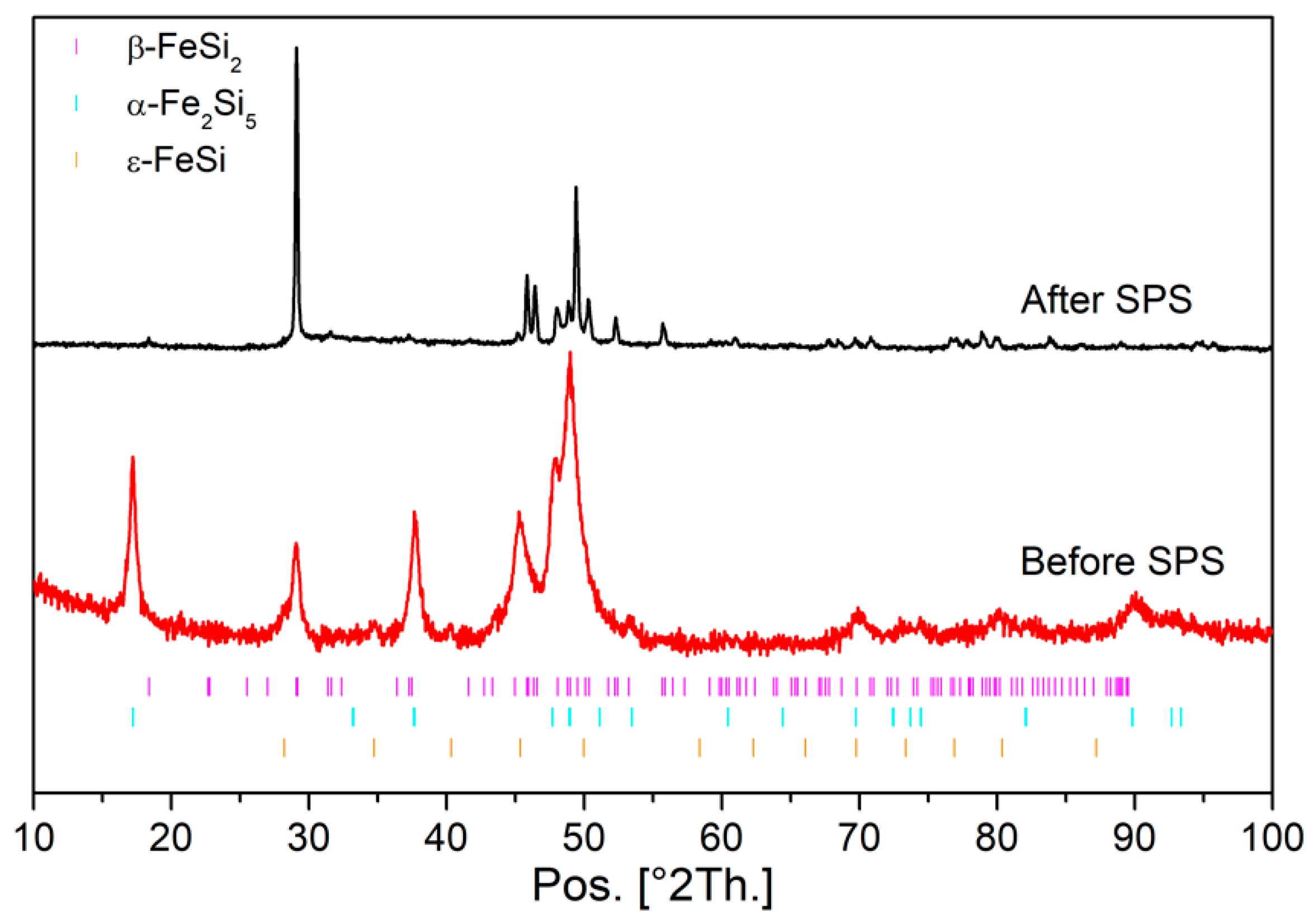
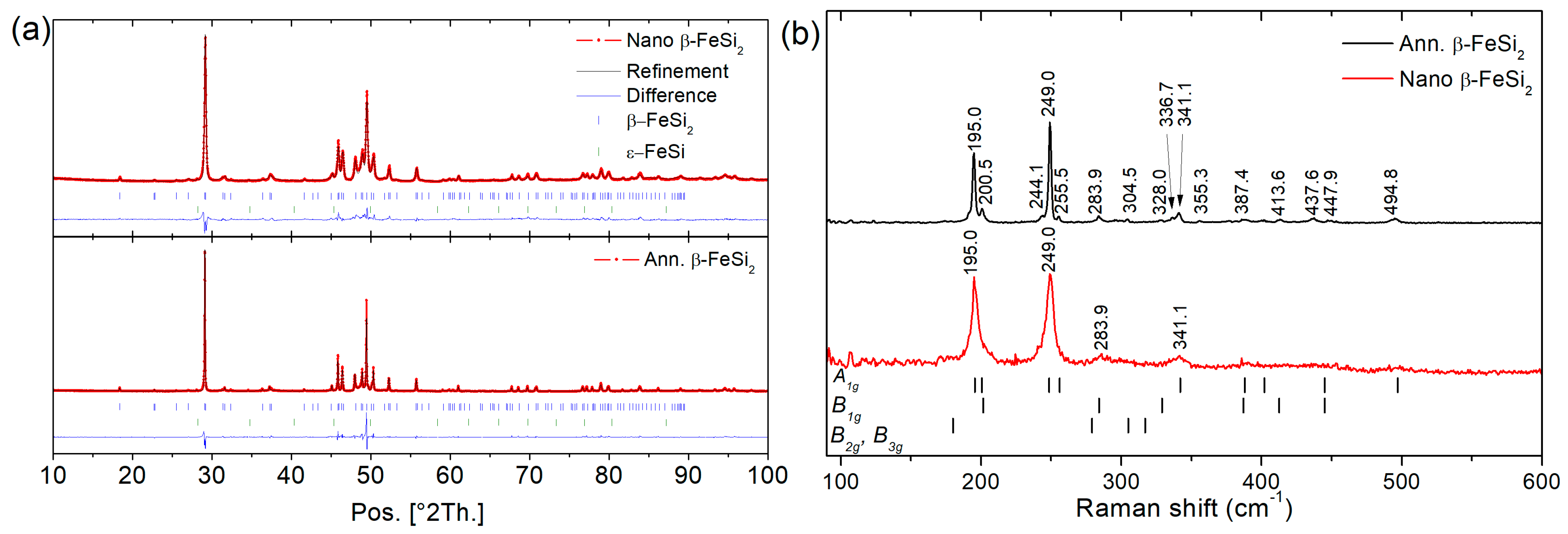
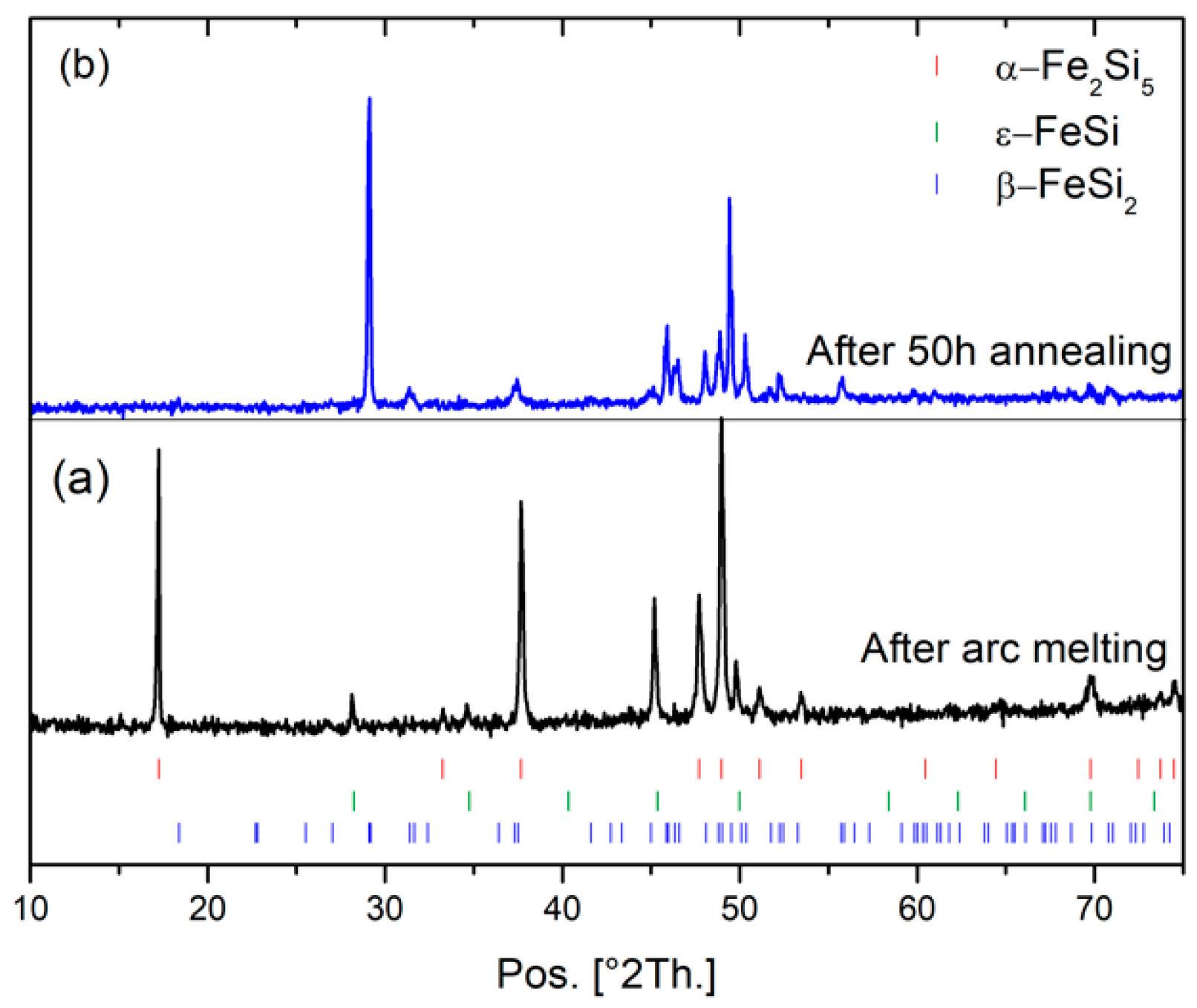
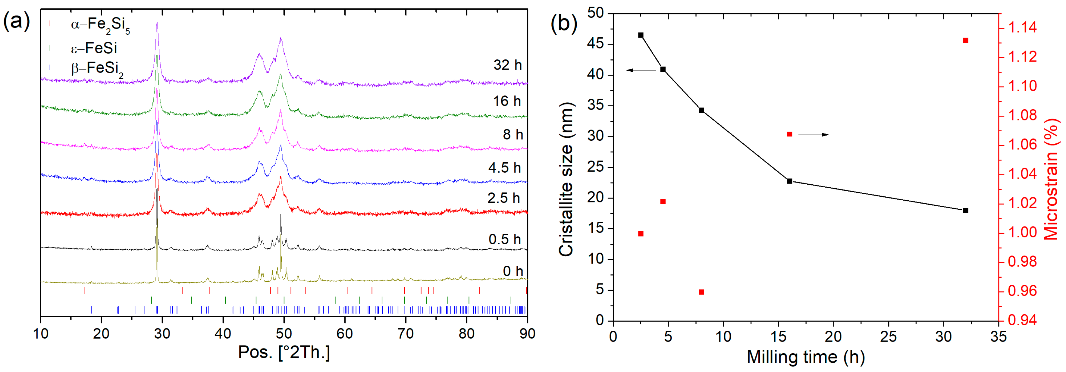
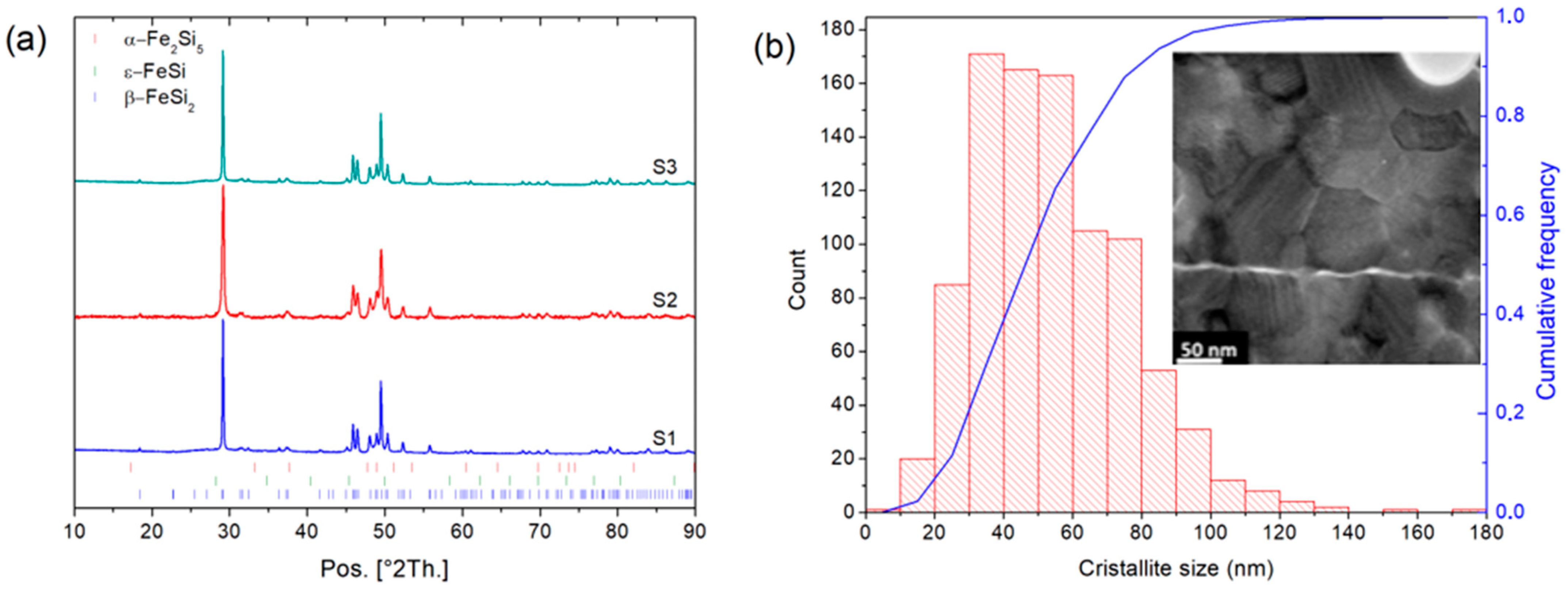
3.1. Structural Analysis

After arc melting of β-FeSi2 samples, the ingots are mainly composed of α-Fe2Si5 and ε-FeSi phases whereas after 50 h of annealing the Rietveld refinement shows that β-FeSi2 is obtained (Figure 1) with a unit cell parameter: a = 9.8767(7) Å, b = 7.8139(4) Å, and c = 7.8296(4) Å, in good agreement with the literature (a = 9.863 Å, b = 7.791 Å, and c = 7.833 Å) [8]. Increasing the milling time from 0.5 h to 32 h was investigated in Figure 2. The analysis of the XRD patterns shows a broadening of the peak feature with increasing the milling time. Rietveld refinement of these data shows a decrease in the crystallite size with increasing the milling time and an increase in the microstrains (Figure 2b). After 8 h of milling, the crystallite size reached ~34 nm and after 32 h of milling, it reached a plateau at ~17 nm. In the next step, the powder sintered by SPS was milled for 8 h, as it is a good compromise between small crystallite size and preparation time. In Table 1, the influence of the sintering conditions (temperature and pressure) on the relative density and the crystallite size of three β-FeSi2 samples (S1, S2 and S3) are summarized. For all samples, the β-FeSi2 phase is evidenced in the XRD patterns (Figure 3).
As expected, an increase in sintering temperature and/or pressure leads to an increase in the relative density. A minimum crystallite size of ~50 nm was obtained at 500 MPa and 873 K for the sample S2 as observed by HRTEM (Figure 3). We also note that an increase in the sintering temperature leads to an increase in the crystallite size, which is typical of grain coarsening. This is why for the sample S4 with five at. % Co on the Fe site, we used the same SPS conditions as for the sample S2, which is the best compromise between high density and small crystallite size. To investigate the effect of the crystallite size on the thermoelectric performances, a pellet S2ann was sintered at 1073 K, 100 MPa for 5 min and annealed for 72 h at 1123 K. S2ann exhibits a crystallite size above 200 nm and a relative density of 93.2%.
After arc melting and mechanical milling of the β-Fe0.95Co0.05Si2 sample, the powder is mainly composed of α-Fe2Si5 and ε-FeSi phases. After SPS of this powder, an in situ reaction occurs leading to β-Fe0.95Co0.05Si2 being obtained (Figure 4). The analysis of the diffraction pattern by Le Bail refinement shows that the unit cell parameters are a = 9.90614(51) Å, b = 7.81260(57) Å, and c = 7.82618(37) Å. The crystallite size reaches 110 nm whereas the microstrain reaches 0.14% slightly above that observed on pure β-FeSi2 samples under these sintering conditions. This could be explained by the in situ reaction which leads to stronger but still limited grain coarsening.

3.2. Lattice Dynamic of Bulk and Nanostructured β-FeSi2

In order to study the effect of the crystallite size on the phonons and their relaxation time, we performed Raman scattering experiments on β-FeSi2 samples S2ann. and S2. β-FeSi2 has an orthorhombic structure of space group Cmce with 24 atoms in the primitive cell and has therefore 69 optical modes and three acoustic modes. The group theory predicts for the Brillouin zone center vibrational modes the following decomposition in irreducible representations [26]:
Γopt = 9Ag ⊕ 9B1g ⊕ 9B2g ⊕ 9B3g ⊕ 9B1u ⊕ 9B2u ⊕ 7B3u ⊕ 8Au and Γac = B1uB2uB3u
There are 36 Raman-active vibrational modes of Ag, B1g, B2g and B3g symmetries and there are 25 Infrared-active vibrational modes of B1u, B2u and B3u.
In Figure 5, we report the Raman spectra of S2ann. and S2 samples. The Raman spectrum extends from about 190 to 500 cm−1 and we found 16 Raman lines for the bulk S2ann. sample and four Raman lines in the nano S2 sample. Our results for the bulk S2ann. sample agree well with previous experimental results [27] and also with the first-principles calculations [26], as illustrated in Figure 5 in which we show the positions of the Raman-active modes assigned from polarized Raman scattering experiments on single crystal [27]. Comparing the Raman spectra of the samples S2ann. and S2, we do not see significant change of the positions of the four main lines but we observe a broadening of the full width at half maximum of all β-FeSi2 assigned modes from 2 cm−1 for the annealed sample S2ann. to 6 cm−1 for the nanostructured sample S2. The broadening of Raman bands could be explained by both the nanostructuration and the increase in defect contents in the crystal structure [28] induced during the mechanical milling. Moreover, this is characteristic of a lower relaxation time [29]. We consequently expect a lower thermal conductivity for nanostructured sample S2. Interestingly, one observes that the amount of stacking fault for samples with 50 nm crystallite size (S2) and 200 nm (S2ann.) are respectively 12% and 19% whereas, in the literature [11], it was observed that it is about 11% for the sample with crystallite size between 0.5 and 1μm and 4 % for crystallite size between 1 to 10 microns. These results show that a decrease in the crystallite size is combined with an increase in the point defect concentration and stacking faults which could also participate in the phonon scattering.

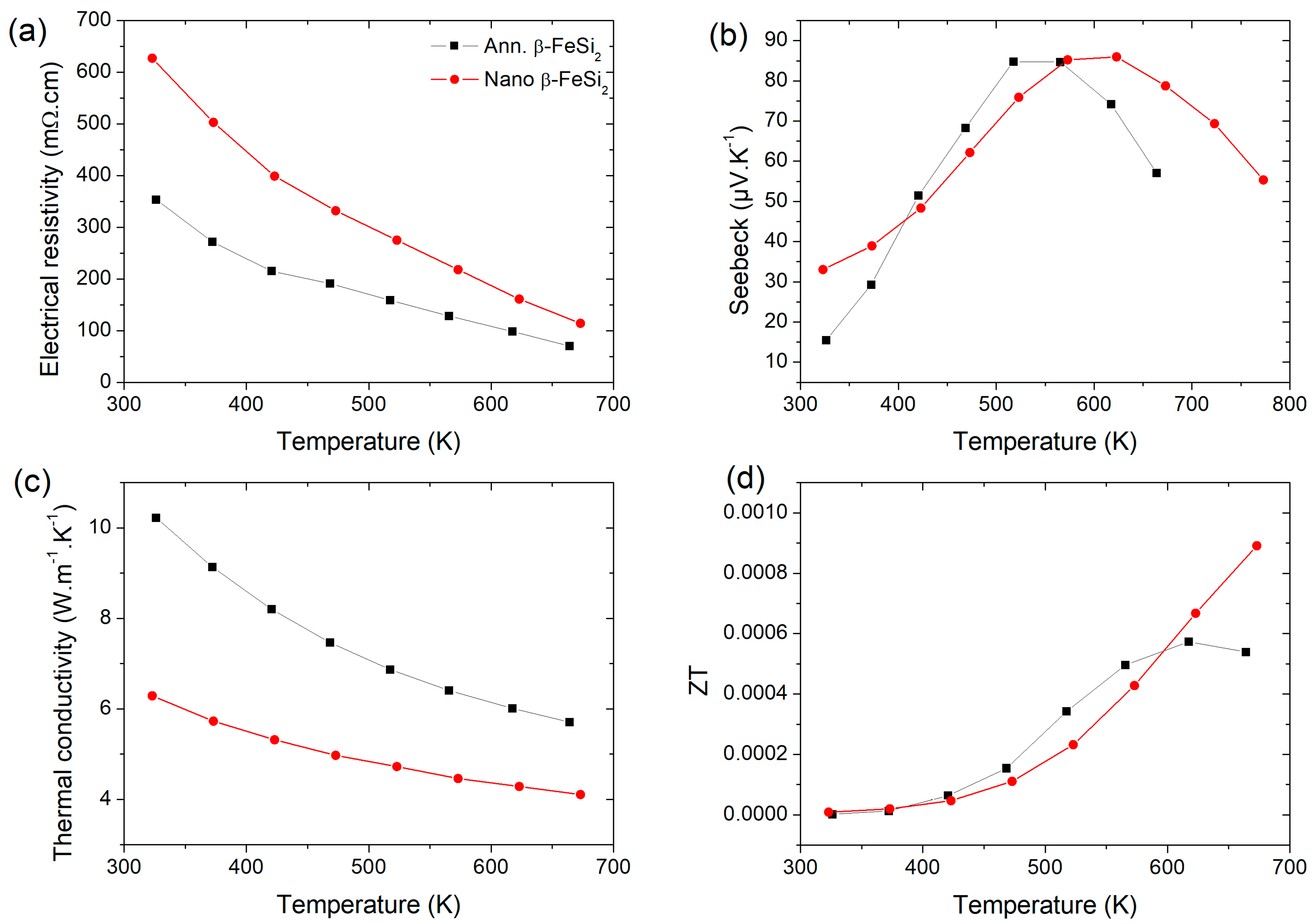
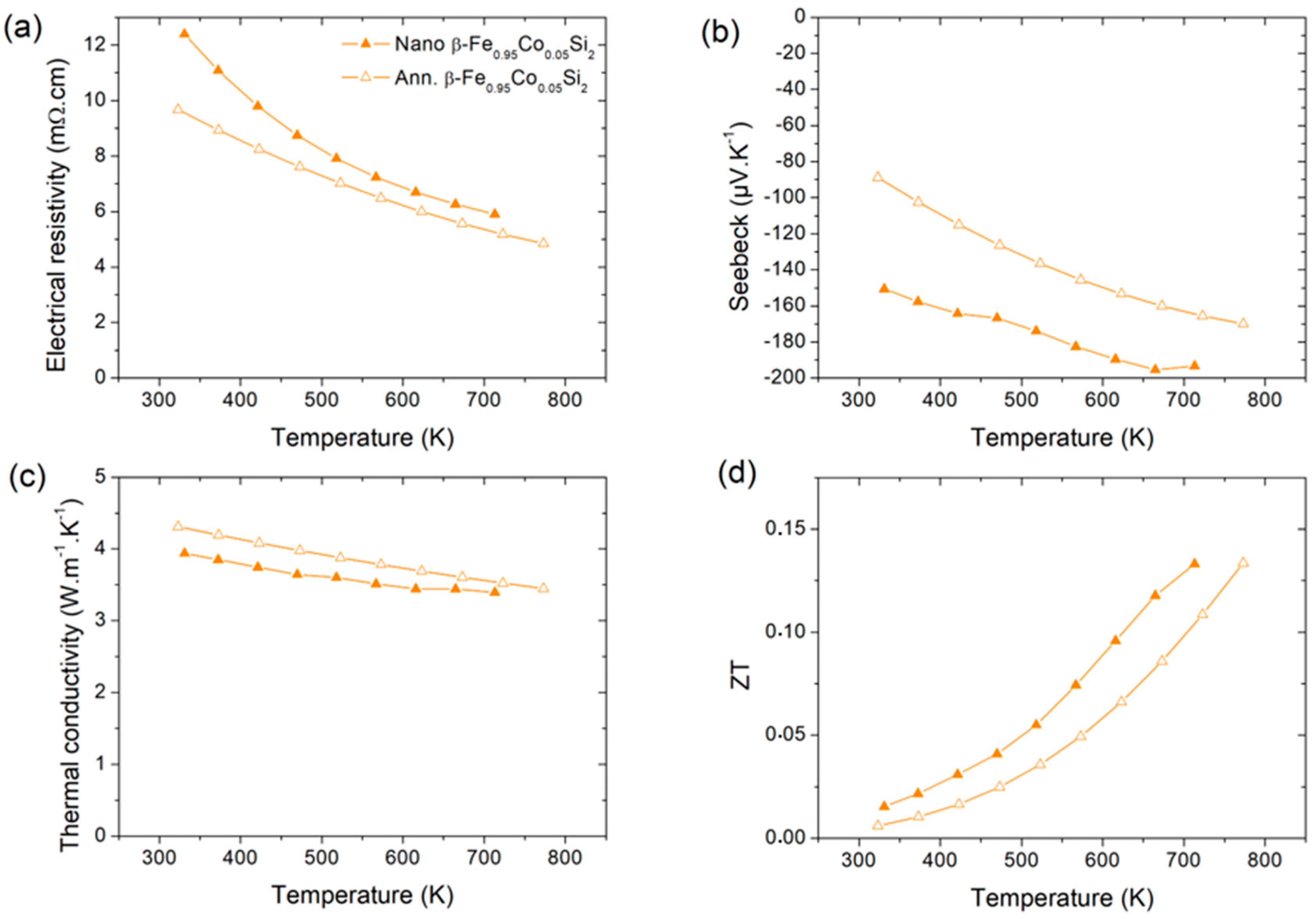
3.3. Thermoelectric Properties

Thermoelectric performances of S2 (after three temperature cycles to 673 K) and S2ann. β-FeSi2 samples are given in Figure 6. Figure 6a presents the decrease in the electrical resistivity of the annealed and nanostructured samples with temperature dependence which is typical of a semi-conductor. The electrical resistivity of the nanostructured sample is higher than the annealed sample due to an increase in electron scattering at the interfaces and by an increase in point defects due to mechanical milling [22]. The Seebeck’s coefficient is quite similar between both samples with a maximum of the thermopower that can be explained either by the change from low temperature extrinsic to high-temperature intrinsic conduction, which is characteristic of a change from heavily doped to lightly doped semiconductor [30] or by bipolar conduction effect as, e.g., in Bi2Te3 based alloys [31,32]. However, the energy bandgap of β-FeSi2 is around 0.8 eV [9,10,11], i.e., about four times larger than in these Bi2Te3 based alloys. This makes it very unlikely to have this effect in β-FeSi2. This is confirmed by the absence of an increase in the thermal conductivity at high temperatures, which is characteristic of bipolar conduction. It is interesting to note that there is an upshift in temperature of the Seebeck maximum when the sample is nanostructured. As both samples were prepared from the same powder, the only parameter that can be changed are defects in the crystal structure. Thus, we explain this upshift by the increase in defect content in the nanostructured sample that broadens the temperature range of the extrinsic regime. Similar weakly positive values of Seebeck’s coefficient were observed for β-FeSi2 by Tani and Kido [33] for samples containing traces of FeSi, i.e., with a deficit of Si probably due to Si vacancies which behave as acceptors, as conformed by DFT calculations [34,35]. The λ T o t , which can be assimilated to the lattice contribution λ L (Figure S1), is decreased by a factor of 1.7 at 300 K and 1.5 at 670 K to reach a λ T o t similar to that of Co-doped samples, as reported earlier [11] (Figure S3) and as observed in Figure 7. This results in an improvement of the figure of merit at 670 K by a factor of 1.7 (Figure 6d) mainly due to the decrease in λ T o t , as the power factor is similar for both samples (Figure S4).
The use of a multi-scale system combining nanostructuring and alloying could then enhance the thermoelectric performances and this can give a good opportunity to improve the performances of β-FeSi2 alloyed with Co. We then studied the case of the thermoelectric properties of the nanostructured β-Fe0.95Co0.05Si2 sample S4 (after six temperature cycles at 723 K) compared to a high temperature annealed sample (S4ann.) for 72 h at 1123 K.
We did not observe any significant variation of the electrical resistivity of the S4 sample after six cycling to 723 K which means that the nanostructure is quite stable up to this temperature for viable application. Consequently, in Figure 7, the results presented correspond only to the last cycle, the details of the cycle are given in SI, Figure S5.
In Figure 7a, the doping of β-FeSi2 with Co has reduced the electrical resistivity by a factor of ~40 for both S4 and S4ann. samples compared to the nanostructured β-FeSi2 (S2) sample and, in Figure 7b, one observes that the Seebeck’s coefficient is also increased. One also observes that the increase in α and ρ is much stronger for nanostructured sample S4. This could be explained by the number of point defects such as p-type Si vacancies which are expected to be higher for nanostructured sample S4 than high temperature annealed one S4ann. Thus, the larger ρ and α should be due to lower charge carrier concentration. This leads to an increase in the power factor by a factor of 1.2 (See Figure S6).
The thermal conductivity is decreased by a factor ~1.5 for S4 and S4ann. compared to S2 leading to an improvement of the figure of merit by a factor ~14. It is slightly lower for the S4 sample and can be explained by the grain coarsening and the decrease in point defects in S4ann. samples which lead to an increase in the phonon relaxation rate [22].
Comparing with the bulk β-Fe0.95Co0.05Si2 samples in the literature, we find a ZT larger than Kim et al. [36] (ZT = 0.09 at 723 K) and similar to that of He et al. [37] (ZT = 0.15 at 723 K) but smaller than Tani et al. [38] (ZT = 0.19 at 723 K) and Hesse et al. [7] (ZT = 0.34 at 723 K). Note that this last result obtained in 1969 has never been reproduced. For all these bulk alloys, the thermal conductivity at 300 K was between 4.3 and 5 W/mK whereas in this study the nanostructured sample reaches 3.95 W/mK. We see therefore that a combination of both alloying and nanostructuring enable λ T o t to decrease again. We find an electrical resistivity larger than the previous works for both S4 and S4ann. samples which could be explained by the nanostructuration of the samples even after annealing. Such behavior has already been observed in the literature [39,40,41] and it is the main issue and challenge for nanostructured samples.
Now, if we compare these data to those from the literature [7,36,37,38,42,43], the gain of ZT is quite limited and shows compensation of the thermoelectric properties (lower λ and lower σ) as observed in previous studies [20,44] on other thermoelectric transition metal silicides. However, it is important to observe that a slight variation of the Co composition can lead to a strong variation of the thermoelectric performances [38] which means that it is important to compare samples from the same batch. Consequently, as observed in Figure 7, the nanostructuring of β-Fe0.95Co0.05Si2 is favorable to an improvement of the figure of merit and further optimization of the Co composition could permit to enhance significantly the figure of merit.

4. Conclusions

High-density nanostructured β-FeSi2 pellets can be successfully obtained from spark plasma sintering highly nanostructured powder. Grain coarsening is strongly limited by working in soft sintering conditions such as 873 K, 500 MPa for 5 min, at which the grain size is 50 nm. The thermoelectric performances of nanostructured undoped β-FeSi2 samples are above those of bulk samples due to a strong decrease in the lattice component of thermal conductivity and an upshift of the maximum Seebeck’s coefficient resulting in an enhancement of the figure of merit by a factor of 1.7 at 670 K. In the case of the nanostructured β-Fe0.95Co0.05Si2 sample, the electrical resistivity and electrical conductivity are strongly decreased compared to the nanostructured undoped β-FeSi2 samples but the electrical resistivity is higher than in the bulk β-Fe0.95Co0.05Si2 which is not fully compensated by the 10–20% reduction of the thermal conductivity in the nanostructured samples compared to the bulk samples, resulting in ZT = 0.14 at 723 K. This must be due to the smaller mean-free path of the phonons compared to the electrons in β-Fe0.95Co0.05Si2.

Supplementary Materials

The following are available online at https://www.mdpi.com/article/10.3390/nano11112852/s1, Figure S1: Temperature dependence of the total thermal conductivity, λ T o t , of annealed (S2ann.) and nanostructured (S2) samples. The electronic component of the thermal conductivity, λ e , was determined assuming that L = L 0 , Figure S2: Temperature dependence of the total thermal conductivity, λ T o t , of annealed (S4ann.) and nanostructured (S4) samples. The electronic component of the thermal conductivity, λ_e, was determined assuming that L = L 0 , Figure S3: Thermal conductivity of nanostructured S2 and annealed S2ann. samples compared to the literature data [S1], Figure S4: Temperature dependence of the power factor of annealed (S2ann.) and nanostructured (S2) samples, Figure S5: Temperature dependence of the electrical resistivity of S4 sample after six heating to 723 K, Figure S6: Temperature dependence of the power factor of annealed (S4ann.) and nanostructured (S4) SPS samples. Table S1: Structural parameters and stacking faults probability (SF) of nanostructured β-FeSi2 (S2), annealed β-FeSi2 (S2ann.) and β-FeSi2 from the literature data [S1] using FAULTS.

Author Contributions

Conceptualization, L.A., D.M., C.E., E.F., R.V. and M.B.; methodology L.A., D.M., C.E., E.F., R.V. and M.B.; formal analysis, L.A., B.S., S.L.T., D.B., T.M., R.V. and M.B.; investigation, L.A., D.M., B.S., S.L.T., D.B., T.M., C.E., E.F., R.V. and M.B.; resources, D.M., T.M., L.C., G.C., C.E., E.F., R.V. and M.B.; writing—original draft preparation, L.A., R.V. and M.B.; writing—review and editing, L.A., D.M., B.S., S.L.T., D.B., T.M., C.E., E.F., R.V. and M.B.; project administration, E.F. and M.B.; funding acquisition, E.F. and M.B. All authors have read and agreed to the published version of the manuscript.

Funding

This research was funded by Chimie Balard Cirimat Carnot Institute through the ANR program, grant number N°16 CARN 0008-01.

Data Availability Statement

Data is contained within the article or Supplementary Materials.

Acknowledgments

The authors would like to thank the Chimie Balard Cirimat Carnot Institute for supporting the ECO-ThermoELEC project, the “centre de microcaractérisation Raimond Castaing” (Toulouse) for HRTEM analysis and A. Vieira E. Silva for its technical support. B.S thanks JSPS for the postdoctoral fellowship (P19720).

Conflicts of Interest

The authors declare no conflict of interest.

References

  1. Goldsmid, H.J. Thermoelectric Refrigeration; Springer: Boston, MA, USA, 1964. [Google Scholar]
  2. Vining, C.B. An inconvenient truth about thermoeletrics. Nat. Mater. 2009, 8, 83–85. [Google Scholar] [CrossRef] [PubMed]
  3. Amatya, R.; Ram, R.J. Trend for thermoelectric materials and their earth abundance. J. Electron. Mater. 2012, 41, 1011–1019. [Google Scholar] [CrossRef]
  4. Muchtar, A.R.; Srinivasan, B.; le Tonquesse, S.; Singh, S.; Soelami, N.; Yuliarto, B.; Berthebaud, D.; Mori, T. Physical insights on the lattice softening driven mid-temperature range thermoelectrics of Ti/Zr-inserted SnTe—An outlook beyond the horizons of conventional phonon scattering and excavation of Heikes’ equation for estimating carrier properties. Adv. Energy Mater. 2021, 11, 2101122. [Google Scholar] [CrossRef]
  5. Srinivasan, B.; le Tonquesse, S.; Gellé, A.; Bourgès, C.; Monier, L.; Ohkubo, I.; Halet, J.F.; Berthebaud, D.; Mori, T. Screening of transition (Y, Zr, Hf, V, Nb, Mo, and Ru) and rare-earth (La and Pr) elements as potential effective dopants for thermoelectric GeTe—An experimental and theoretical appraisal. J. Mater. Chem. A 2020, 8, 19805–19821. [Google Scholar] [CrossRef]
  6. Fedorov, M.I.; Isachenko, G.N. Silicides: Materials for thermoelectric energy conversion. Jpn. J. Appl. Phys. 2015, 54, 07JA05. [Google Scholar] [CrossRef] [Green Version]
  7. Hesse, J. Leistungsthermoelemente aus Eisendisilicid fur die Stromerzeugung (Power thermocouples made of iron disilicide for power generation). Z. Fur Angew. Phys. 1969, 28, 133. [Google Scholar]
  8. Dusausoy, Y.; Protas, J.; Wandji, R.; Roques, B. Structure cristalline du disiliciure de fer, FeSi2β (cristalline structure of iron disilicide, FeSi2β). Acta Crystallogr. Sect. B Struct. Crystallogr. Cryst. Chem. 1971, 27, 1209–1218. [Google Scholar] [CrossRef]
  9. Christensen, N.E. Electronic structure of β-FeSi2. Phys. Rev. B 1990, 42, 7148–7153. [Google Scholar] [CrossRef] [PubMed]
  10. Udono, H.; Kikuma, I.; Okuno, T.; Masumoto, Y.; Tajima, H. Indirect optical absorption of single crystalline β-FeSi2. Appl. Phys. Lett. 2004, 85, 1937–1939. [Google Scholar] [CrossRef] [Green Version]
  11. le Tonquesse, S.; Verastegui, Z.; Huynh, H.; Dorcet, V.; Guo, Q.; Demange, V.; Prestipino, C.; Berthebaud, D.; Mori, T.; Pasturel, M. Magnesioreduction synthesis of Co-Doped β-FeSi2: Mechanism, microstructure, and improved thermoelectric properties. ACS Appl. Energy Mater. 2019, 2, 8525–8534. [Google Scholar] [CrossRef]
  12. Ito, M.; Nagai, H.; Oda, E.; Katsuyama, S.; Majima, K. Effects of P doping on the thermoelectric properties of β-FeSi2. J. Appl. Phys. 2002, 91, 2138–2142. [Google Scholar] [CrossRef]
  13. Rowe, D.M. Thermoelectrics Handbook: Macro to Nano; CRC: Boca Raton, FL, USA; Taylor & Francis: Abingdon, UK, 2006. [Google Scholar]
  14. Liu, Z.; Sato, N.; Gao, W.; Yubuta, K.; Kawamoto, N.; Mitome, M.; Kurashima, K.; Owada, Y.; Nagase, K.; Lee, C.H.; et al. Demonstration of ultrahigh thermoelectric efficiency of ∼7.3% in Mg3Sb2/MgAgSb module for low-temperature energy harvesting. Joule 2021, 5, 1196–1208. [Google Scholar] [CrossRef]
  15. Du, X.; Qiu, P.; Chai, J.; Mao, T.; Hu, P.; Yang, J.; Sun, Y.-Y.; Shi, X.; Chen, L. Doubled thermoelectric figure of merite in p-type β-FeSi2-via synergistically optimizing electrical and thermal transports. ACS Appl. Mater. Interfaces 2020, 12, 12901–12909. [Google Scholar] [CrossRef]
  16. Heremans, J.P.; Dresselhaus, M.S.; Bell, L.E.; Morelli, D.T. When thermoelectrics reached the nanoscale. Nat. Nanotech. 2013, 8, 471–473. [Google Scholar] [CrossRef] [PubMed]
  17. Poudel, B.; Hao, Q.; Ma, Y.; Lan, Y.; Minnich, A.; Yu, B.; Yan, X.; Wang, D.; Muto, A.; Vashaee, D.; et al. High-thermoelectric performance of nanostructured bismuth antimonide telluride bulk alloys. Science 2008, 320, 634–638. [Google Scholar] [CrossRef] [PubMed] [Green Version]
  18. Joshi, G.; Lee, H.; Lan, Y.; Wang, X.; Zhu, G.; Wang, D.; Gould, R.W.; Cuff, D.C.; Tang, M.Y.; Dresselhaus, M.S.; et al. Enhanced thermoelectric figure of merit in nanostructured p-type silicon germanium bulk alloys. Nano Lett. 2008, 8, 4670–4674. [Google Scholar] [CrossRef] [PubMed]
  19. Bux, S.K.; Blair, R.G.; Gogna, P.K.; Lee, H.; Chen, G.; Dresselhaus, M.S.; Kaner, R.B.; Fleurial, J.-P. Nanostructured bulk silicon as an effective thermoelectric material. Adv. Funct. Mater. 2009, 19, 2445–2452. [Google Scholar] [CrossRef]
  20. Longhin, M.; Viennois, R.; Ravot, D.; Robin, J.-J.; Villeroy, B.; Vaney, J.-B.; Candolfi, C.; Lenoir, B.; Papet, P. Nanostructured CoSi obtained by spark plasma sintering. J. Electron. Mater. 2015, 44, 1963–1966. [Google Scholar] [CrossRef]
  21. Khalil, M. Investigation and Optimization of Semiconducting Chromium Disilicide Based Materials for Thermoelectric Applications. Ph.D. Thesis, University of Montpellier, Montpellier, France, 2015. [Google Scholar]
  22. Khalil, M.; Moll, A.; Godfroy, M.; Letrouit-Lebranchu, A.; Villeroy, B.; Alleno, E.; Viennois, R.; Beaudhuin, M. Thermoelectric properties and stability of nanostructured chromium disilicide CrSi2. J. Appl. Phys. 2019, 126, 135103. [Google Scholar] [CrossRef]
  23. Rodriguez-Carvajal, J. FULLPROF: A program for Rietveld refinement and pattern matching analysis. In Proceedings of the Satellite Meeting on Powder Diffraction of the XV Congress of the IUCr, Toulouse, France, 19–28 July 1990; p. 127. [Google Scholar]
  24. Treacy, M.M.J.; Newsam, J.M.; Deem, M.W. A general recursion method for calculating diffracted intensities from crystals containing planar faults. Proc. R. Soc. Lond. Ser. A Math. Phys. Sci. 1991, 433, 499–520. [Google Scholar]
  25. Casas-Cabanas, M.; Reynaud, M.; Rikarte, J.; Horbach, P.; Rodríguez-Carvajal, J. FAULTS: A program for refinement of structures with extended defects. J. Appl. Crystallogr. 2016, 49, 2259–2269. [Google Scholar] [CrossRef]
  26. Tani, J.-I.; Takahashi, M.; Kido, H. Lattice dynamics of β-FeSi2 from first-principles calculations. Physica B 2010, 405, 2200–2204. [Google Scholar] [CrossRef]
  27. Arushanov, E.K.; Carles, R.; Kloc, C.; Butcher, E.; Leotin, J.; Smirnov, D.V. Optical studies of monocrystalline β-FeSi2. Compd. Semicond. 1997, 1996, 1013–1016. [Google Scholar]
  28. Birdwell, A.G.; Glosser, R.; Leong, D.N.; Homewood, K.P. Raman investigation of ion beam synthesized β-FeSi2. J. Appl. Phys. 2000, 89, 965–972. [Google Scholar] [CrossRef]
  29. Moll, A.; Viennois, R.; Boehm, M.; Koza, M.M.; Sidis, Y.; Rouquette, J.; Laborde, S.; Debray, J.; Menaert, B.; Castellan, J.-P.; et al. Anharmonicity and effect of the nanostructuring on the lattice dynamics of CrSi2. J. Phys. Chem. C 2021, 125, 14786–14796. [Google Scholar] [CrossRef]
  30. Ito, M.; Nagai, H.; Tahata, T.; Katsuyama, S.; Majima, K. Effects of Zr substitution on phase transformation and thermoelectric properties of β-FeSi2. J. Appl. Phys. 2002, 92, 3217–3222. [Google Scholar] [CrossRef]
  31. Kim, H.-S.; Lee, K.H.; Yoo, J.; Shin, W.H.; Roh, J.W.; Hwang, J.-Y.; Kim, S.W.; Kim, S. Suppression of bipolar conduction via bandgap engineering for enhanced thermoelectric performance of p-type Bi0.4Sb1.6Te3 alloys. J. Alloys Compd. 2018, 741, 869–874. [Google Scholar] [CrossRef]
  32. Kim, H.-S.; Lee, K.H.; Kim, S. Understanding bipolar thermal conductivity in terms of concentration ratio of minority to majority carriers. J. Mater. Res. Technol. 2021, 14, 639–646. [Google Scholar] [CrossRef]
  33. Tani, J.-I.; Kido, H. Hall effect and thermoelectric properties of FeSix. Jpn. J. Appl. Phys. 2000, 39, 1054–1057. [Google Scholar] [CrossRef]
  34. Tani, J.-I.; Kido, H. First-principle study of native point defects in β-FeSi2. J. Alloys Compd. 2003, 352, 153–157. [Google Scholar] [CrossRef]
  35. Chai, J.; Ming, C.; Du, X.; Qiu, P.; Sun, Y.-Y.; Chen, L. Thermodynamics, kinetics and electronics properties of point defects in β-FeSi2. Phys. Chem. Chem. Phys. 2019, 21, 10497–10504. [Google Scholar] [CrossRef]
  36. Kim, S.W.; Cho, M.K.; Mishima, Y.; Choi, D.C. High temperature thermoelectric properties of p- and n- type β-FeSi2 with some dopants. Intermetallics 2003, 11, 399–405. [Google Scholar] [CrossRef]
  37. He, Z.; Platzek, D.; Stiewe, C.; Chen, H.; Karpinski, G.; Müller, E. Thermoelectric properties of hot-pressed Al- and Co-doped iron disilicide materials. J. Alloys Compd. 2007, 438, 303–309. [Google Scholar] [CrossRef]
  38. Tani, J.-I.; Kido, H. Thermoelectric properties of β-Fe1-xCoxSi2 semiconductors. Jpn. J. Appl. Phys. 2001, 40, 3236–3239. [Google Scholar] [CrossRef]
  39. Zeng, H.; Wu, Y.; Zhang, J.; Kuang, C.; Yue, M.; Zhou, S. Grain size-dependent electrical resistivity of bulk nanocrystalline Gd metals. Prog. Nat. Sci. Mater. Int. 2013, 23, 18–22. [Google Scholar] [CrossRef] [Green Version]
  40. Dura, O.J.; Andujar, R.; Falmbigl, M.; Rogl, P.; de la Torre, M.A.L.; Bauer, E. The effect of nanostructure on the thermoelectric figure-of-merit of La0.875Sr0.125CoO3. J. Alloys Compd. 2017, 711, 381–386. [Google Scholar] [CrossRef]
  41. Zheng, Y.; Slade, T.J.; Hu, L.; Tan, X.Y.; Luo, Y.; Luo, Z.-Z.; Xu, J.; Yan, Q.; Kanatzidis, M.G. Defect engineering in thermoelectric materials: What have we learned? Chem. Soc. Rev. 2021, 50, 9022–9054. [Google Scholar] [CrossRef] [PubMed]
  42. Rowe, D.M. CRC Handbook of Thermoelectrics; CRC Press: Boca Raton, FL, USA, 1995. [Google Scholar]
  43. Drasar, C.; Mueller, E.; Mrotzek, A.; Karpinski, G. Optimization of properties of Fe1-xCoxSi2+z for energy conversion and sensors. In Proceedings of the International Conference on Thermoelectrics (ICT’2002), Long Beach, CA, USA, 25–29 August 2002; pp. 81–84. [Google Scholar]
  44. Chen, X.; Shi, L.; Zhou, J.; Goodenough, J.B. Effects of ball milling on microstructures and thermoelectric properties of higher manganese silicides. J. Alloys Compd. 2015, 641, 30–36. [Google Scholar] [CrossRef] [Green Version]
Figure 1. Diffraction pattern of β-FeSi2 samples after (a) arc melting and (b) 50 h annealing.
Nanomaterials 11 02852 g001
Figure 2. (a) Diffraction pattern of β-FeSi2 samples before and after mechanical milling (0.5 h to 32 h) and (b) crystallite size and microstrains. A guideline for the eyes (crystallite size) is shown.
Nanomaterials 11 02852 g002
Figure 3. (a) X-ray Diffraction pattern of β-FeSi2 samples S1 to S3 obtained from the sintering of Fe-Si powder milled for 8 h. (b) Crystallite size distribution and HRTEM image of β-FeSi2 crystallite of sample S2 sintered at 500 MPa 873 K.
Nanomaterials 11 02852 g003
Figure 4. X-ray Diffraction pattern of β-Fe0.95Co0.05Si2 sample S4 obtained before and after the sintering of Fe-Co-Si powder milled for 10 h.
Nanomaterials 11 02852 g004
Figure 5. (a) Rietveld refinements of annealed β-FeSi2 (S2ann.) and Nano β-FeSi2 (S2) using FAULTS. (b) Raman spectra of annealed S2ann. and nanostructured S2 β-FeSi2 sample (with assigned Raman mode [27]).
Nanomaterials 11 02852 g005
Figure 6. (ac) Thermoelectric properties of annealed S2ann and nanostructured S2 β-FeSi2 samples and their (d) figure of merit ZT.
Nanomaterials 11 02852 g006
Figure 7. Thermoelectric properties of β-Fe0.95Co0.05Si2 (a) electrical resistivity, (b) Seebeck coefficient, (c) Thermal conductivity, (d) ZT.
Nanomaterials 11 02852 g007
Table 1. Influence of the sintering conditions (pressure and temperature) on the relative density and the crystallite size of β-FeSi2 and β-Fe0.95Co0.05Si2 for a dwell time of 5 min.
SampleCompositionP
(MPa)
T
(K)
Relative Density
(%)
Crystallite Size
(nm)
S1β-FeSi230097393.2~185
S2β-FeSi250087393.1~50
S3β-FeSi250097395.2~320
S4β-Fe0.95Co0.05Si250087393.7~110
Publisher’s Note: MDPI stays neutral with regard to jurisdictional claims in published maps and institutional affiliations.

